ICGOO在线商城 > 隔离器 > 隔离器 - 栅极驱动器 > ADUM7234BRZ-RL7
 Datasheet下载
- 型号: ADUM7234BRZ-RL7
- 制造商: Analog
- 库位|库存: xxxx|xxxx
- 要求:
| 数量阶梯 | 香港交货 | 国内含税 |
| +xxxx | $xxxx | ¥xxxx |
查看当月历史价格
查看今年历史价格
ADUM7234BRZ-RL7产品简介:
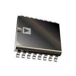
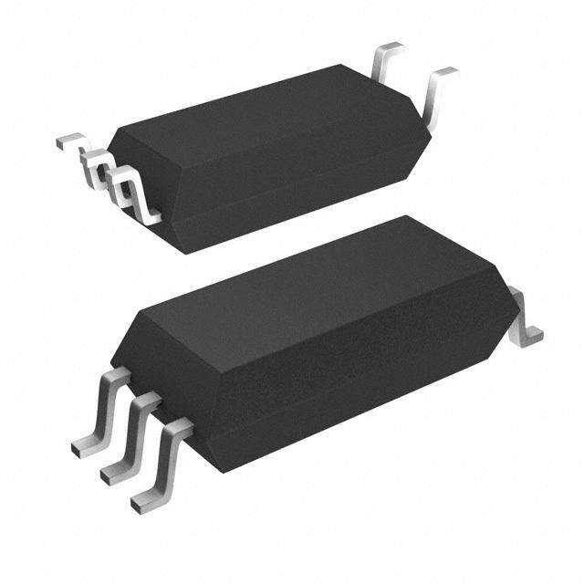
ICGOO电子元器件商城为您提供ADUM7234BRZ-RL7由Analog设计生产,在icgoo商城现货销售,并且可以通过原厂、代理商等渠道进行代购。 ADUM7234BRZ-RL7价格参考¥18.09-¥33.99。AnalogADUM7234BRZ-RL7封装/规格:隔离器 - 栅极驱动器, 4A Gate Driver Magnetic Coupling 1000Vrms 2 Channel 16-SOIC。您可以下载ADUM7234BRZ-RL7参考资料、Datasheet数据手册功能说明书,资料中有ADUM7234BRZ-RL7 详细功能的应用电路图电压和使用方法及教程。
| 参数 | 数值 |
| 产品目录 | 集成电路 (IC)半导体 |
| 描述 | IC DRIVER HALF-BRIDGE 4A 16SOIC门驱动器 Prec Half-Bridge Dvr 4A Output |
| 产品分类 | PMIC - MOSFET,电桥驱动器 - 外部开关电源管理 IC |
| 品牌 | Analog Devices |
| 产品手册 | |
| 产品图片 |
|
| rohs | 符合RoHS无铅 / 符合限制有害物质指令(RoHS)规范要求 |
| 产品系列 | 门驱动器,Analog Devices ADUM7234BRZ-RL7- |
| 数据手册 | |
| 产品型号 | ADUM7234BRZ-RL7 |
| 上升时间 | 14 ns |
| 下降时间 | 14 ns |
| 产品 | Half-Bridge Drivers |
| 产品目录页面 | |
| 产品种类 | 门驱动器 |
| 传播延迟时间 | 160 ns |
| 供应商器件封装 | 16-SOIC |
| 其它名称 | ADUM7234BRZ-RL7TR |
| 包装 | 带卷 (TR) |
| 商标 | Analog Devices |
| 安装类型 | 表面贴装 |
| 安装风格 | SMD/SMT |
| 封装 | Reel |
| 封装/外壳 | 16-SOIC(0.154",3.90mm 宽) |
| 封装/箱体 | SOIC-16 |
| 工作温度 | -40°C ~ 105°C |
| 工厂包装数量 | 1000 |
| 延迟时间 | 160ns |
| 最大工作温度 | + 125 C |
| 最小工作温度 | - 40 C |
| 标准包装 | 1,000 |
| 电压-电源 | 4.5 V ~ 5.5 V |
| 电流-峰值 | 4A |
| 电源电压-最大 | 18 V |
| 电源电压-最小 | 4.5 V |
| 电源电流 | 1.4 mA |
| 类型 | Isolated Drivers |
| 系列 | ADUM7234 |
| 视频文件 | http://www.digikey.cn/classic/video.aspx?PlayerID=1364138032001&width=640&height=505&videoID=2197917759001 |
| 输入类型 | PWM |
| 输出数 | 2 |
| 输出电压 | 12 V to 18 V |
| 输出电流 | 1.5 mA |
| 通道数量 | 2 Channel |
| 配置 | Half Bridge |
| 配置数 | 1 |
| 高压侧电压-最大值(自举) | - |


- 商务部:美国ITC正式对集成电路等产品启动337调查
- 曝三星4nm工艺存在良率问题 高通将骁龙8 Gen1或转产台积电
- 太阳诱电将投资9.5亿元在常州建新厂生产MLCC 预计2023年完工
- 英特尔发布欧洲新工厂建设计划 深化IDM 2.0 战略
- 台积电先进制程称霸业界 有大客户加持明年业绩稳了
- 达到5530亿美元!SIA预计今年全球半导体销售额将创下新高
- 英特尔拟将自动驾驶子公司Mobileye上市 估值或超500亿美元
- 三星加码芯片和SET,合并消费电子和移动部门,撤换高东真等 CEO
- 三星电子宣布重大人事变动 还合并消费电子和移动部门
- 海关总署:前11个月进口集成电路产品价值2.52万亿元 增长14.8%
PDF Datasheet 数据手册内容提取
Isolated, Precision Half-Bridge Driver, 4 A Output Data Sheet ADuM7234 FEATURES GENERAL DESCRIPTION Isolated high-side and low-side outputs The ADuM72341 is an isolated, half-bridge gate driver that Working voltage uses the Analog Devices, Inc., iCoupler® technology to provide High side or low side relative to input: ±350 V peak independent and isolated high-side and low-side outputs. High side/low side differential: 350 V peak Combining high speed CMOS and monolithic transformer 4 A peak output current technology, this isolation component provides outstanding High frequency operation: 1 MHz maximum performance characteristics superior to optocoupler-based High common-mode transient immunity: >25 kV/µs solutions. High temperature operation: 105°C By avoiding the use of LEDs and photodiodes, this iCoupler gate Narrow body, 16-lead SOIC drive device is able to provide precision timing characteristics Safety and regulatory approvals not possible with optocouplers. Furthermore, the reliability and UL recognition performance stability problems associated with optocoupler 1000 V rms for 1 minute per UL 1577 LEDs are avoided. APPLICATIONS In comparison to gate drivers that use high voltage level Isolated IGBT/MOSFET gate drives translation methodologies, the ADuM7234 offers the benefit Plasma displays of true, galvanic isolation between the input and each output Industrial inverters and between each input. Each output can be operated at up to Switching power supplies ±350 V peak relative to the input, thereby supporting low-side switching to negative voltages. The differential voltage between the high side and low side can be as high as 350 V peak. As a result, the ADuM7234 provides reliable control over the switching characteristics of IGBT/MOSFET configurations over a wide range of positive or negative switching voltages. FUNCTIONAL BLOCK DIAGRAM NC 1 ADuM7234 16 VDDA VIA 2 ENCODE DECODE 15 VOA VIB 3 14 GNDA VDD1 4 13 NC GND1 5 12 NC DISABLE 6 11 VDDB VDD1 7 ENCODE DECODE 10 VOB NC 8 9 GNDB 07990-001 Figure 1. 1 Protected by U.S. Patents 5,952,849 and 6,291,907. Rev. B Document Feedback Information furnished by Analog Devices is believed to be accurate and reliable. However, no responsibility is assumed by Analog Devices for its use, nor for any infringements of patents or other One Technology Way, P.O. Box 9106, Norwood, MA 02062-9106, U.S.A. rights of third parties that may result from its use. Specifications subject to change without notice. No license is granted by implication or otherwise under any patent or patent rights of Analog Devices. Tel: 781.329.4700 ©2010–2013 Analog Devices, Inc. All rights reserved. Trademarks and registered trademarks are the property of their respective owners. Technical Support www.analog.com
ADuM7234 Data Sheet TABLE OF CONTENTS Features .............................................................................................. 1 Regulatory Information ................................................................4 Applications ....................................................................................... 1 Absolute Maximum Ratings ............................................................5 General Description ......................................................................... 1 ESD Caution...................................................................................5 Functional Block Diagram .............................................................. 1 Pin Configuration and Function Descriptions ..............................6 Revision History ............................................................................... 2 Typical Performance Characteristics ..............................................7 Specifications ..................................................................................... 3 Applications Information .................................................................8 Electrical Characteristics ............................................................. 3 Common-Mode Transient Immunity ........................................8 Package Characteristics ............................................................... 4 Insulation Lifetime ........................................................................9 Insulation and Safety-Related Specifications ............................ 4 Outline Dimensions ....................................................................... 10 Recommended Operating Conditions ...................................... 4 Ordering Guide .......................................................................... 10 REVISION HISTORY 2/13—Rev. A to Rev. B Created Hyperlink for Safety and Regulatory Approvals Entry in Features Section ................................................................. 1 Change to Table 5 ............................................................................. 4 1/10—Revision A: Initial Version Rev. B | Page 2 of 12
Data Sheet ADuM7234 SPECIFICATIONS ELECTRICAL CHARACTERISTICS All voltages are relative to their respective grounds. 4.5 V ≤ V ≤ 5.5 V, 12 V ≤ V ≤ 18 V, and 12 V ≤ V ≤ 18 V. All minimum/ DD1 DDA DDB maximum specifications apply over the entire recommended operating range, unless otherwise noted. All typical specifications are at T = 25°C, V = 5 V, V = 15 V, and V = 15 V. A DD1 DDA DDB Table 1. Test Conditions/ Parameter Symbol Min Typ Max Unit Comments DC SPECIFICATIONS Input Supply Current, Quiescent I 1.0 2.2 mA DDI(Q) Output Supply Current A or Output Supply I , I 1.5 3.2 mA DDA(Q) DDB(Q) Current B, Quiescent Input Supply Current, 2 Mbps I 1.4 3.0 mA DDI(2) Output Supply Current A or Output Supply I , I 22 30 mA C = 1000 pF DDA(2) DDB(2) L Current B, 2 Mbps Input Currents I , I , I −10 +0.01 +10 μA 0 V ≤ V , V , V ≤ V IA IB DISABLE IA IB DISABLE DD1 Logic High Input Threshold V 0.7 × V V IH DD1 Logic Low Input Threshold V 0.3 × V V IL DD1 Logic High Output Voltages V , V V − 0.15, V , V V I , I = −20 mA OAH OBH DDA DDA DDB OA OB V − 0.15 DDB Logic Low Output Voltages V , V 0.15 V I , I = 20 mA OAL OBL OA OB Undervoltage Lockout, V or V Supply UVLO DDA DDB Positive-Going Threshold V 8.0 8.9 9.8 V DDBUV+ Negative-Going Threshold V 7.4 8.2 9.0 V DDBUV− Hysteresis V 0.3 0.7 V DDBUVH Output Short-Circuit Pulsed Current1 I , I 2.0 4.0 A OA(SC) OB(SC) SWITCHING SPECIFICATIONS C = 1000 pF L Minimum Pulse Width2 PW 100 ns Maximum Switching Frequency3 2 Mbps Propagation Delay4 t , t 130 160 200 ns PHL PLH Change vs. Temperature 130 ps/°C Pulse Width Distortion, |t − t | PWD 14 ns PLH PHL Channel-to-Channel Matching, 11 ns Rising or Falling Edges5 Channel-to-Channel Matching, 25 ns Rising vs. Falling Edges6 Part-to-Part Matching, Rising or Falling 55 ns Input t = 3 ns R Edges7 Part-to-Part Matching, Rising vs. Falling 63 ns Input t = 3 ns R Edges8 Output Rise/Fall Time (10% to 90%) t/t 8 14 30 ns R F 1 Short-circuit duration less than 1 sec. Average power must conform to the limit shown in the Absolute Maximum Ratings section. 2 The minimum pulse width is the shortest pulse width at which the specified timing parameters are guaranteed. 3 The maximum switching frequency is the maximum signal frequency at which the specified timing parameters are guaranteed. 4 tPHL propagation delay is measured from the 50% level of the falling edge of the VIx signal to the 50% level of the falling edge of the VOx signal. tPLH propagation delay is measured from the 50% level of the rising edge of the VIx signal to the 50% level of the rising edge of the VOx signal. 5 Channel-to-channel matching, rising or falling edges, is the magnitude of the propagation delay difference between two channels of the same part when the inputs are either both rising or falling edges. The supply voltages and the loads on each channel are equal. 6 Channel-to-channel matching, rising vs. falling edges, is the magnitude of the propagation delay difference between two channels of the same part when one input is a rising edge and the other input is a falling edge. The supply voltages and loads on each channel are equal. 7 Part-to-part matching, rising or falling edges, is the magnitude of the propagation delay difference between the same channels of two different parts when the inputs are either both rising or falling edges. The supply voltages, temperatures, and loads of each part are equal. 8 Part-to-part matching, rising vs. falling edges, is the magnitude of the propagation delay difference between the same channels of two different parts when one input is a rising edge and the other input is a falling edge. The supply voltages, temperatures, and loads of each part are equal. Rev. B | Page 3 of 12
ADuM7234 Data Sheet PACKAGE CHARACTERISTICS Table 2. Parameter Symbol Min Typ Max Unit Test Conditions/Comments Resistance (Input-to-Output)1 R 1012 Ω I-O Capacitance (Input-to-Output)1 C 2.0 pF f = 1 MHz I-O Input Capacitance C 4.0 pF I IC Junction-to-Ambient Thermal Resistance θ 76 °C/W JA 1 The device is considered a 2-terminal device: Pin 1 through Pin 8 are shorted together, and Pin 9 through Pin 16 are shorted together. INSULATION AND SAFETY-RELATED SPECIFICATIONS Table 3. Parameter Symbol Value Unit Test Conditions/Comments Rated Dielectric Insulation Voltage 1000 V rms 1 minute duration Minimum External Air Gap (Clearance) L(I01) 4.0 min mm Measured from input terminals to output terminals, shortest distance through air Minimum External Tracking (Creepage) L(I02) 4.0 min mm Measured from input terminals to output terminals, shortest distance path along body Minimum Internal Gap (Internal Clearance) 0.025 min mm Insulation distance through insulation Tracking Resistance (Comparative Tracking Index) CTI >600 V DIN IEC 112/VDE 0303, Part 1 Isolation Group I Material Group (DIN VDE 0110, 1/89, Table 1) Maximum Working Voltage Compatible with V 354 V peak Continuous peak voltage across the isolation barrier IORM 50 Years Service Life RECOMMENDED OPERATING CONDITIONS Table 4. Parameter Symbol Min Max Unit Operating Temperature T −40 +105 °C A Input Supply Voltage1 V 4.5 5.5 V DD1 Output Supply Voltages1 V , V 12 18 V DDA DDB Input Signal Rise and Fall Times 100 ns Common-Mode Transient Immunity2 Input-to-Output −35 +35 kV/μs Between Outputs −35 +35 kV/μs Transient Immunity, Supply Voltages2 −35 +35 kV/μs 1 All voltages are relative to their respective grounds. 2 See the Common-Mode Transient Immunity section for more information. REGULATORY INFORMATION The ADuM7234 is approved by the organization listed in Table 5. Table 5. UL Recognized under UL 1577 component recognition program1 Single/basic insulation, 1000 V rms isolation voltage File E214100 1 In accordance with UL 1577, each ADuM7234 is proof tested by applying an insulation test voltage of 1200 V rms for 1 sec (current leakage detection limit = 5 μA). Rev. B | Page 4 of 12
Data Sheet ADuM7234 ABSOLUTE MAXIMUM RATINGS Ambient temperature = 25°C, unless otherwise noted. Stresses above those listed under Absolute Maximum Ratings may cause permanent damage to the device. This is a stress Table 6. rating only; functional operation of the device at these or any Parameter Rating other conditions above those indicated in the operational Storage Temperature (T ) −55°C to +150°C ST section of this specification is not implied. Exposure to absolute Ambient Operating Temperature −40°C to +105°C maximum rating conditions for extended periods may affect (T ) A device reliability. Input Supply Voltage (V )1 −0.5 V to +7.0 V DD1 Output Supply Voltage1 −0.5 V to +27 V (V , V ) ESD CAUTION DDA DDB Input Voltage1 (V , V ) −0.5 V to V + 0.5 V IA IB DD1 Output Voltage1 V −0.5 V to V + 0.5 V OA DDA V −0.5 V to V + 0.5 V OB DDB Input-to-Output Voltage2 −350 V peak to +350 V peak Output Differential Voltage3 350 V peak Output DC Current (I , I ) −800 mA to +800 mA OA OB Common-Mode Transients4 −100 kV/µs to +100 kV/µs 1 All voltages are relative to their respective grounds. 2 Input-to-output voltage is defined as GNDA − GND1 or GNDB − GND1. 3 Output differential voltage is defined as GNDA − GNDB. 4 Refers to common-mode transients across any insulation barrier. Common- mode transients exceeding the absolute maximum ratings may cause latch-up or permanent damage. Rev. B | Page 5 of 12
ADuM7234 Data Sheet PIN CONFIGURATION AND FUNCTION DESCRIPTIONS NC 1 16 VDDA VIA 2 15 VOA VIB 3 ADuM7234 14 GNDA VDD1 4 TOP VIEW 13 NC GND1 5 (Not to Scale) 12 NC DISABLE 6 11 VDDB VDD1 7 10 VOB NC 8NC = NO CONNECT9 GNDB 07990-002 Figure 2. Pin Configuration Table 7. Pin Function Descriptions Pin No. Mnemonic Description 1, 8, 12, 13 NC No Connect. Pin 12 and Pin 13 are floating and should be left unconnected. 2 V Logic Input A. IA 3 V Logic Input B. IB 4, 7 V Input Supply Voltage, 4.5 V to 5.5 V. Pin 4 and Pin 7 are internally connected. Connecting both pins to V DD1 DD1 is recommended. 5 GND Ground Reference for Input Logic Signals. 1 6 DISABLE Input Disable. Disables the isolator inputs and refresh circuits. Outputs take on the default low state. 9 GND Ground Reference for Output B. B 10 V Output B. OB 11 V Output B Supply Voltage, 12 V to 18 V. DDB 14 GND Ground Reference for Output A. A 15 V Output A. OA 16 V Output A Supply Voltage, 12 V to 18 V. DDA Table 8. Truth Table (Positive Logic) V /V Input V State DISABLE V /V Output Notes IA IB DD1 OA OB High Powered Low High Low Powered Low Low X1 Unpowered X1 Low Output returns to the input state within 1 µs of V power restoration DD1 X1 Powered High Low 1 X is don’t care. Rev. B | Page 6 of 12
Data Sheet ADuM7234 TYPICAL PERFORMANCE CHARACTERISTICS 1.2 166 1.0 164 CHANNEL AFALL s) CHANNEL BFALL RRENT (mA)00..86 ON DELAY (n116620 CU ATI158 T G PU0.4 PA CHANNEL A RISE IN RO156 P CHANNEL B RISE 0.2 154 00 0.5 DATA RA1T.0E (Mbps) 1.5 2.0 07990-012 1524.5 INPUT SUPPL5Y.0 VOLTAGE (V) 5.5 07990-015 Figure 3. Typical Input Supply Current Variation with Data Rate Figure 6. Typical Propagation Delay Variation with Input Supply Voltage (Output Supply Voltage = 15.0 V) 25 166 164 CHANNEL AFALL mA) 20 Y (ns)162 CHANNEL BFALL RRENT ( 15 N DELA160 U O PUT C 10 AGATI158 CHANNEL A RISE T P OU RO156 P 5 CHANNEL B RISE 154 00 0.5 DATA RA1T.0E (Mbps) 1.5 2.0 07990-013 15212 OUTPUT SUPP1L5Y VOLTAGE (V) 18 07990-016 Figure 4. Typical Output Supply Current Variation with Data Rate Figure 7. Typical Propagation Delay Variation with Output Supply Voltage (Input Supply Voltage = 5.0 V) 160 s)155 n Y ( A L E D ON 150 TI A G A P O PR145 140–40 –20 0 T2E0MPERA4T0URE (6°0C) 80 100 120 07990-014 Figure 5. Typical Propagation Delay Variation with Temperature Rev. B | Page 7 of 12
ADuM7234 Data Sheet APPLICATIONS INFORMATION COMMON-MODE TRANSIENT IMMUNITY Figure 9 and Figure 10 characterize the ability of the ADuM7234 to operate correctly in the presence of sinusoidal In general, common-mode transients consist of linear and transients. The data is based on design simulation and is the sinusoidal components. The linear component of a common- maximum sinusoidal transient magnitude (2πf V) that the mode transient is given by 0 ADuM7234 can tolerate without an operational error. Values V = (ΔV/Δt)t CM, linear for immunity against sinusoidal transients are not included in where ΔV/Δt is the slope of the transient shown in Figure 11 Table 4 because measurements to obtain such values have not and Figure 12. been possible. The transient of the linear component is given by 250 dV /dt = ΔV/Δt CM 200 Figure 8 characterizes the ability of the ADuM7234 to operate s) µ correctly in the presence of linear transients. The data, based on kV/ design simulation, is the maximum linear transient magnitude TY (150 that the ADuM7234 can tolerate without an operational error. MUNI BWEOSRTS-CTA-CSAES PER PORCOECSESSVSAVRAIARTIAIOTINON M This data shows a correlation with the data that is listed in T I100 N Table 4, which is based on measured data. E SI N 50 TRA 50 45 40 TY (kV/µs)3350 00Figur2e5 09. Tra5n0s0ient 7FIm5R0EmQuUn1E0iNt0yC0 (YS (iMn1uH25szo0)ida1l 5T0r0ansi1e7n5t0s), 2000 07990-004 NI MU25 27°C Ambient Temperature M T I20 250 N SIE15 BEST-CASE PROCESSVARIATION N WORST-CASE PROCESSVARIATION A TR10 µs)200 V/ 5 Y (k Fig0u–4re0 8. Tra–2n0sient Im0muTnEiMty2P 0(ELRinAeTaUrR4 TE0r a(°nCs)ien60ts) vs. T8e0mpera1t0u0re07990-003 NT IMMUNIT110500 BWEOSRTS-CTA-CSAES PER PORCOECSESSVSAVRAIARTIAIOTINON E SI The sinusoidal component (at a given frequency) is given by AN R T 50 V = Vsin(2πft) CM, sinusoidal 0 where: Vf i0s itsh teh fer emqaugennictuy doef othf et hsein suinsouisdoaidl. al. 00 250 500 7F5R0EQU1E0N0C0Y (M1H25z0) 1500 1750 2000 07990-005 Figure 10. Transient Immunity (Sinusoidal Transients), The transient magnitude of the sinusoidal component is given by 100°C Ambient Temperature dV /dt = 2πf V CM 0 Rev. B | Page 8 of 12
Data Sheet ADuM7234 15V VDD1 5V The insulation lifetime of the ADuM7234 depends on the GND1 voltage waveform type imposed across the isolation barrier. VDDAANDVDDB 15V The iCoupler insulation structure degrades at different rates GNDAAND GNDB GVNDDDAAAANNDD GVNDDDBB 15V5V ΔΔVt ΔV 15V dace,p oern ddcin. gF iognu rwe h1e4t,h Feirg uthree w15a,v aenfodr mFi gius rbei p1o6l ailrl uasct,r uatnei pthoelasre GVNDDD11 Δt 07990-006 dBiifpfoerlaern ta cis voolalttaiogne ivso tlhtaeg me wosatv setfroirnmgesn. t environment. The goal Figure 11. Common-Mode Transient Immunity Waveforms, Input to Output of a 50-year operating lifetime under the bipolar ac condition determines the maximum working voltage recommended by 15V VDDA/VDDB 15V Analog Devices. GNDA/GNDB VDDB/VDDA 15V In the case of unipolar ac or dc voltage, the stress on the insulation GNDB/GNDA is significantly lower. This allows operation at higher working VDDA/VDDB 15V ΔΔVt voltages while still achieving a 50-year service life. The working GNDA/GNDB 15V ΔV 15V GVNDDDAB/G/VNDDDBA Δt 07990-007 v5o0l-tyaegaer lmistiendim inu mTa blilfee t3im caen, pbreo avpidpelide dth wath tihlee mvoalitnatgaei ncionngf othrme s Figure 12. Common-Mode Transient Immunity Waveforms to either the unipolar ac or dc voltage cases. Any cross-insulation Between Outputs voltage waveform that does not conform to Figure 15 or Figure 16 should be treated as a bipolar ac waveform, and its peak voltage VDDA/VDDB should be limited to the 50-year lifetime voltage value listed in Table 3. VGDNDDAA/V/GDNDBDB ΔVΔDtD GNDA/GNDB 07990-008 Nsooidtea lt hfoart tilhlue svtoralttaiogne ppruerspeonsteesd oinn lFy.i gItu irse m15e aisn ts htoo wrenp aress seinntu a-ny Figure 13. Transient Immunity Waveforms, Output Supplies voltage waveform varying between 0 V and some limiting value. INSULATION LIFETIME The limiting value can be positive or negative, but the voltage cannot cross 0 V. All insulation structures eventually break down when subjected to voltage stress over a sufficiently long period. The rate of insu- lation degradation depends on the characteristics of the voltage RATED PEAK VOLTAGE wpearvfeofromrmed a bpyp ltihede arecgrouslsa ttohrey i nagsuenlactiieosn, .A Inn aaldodgi tDioenv itcoe tsh ceo tnedstuincgts 0V 07990-009 an extensive set of evaluations to determine the lifetime of the Figure 14. Bipolar AC Waveform insulation structure within the ADuM7234. Analog Devices performs accelerated life testing using voltage RATED PEAK VOLTAGE levels higher than the rated continuous working voltage. Accel- eTrhaetisoen fa fcatcotrosr as lfloorw s ceavlecrualla otipoenr oatfi tnhge ctoimnde ittoio fnasil uarree adte ttherem acintueadl. 0V 07990-010 Figure 15. Unipolar AC Waveform working voltage. Table 3 lists the peak voltage for 50 years of service life for a bipolar ac operating condition and the maximum Analog Devices recommended working voltage. In many cases, RATED PEAK VOLTAGE the approved working voltage is higher than the 50-year service ltiofe s hvoolrttaegnee. dO ipnesuralatitoionn a lti fteh einse s hoimghe cwaosreks.i ng voltages can lead 0V 07990-011 Figure 16. DC Waveform Rev. B | Page 9 of 12
ADuM7234 Data Sheet OUTLINE DIMENSIONS 10.00 (0.3937) 9.80 (0.3858) 4.00 (0.1575) 16 9 6.20 (0.2441) 3.80 (0.1496) 1 8 5.80 (0.2283) 1.27 (0.0500) 0.50 (0.0197) BSC 1.75 (0.0689) 0.25 (0.0098) 45° 0.25 (0.0098) 1.35 (0.0531) 8° 0.10 (0.0039) 0° COPL0A.1N0ARITY 0.51 (0.0201) SPELAATNIENG 0.25 (0.0098) 1.27 (0.0500) 0.31 (0.0122) 0.17 (0.0067) 0.40 (0.0157) COMPLIANTTO JEDEC STANDARDS MS-012-AC C(RINOEFNPEATRRREOENNLCLTEIHN EOGSN EDLSIYM)AEANNRDSEI AORRNOESU NANORDEET DAIN-PO MPFRIFLO LMPIIMRLELIATIMTEEER TFSEO; RIRN ECUQHSU EDI VIINMA LEDENENSSTIIOGSN NFS.OR 060606-A Figure 17. 16-Lead Standard Small Outline Package [SOIC_N] Narrow Body (R-16) Dimensions shown in millimeters and (inches) ORDERING GUIDE Number of Output Peak Output Package Model1 Channels Current (A) Voltage (V) Temperature Range Package Description Option ADuM7234BRZ 2 4 15 −40°C to +105°C 16-Lead SOIC_N R-16 ADuM7234BRZ-RL7 2 4 15 −40°C to +105°C 16-Lead SOIC_N, 7-Inch Tape R-16 and Reel Option (1,000 Units) 1 Z = RoHS Compliant Part. Rev. B | Page 10 of 12
Data Sheet ADuM7234 NOTES Rev. B | Page 11 of 12
ADuM7234 Data Sheet NOTES ©2010–2013 Analog Devices, Inc. All rights reserved. Trademarks and registered trademarks are the property of their respective owners. D07990-0-2/13(B) Rev. B | Page 12 of 12
Mouser Electronics Authorized Distributor Click to View Pricing, Inventory, Delivery & Lifecycle Information: A nalog Devices Inc.: ADUM7234BRZ-RL7 ADUM7234BRZ