 Datasheet下载
- 型号: ADUM2285BRIZ
- 制造商: Analog
- 库位|库存: xxxx|xxxx
- 要求:
| 数量阶梯 | 香港交货 | 国内含税 |
| +xxxx | $xxxx | ¥xxxx |
查看当月历史价格
查看今年历史价格
ADUM2285BRIZ产品简介:
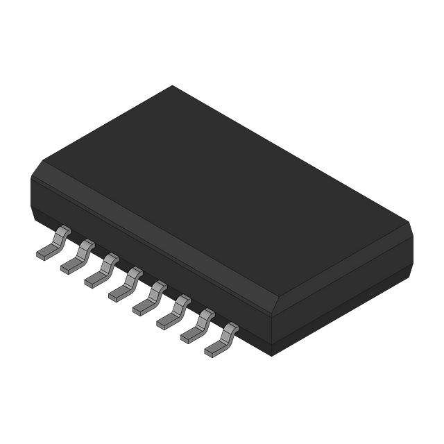
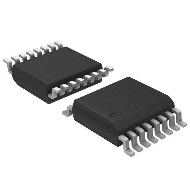
ICGOO电子元器件商城为您提供ADUM2285BRIZ由Analog设计生产,在icgoo商城现货销售,并且可以通过原厂、代理商等渠道进行代购。 ADUM2285BRIZ价格参考。AnalogADUM2285BRIZ封装/规格:数字隔离器, General Purpose Digital Isolator 5000Vrms 2 Channel 25Mbps 25kV/µs CMTI 16-SOIC (0.295", 7.50mm Width)。您可以下载ADUM2285BRIZ参考资料、Datasheet数据手册功能说明书,资料中有ADUM2285BRIZ 详细功能的应用电路图电压和使用方法及教程。
| 参数 | 数值 |
| 产品目录 | |
| ChannelType | 单向 |
| 描述 | IC DGTL ISO 2CH LOGIC 16SOIC数字隔离器 5kV RMS Dual CH Digital |
| 产品分类 | |
| IsolatedPower | 无 |
| 品牌 | Analog Devices |
| 产品手册 | |
| 产品图片 |
|
| rohs | 符合RoHS无铅 / 符合限制有害物质指令(RoHS)规范要求 |
| 产品系列 | 接口 IC,数字隔离器,Analog Devices ADUM2285BRIZiCoupler® |
| 数据手册 | |
| 产品型号 | ADUM2285BRIZ |
| PCN设计/规格 | |
| PulseWidthDistortion(Max) | 3ns |
| 上升/下降时间(典型值) | 2.5ns, 2.5ns |
| 产品种类 | |
| 传播延迟tpLH/tpHL(最大值) | 39ns, 39ns |
| 传播延迟时间 | 35 ns |
| 供应商器件封装 | 16-SOIC-IC |
| 共模瞬态抗扰度(最小值) | 25kV/µs |
| 包装 | 管件 |
| 商标 | Analog Devices |
| 安装风格 | SMD/SMT |
| 封装 | Tube |
| 封装/外壳 | 16-SOIC(0.295",7.50mm 宽) |
| 封装/箱体 | SOIC-16 |
| 工作温度 | -40°C ~ 125°C |
| 工厂包装数量 | 37 |
| 技术 | 磁耦合 |
| 数据速率 | 25Mbps |
| 最大工作温度 | + 125 C |
| 最大数据速率 | 25 Mb/s |
| 最小工作温度 | - 40 C |
| 标准包装 | 37 |
| 电压-电源 | 2.7 V ~ 5.5 V |
| 电压-隔离 | 5000Vrms |
| 电源电压-最大 | 5.5 V |
| 电源电流 | 0.8 mA |
| 类型 | General Purpose |
| 系列 | ADuM2285 |
| 绝缘电压 | 5 kVrms |
| 脉宽失真(最大) | 3ns |
| 视频文件 | http://www.digikey.cn/classic/video.aspx?PlayerID=1364138032001&width=640&height=505&videoID=2219593469001http://www.digikey.cn/classic/video.aspx?PlayerID=1364138032001&width=640&height=505&videoID=2219593470001http://www.digikey.cn/classic/video.aspx?PlayerID=1364138032001&width=640&height=505&videoID=2219614223001 |
| 输入-输入侧1/输入侧2 | 2/0 |
| 通道数 | 2 |
| 通道数量 | 2 Channel |
| 通道类型 | 单向 |
| 隔离式电源 | 无 |


- 商务部:美国ITC正式对集成电路等产品启动337调查
- 曝三星4nm工艺存在良率问题 高通将骁龙8 Gen1或转产台积电
- 太阳诱电将投资9.5亿元在常州建新厂生产MLCC 预计2023年完工
- 英特尔发布欧洲新工厂建设计划 深化IDM 2.0 战略
- 台积电先进制程称霸业界 有大客户加持明年业绩稳了
- 达到5530亿美元!SIA预计今年全球半导体销售额将创下新高
- 英特尔拟将自动驾驶子公司Mobileye上市 估值或超500亿美元
- 三星加码芯片和SET,合并消费电子和移动部门,撤换高东真等 CEO
- 三星电子宣布重大人事变动 还合并消费电子和移动部门
- 海关总署:前11个月进口集成电路产品价值2.52万亿元 增长14.8%


PDF Datasheet 数据手册内容提取
5 kV RMS Dual Channel Digital Isolators Data Sheet ADuM2280/ADuM2281/ADuM2285/ADuM2286 FEATURES GENERAL DESCRIPTION High isolation voltage: 5000 V rms The ADuM2280/ADuM2281/ADuM2285/ADuM22861 (also Up to 100 Mbps data rate referred to as ADuM228x in this data sheet) are 5 kV rms dual- Low propagation delay: 24 ns maximum channel digital isolators based on Analog Devices, Inc., iCoupler® Low dynamic power consumption technology. Combining high speed CMOS and monolithic air Bidirectional communication core transformer technology, these isolation components 3 V to 5 V level translation provide outstanding performance characteristics superior to High temperature operation: 125°C alternatives, such as optocoupler devices and other integrated High common-mode transient immunity: >25 kV/μs couplers. Default high output: ADuM2280/ADuM2281 With propagation delay at 24 ns maximum, pulse width Default low output: ADuM2285/ADuM2286 distortion is less than 2 ns for C grade. Channel-to-channel 16-lead SOIC wide body enhanced creepage package matching is tight at 5 ns for C grade. The ADuM228x are Safety and regulatory approvals (pending) available in two channel configurations with three different UL recognition: 5000 V rms for 1 minute per UL 1577 data rates up to 100 Mbps (see the Ordering Guide). All models CSA Component Acceptance Notice #5A operate with the supply voltage on either side ranging from IEC 60601-1: 250 V rms (reinforced) 2.7 V to 5.5 V, providing compatibility with lower voltage IEC 60950-1: 400 V rms (reinforced) systems as well as enabling a voltage translation functionality VDE Certificate of Conformity across the isolation barrier. Unlike other optocoupler DIN V VDE V 0884-10 (VDE V 0884-10): 2006-12 alternatives, the ADuM228x isolators have a patented refresh V = 846 V peak IORM feature that ensures dc correctness in the absence of input logic Pin-compatible with ADuM220x and ADuM221x families transitions. When power is first applied or is not yet applied to APPLICATIONS the input side, the ADuM2280 and ADuM2281 have a default General-purpose, high voltage, multichannel isolation high output and the ADuM2285 and ADuM2286 have a default Medical equipment low output. Power supplies RS-232/RS-422/RS-485 transceiver isolation FUNCTIONAL BLOCK DIAGRAMS GND1 1 PIN 1 ADuM2280/ 16 GND2 GND1 1 PIN 1 ADuM2281/ 16 GND2 INDICATOR INDICATOR NC 2 ADuM2285 15 NC NC 2 ADuM2286 15 NC VDD1 3 14 VDD2 VDD1 3 14 VDD2 VIA 4 ENCODE DECODE 13 VOA VOA 4 DECODE ENCODE 13 VIA VIB 5 ENCODE DECODE 12 VOB VIB 5 ENCODE DECODE 12 VOB NC 6 11 NC NC 6 11 NC GND1 7 10 NC GND1 7 10 NC NC 8NC = NO CONNECT 9 GND2 10446-001 NC 8NC = NO CONNECT 9 GND2 10446-002 Figure 1. ADuM2280/ADuM2285 Figure 2. ADuM2281/ADuM2286 Pin-Compatible with ADuM2200/ADuM2210 Pin-Compatible with ADuM2201/ADuM2211 1 Protected by U.S. Patents 5,952,849; 6,873,065; 6,903,578; and 7,075,329. Other patents are pending. Rev. A Document Feedback Information furnished by Analog Devices is believed to be accurate and reliable. However, no responsibility is assumed by Analog Devices for its use, nor for any infringements of patents or other One Technology Way, P.O. Box 9106, Norwood, MA 02062-9106, U.S.A. rights of third parties that may result from its use. Specifications subject to change without notice. No license is granted by implication or otherwise under any patent or patent rights of Analog Devices. Tel: 781.329.4700 ©2012–2019 Analog Devices, Inc. All rights reserved. Trademarks and registered trademarks are the property of their respective owners. Technical Support www.analog.com
ADuM2280/ADuM2281/ADuM2285/ADuM2286 Data Sheet TABLE OF CONTENTS Features .............................................................................................. 1 Recommended Operating Conditions .......................................8 Applications ....................................................................................... 1 Absolute Maximum Ratings ............................................................9 General Description ......................................................................... 1 ESD Caution...................................................................................9 Functional Block Diagrams ............................................................. 1 Pin Configurations and Function Descriptions ......................... 10 Revision History ............................................................................... 2 Typical Performance Characteristics ........................................... 13 Specifications ..................................................................................... 3 Applications Information .............................................................. 14 Electrical Characteristics—5 V Operation................................ 3 PC Board Layout ........................................................................ 14 Electrical Characteristics—3 V Operation................................ 4 Propagation Delay-Related Parameters ................................... 14 Electrical Characteristics—Mixed 5 V/3 V Operation............ 5 DC Correctness and Magnetic Field Immunity........................... 14 Electrical Characteristics—Mixed 3 V/5 V Operation............ 6 Power Consumption .................................................................. 15 Package Characteristics ............................................................... 7 Insulation Lifetime ..................................................................... 16 Regulatory Information ............................................................... 7 Outline Dimensions ....................................................................... 17 Insulation and Safety-Related Specifications ............................ 7 Ordering Guide .......................................................................... 17 DIN V VDE V 0884-10 (VDE V 0884-10) Insulation Characteristics .............................................................................. 8 REVISION HISTORY 5/2019—Rev. 0 to Rev. A Change to After Input and/or Safety Test Subgroup 2 and Subgroup 3 Parameter, Table 16 ..................................................... 8 Updated Outline Dimensions ....................................................... 17 11/2012—Revision 0: Initial Version Rev. A | Page 2 of 20
Data Sheet ADuM2280/ADuM2281/ADuM2285/ADuM2286 SPECIFICATIONS ELECTRICAL CHARACTERISTICS—5 V OPERATION All typical specifications are at T = 25°C, V = V = 5 V. Minimum/maximum specifications apply over the entire recommended A DD1 DD2 operation range: 4.5 V ≤ V ≤ 5.5 V, 4.5 V ≤ V ≤ 5.5 V, −40°C ≤ T ≤ 125°C, unless otherwise noted. Switching specifications are DD1 DD2 A tested with C = 15 pF and CMOS signal levels, unless otherwise noted. L Table 1. A Grade B Grade C Grade Parameter Symbol Min Typ Max Min Typ Max Min Typ Max Unit Test Conditions SWITCHING SPECIFICATIONS Pulse Width PW 1000 40 10 ns Within PWD limit Data Rate 1 25 100 Mbps Within PWD limit Propagation Delay tPHL, tPLH 50 39 13 20 24 ns 50% input to 50% output Pulse Width Distortion PWD 10 3 2 ns |tPLH − tPHL| Change vs. Temperature 7 3 1.5 ps/°C Propagation Delay Skew tPSK 38 12 9 ns Between any two units at same operating conditions Channel Matching Codirectional tPSKCD 5 3 2 ns Opposing Direction tPSKOD 10 6 5 ns Jitter 2 2 1 ns Table 2. 1 Mbps—A, B, C Grades 25 Mbps—B, C Grades 100 Mbps—C Grade Parameter Symbol Min Typ Max Min Typ Max Min Typ Max Unit Test Conditions SUPPLY CURRENT No load ADuM2280/ADuM2285 IDD1 1.3 1.6 6.2 7.0 20 25 mA IDD2 2.7 4.5 4.8 7.0 9.5 15 mA ADuM2281/ADuM2286 IDD1 2.3 2.6 5.8 6.5 16 19 mA IDD2 2.3 2.9 5.8 6.5 16.5 19 mA Table 3. For All Models Parameter Symbol Min Typ Max Unit Test Conditions DC SPECIFICATIONS Logic High Input Threshold VIH 0.7 VDDx V Logic Low Input Threshold VIL 0.3 VDDx V Logic High Output Voltages VOH VDDx − 0.1 5.0 V IOx = −20 µA, VIx = VIxH VDDx − 0.4 4.8 V IOx = −4 mA, VIx = VIxH Logic Low Output Voltages VOL 0.0 0.1 V IOx = 20 µA, VIx = VIxL 0.2 0.4 V IOx = 4 mA, VIx = VIxL Input Current per Channel II −10 +0.01 +10 µA 0 V ≤ VIx ≤ VDDx Supply Current per Channel Quiescent Input Supply Current IDDI(Q) 0.54 0.8 mA Quiescent Output Supply Current IDDO(Q) 1.6 2.0 mA Dynamic Input Supply Current IDDI(D) 0.09 mA/Mbps Dynamic Output Supply Current IDDO(D) 0.04 mA/Mbps Undervoltage Lockout Positive VDDx Threshold VDDxUV+ 2.6 V Negative VDDx Threshold VDDxUV- 2.4 V VDDx Hysteresis VDDxUVH 0.2 V AC SPECIFICATIONS Output Rise/Fall Time tR/tF 2.5 ns 10% to 90% Common-Mode Transient Immunity1 |CM| 25 35 kV/µs VIx = VDDx, VCM = 1000 V, transient magnitude = 800 V Refresh Period tr 1.6 µs 1 |CM| is the maximum common-mode voltage slew rate that can be sustained while maintaining VO > 0.8 VDDx. The common-mode voltage slew rates apply to both rising and falling common-mode voltage edges. Rev. A | Page 3 of 20
ADuM2280/ADuM2281/ADuM2285/ADuM2286 Data Sheet ELECTRICAL CHARACTERISTICS—3 V OPERATION All typical specifications are at T = 25°C, V = V = 3.0 V. Minimum/maximum specifications apply over the entire recommended A DD1 DD2 operation range: 2.7 V ≤ V ≤ 3.6 V, 2.7 V ≤ V ≤ 3.6 V, −40°C ≤ T ≤ 125°C, unless otherwise noted. Switching specifications are DD1 DD2 A tested with C = 15 pF and CMOS signal levels, unless otherwise noted. L Table 4. A Grade B Grade C Grade Parameter Symbol Min Typ Max Min Typ Max Min Typ Max Unit Test Conditions SWITCHING SPECIFICATIONS Pulse Width PW 1000 40 10 ns Within PWD limit Data Rate 1 25 100 Mbps Within PWD limit Propagation Delay tPHL, tPLH 50 39 20 28 35 ns 50% input to 50% output Pulse Width Distortion PWD 10 3 2.5 ns |tPLH − tPHL| Change vs. Temperature 7 3 1.5 ps/°C Propagation Delay Skew tPSK 38 16 12 ns Between any two units at same operating conditions Channel Matching Codirectional tPSKCD 5 3 2.5 ns Opposing-Direction tPSKOD 10 6 5 ns Jitter 2 2 1 ns Table 5. 1 Mbps—A, B, C Grades 25 Mbps—B, C Grades 100 Mbps—C Grade Parameter Symbol Min Typ Max Min Typ Max Min Typ Max Unit Test Conditions SUPPLY CURRENT No load ADuM2280/ADuM2285 IDD1 0.75 1.4 5.1 9.0 17 23 mA IDD2 2.0 3.5 2.7 4.6 4.8 9 mA ADuM2281/ADuM2286 IDD1 1.6 2.1 3.8 5.0 11 15 mA IDD2 1.7 2.3 3.9 6.2 11 15 mA Table 6. For All Models Parameter Symbol Min Typ Max Unit Test Conditions DC SPECIFICATIONS Logic High Input Threshold VIH 0.7 VDDx V Logic Low Input Threshold VIL 0.3 VDDx V Logic High Output Voltages VOH VDDx − 0.1 3.0 V IOx = −20 µA, VIx = VIxH VDDx − 0.4 2.8 V IOx = −4 mA, VIx = VIxH Logic Low Output Voltages VOL 0.0 0.1 V IOx = 20 µA, VIx = VIxL 0.2 0.4 V IOx = 4 mA, VIx = VIxL Input Current per Channel II −10 +0.01 +10 µA 0 V ≤ VIx ≤ VDDx Supply Current per Channel Quiescent Input Supply Current IDDI(Q) 0.4 0.6 mA Quiescent Output Supply Current IDDO(Q) 1.2 1.7 mA Dynamic Input Supply Current IDDI(D) 0.08 mA/Mbps Dynamic Output Supply Current IDDO(D) 0.015 mA/Mbps Undervoltage Lockout Positive VDDx Threshold VDDxUV+ 2.6 V Negative VDDx Threshold VDDxUV− 2.4 V VDDx Hysteresis VDDxUVH 0.2 V AC SPECIFICATIONS Output Rise/Fall Time tR/tF 3 ns 10% to 90% Common-Mode Transient Immunity1 |CM| 25 35 kV/µs VIx = VDDx, VCM = 1000 V, transient magnitude = 800 V Refresh Period tr 1.6 µs 1 |CM| is the maximum common-mode voltage slew rate that can be sustained while maintaining VO > 0.8 VDDx. The common-mode voltage slew rates apply to both rising and falling common-mode voltage edges. Rev. A | Page 4 of 20
Data Sheet ADuM2280/ADuM2281/ADuM2285/ADuM2286 ELECTRICAL CHARACTERISTICS—MIXED 5 V/3 V OPERATION All typical specifications are at T = 25°C, V = 5 V, V = 3.0 V. Minimum/maximum specifications apply over the entire recom- A DD1 DD2 mended operation range: 4.5 V ≤ V ≤ 5.5 V, 2.7 V ≤ V ≤ 3.6 V; and −40°C ≤ T ≤ 125°C, unless otherwise noted. Switching DD1 DD2 A specifications are tested with C = 15 pF and CMOS signal levels, unless otherwise noted. L Table 7. A Grade B Grade C Grade Parameter Symbol Min Typ Max Min Typ Max Min Typ Max Unit Test Conditions SWITCHING SPECIFICATIONS Pulse Width PW 1000 40 10 ns Within PWD limit Data Rate 1 25 100 Mbps Within PWD limit Propagation Delay tPHL, tPLH 50 39 13 20 26 ns 50% input to 50% output Pulse Width Distortion PWD 10 3 2 ns |tPLH − tPHL| Change vs. Temperature 7 3 1.5 ps/°C Propagation Delay Skew tPSK 38 16 12 ns Between any two units at same operating conditions Channel Matching Codirectional tPSKCD 5 3 2 ns Opposing-Direction tPSKOD 10 6 5 ns Jitter 2 2 1 ns Table 8. 1 Mbps—A, B, C Grades 25 Mbps—B, C Grades 100 Mbps—C Grades Parameter Symbol Min Typ Max Min Typ Max Min Typ Max Unit Test Conditions SUPPLY CURRENT No load ADuM2280/ADuM2285 IDD1 1.3 1.6 6.2 7.0 20 25 mA IDD2 2.0 3.5 2.7 4.6 4.8 9.0 mA ADuM2281/ADuM2286 IDD1 2.3 2.6 5.8 6.5 16 19 mA IDD2 1.7 2.3 3.9 6.2 11 15 mA Table 9. For All Models Parameter Symbol Min Typ Max Unit Test Conditions DC SPECIFICATIONS Logic High Input Threshold VIH 0.7 VDDx V Logic Low Input Threshold VIL 0.3 VDDx V Logic High Output Voltages VOH VDDx − 0.1 VDDx V IOx = −20 µA, VIx = VIxH VDDx − 0.4 VDDx − 0.2 V IOx = −4 mA, VIx = VIxH Logic Low Output Voltages VOL 0.0 0.1 V IOx = 20 µA, VIx = VIxL 0.2 0.4 V IOx = 4 mA, VIx = VIxL Input Current per Channel II −10 +0.01 +10 µA 0 V ≤ VIx ≤ VDDx Supply Current per Channel Quiescent Input Supply Current IDDI(Q) 0.54 0.75 mA Quiescent Output Supply Current IDDO(Q) 1.2 2.0 mA Dynamic Input Supply Current IDDI(D) 0.09 mA/Mbps Dynamic Output Supply Current IDDO(D) 0.02 mA/Mbps Undervoltage Lockout Positive VDDx Threshold VDDxUV+ 2.6 V Negative VDDx Threshold VDDxUV− 2.4 V VDDx Hysteresis VDDxUVH 0.2 V AC SPECIFICATIONS Output Rise/Fall Time tR/tF 2.5 ns 10% to 90% Common-Mode Transient Immunity1 |CM| 25 35 kV/µs VIx = VDDx, VCM = 1000 V, transient magnitude = 800 V Refresh Period tr 1.6 µs 1 |CM| is the maximum common-mode voltage slew rate that can be sustained while maintaining VO > 0.8 VDDx. The common-mode voltage slew rates apply to both rising and falling common-mode voltage edges. Rev. A | Page 5 of 20
ADuM2280/ADuM2281/ADuM2285/ADuM2286 Data Sheet ELECTRICAL CHARACTERISTICS—MIXED 3 V/5 V OPERATION All typical specifications are at T = 25°C, V = 3.0 V, V = 5 V. Minimum/maximum specifications apply over the entire recom- A DD1 DD2 mended operation range: 2.7 V ≤ V ≤ 3.6 V, 4.5 V ≤ V ≤ 5.5 V; and −40°C ≤ T ≤ 125°C, unless otherwise noted. Switching DD1 DD2 A specifications are tested with C = 15 pF and CMOS signal levels, unless otherwise noted. L Table 10. A Grade B Grade C Grade Parameter Symbol Min Typ Max Min Typ Max Min Typ Max Unit Test Conditions SWITCHING SPECIFICATIONS Pulse Width PW 1000 40 10 ns Within PWD limit Data Rate 1 25 100 Mbps Within PWD limit Propagation Delay tPHL, tPLH 50 39 16 24 30 ns 50% input to 50% output Pulse Width Distortion PWD 10 3 2.5 ns |tPLH − tPHL| Change vs. Temperature 7 3 1.5 ps/C Propagation Delay Skew tPSK 38 16 12 ns Between any two units at same operating conditions Channel Matching Codirectional tPSKCD 5 3 2.5 ns Opposing-Direction tPSKOD 10 6 5 ns Jitter 2 2 1 ns Table 11. 1 Mbps—A, B, C Grades 25 Mbps—B, C Grades 100 Mbps—C Grade Parameter Symbol Min Typ Max Min Typ Max Min Typ Max Unit Test Conditions SUPPLY CURRENT No load ADuM2280/ADuM2285 IDD1 0.75 1.4 5.1 9.0 17 23 mA IDD2 2.7 4.5 4.8 7.0 9.5 15 mA ADuM2281/ADuM2286 IDD1 1.6 2.1 3.8 5.0 11 15 mA IDD2 1.7 2.3 5.8 6.5 16.5 19 mA Table 12. For All Models Parameter Symbol Min Typ Max Unit Test Conditions DC SPECIFICATIONS Logic High Input Threshold VIH 0.7 VDDx V Logic Low Input Threshold VIL 0.3 VDDx V Logic High Output Voltages VOH VDDx − 0.1 VDDx V IOx = −20 µA, VIx = VIxH VDDx − 0.4 VDDx − 0.2 V IOx = −4 mA, VIx = VIxH Logic Low Output Voltages VOL 0.0 0.1 V IOx = 20 µA, VIx = VIxL 0.2 0.4 V IOx = 4 mA, VIx = VIxL Input Current per Channel II −10 +0.01 +10 µA 0 V ≤ VIx ≤ VDDx Supply Current per Channel Quiescent Input Supply Current IDDI(Q) 0.4 0.75 mA Quiescent Output Supply Current IDDO(Q) 1.6 2.0 mA Dynamic Input Supply Current IDDI(D) 0.08 mA/Mbps Dynamic Output Supply Current IDDO(D) 0.03 mA/Mbps Undervoltage Lockout Positive VDDx Threshold VDDxUV+ 2.6 V Negative VDDx Threshold VDDxUV− 2.4 V VDDx Hysteresis VDDxUVH 0.2 V AC SPECIFICATIONS Output Rise/Fall Time tR/tF 2.5 ns 10% to 90% Common-Mode Transient Immunity1 |CM| 25 35 kV/µs VIx = VDDx, VCM = 1000 V, transient magnitude = 800 V Refresh Period tr 1.6 µs 1 |CM| is the maximum common-mode voltage slew rate that can be sustained while maintaining VO > 0.8 VDDx. The common-mode voltage slew rates apply to both rising and falling common-mode voltage edges. Rev. A | Page 6 of 20
Data Sheet ADuM2280/ADuM2281/ADuM2285/ADuM2286 PACKAGE CHARACTERISTICS Table 13. Parameter Symbol Min Typ Max Unit Test Conditions RESISTANCE AND CAPACITANCE Resistance (Input-to-Output)1 R 1013 Ω I-O Capacitance (Input-to-Output)1 C 2.2 pF f = 1 MHz I-O Input Capacitance2 C 4.0 pF I IC Junction to Ambient Thermal θ 45 °C/W Thermocouple located at the center of the package JA Resistance underside; test conducted on a 4-layer board with thin traces 1 This device is considered a 2-terminal device; Pin 1 through Pin 8 are shorted together and Pin 9 through Pin 16 are shorted together. 2 Input capacitance is from any input data pin to ground. REGULATORY INFORMATION The ADuM228x will be approved by the organizations listed in Table 14. See Table 19 and the Absolute Maximum Ratings section for recommended maximum working voltages for specific cross-isolation waveforms and insulation levels. Table 14. UL (Pending) CSA (Pending) VDE (Pending) Recognized under UL 1577 Approved under CSA Component Certified according to DIN V VDE V 0884-10 Component Recognition Acceptance Notice #5A (VDE V 0884-10): 2006-122 Program1 Single Protection 5000 V rms Basic insulation per CSA 60950-1-07 and Reinforced insulation, 846 V peak Isolation Voltage IEC 60950-1, 600 V rms (848 V peak) maximum working voltage Reinforced insulation per CSA 60950-1-07 and IEC 60950-1, 400 V rms (565 V peak) maximum working voltage Reinforced insulation per IEC 60601-1 250 V rms (353 V peak) maximum working voltage File E214100 File 205078 File 2471900-4880-0001 1 In accordance with UL 1577, each ADuM228x is proof tested by applying an insulation test voltage ≥ 6000 V rms for 1 second (current leakage detection limit = 10 μA). 2 In accordance with DIN V VDE V 0884-10, each ADuM228x is proof tested by applying an insulation test voltage ≥1590 V peak for 1 sec (partial discharge detection limit = 5 pC). The * marking branded on the component designates DIN V VDE V 0884-10 approval. INSULATION AND SAFETY-RELATED SPECIFICATIONS Table 15. Parameter Symbol Value Unit Test Conditions Rated Dielectric Insulation Voltage 5000 V rms 1-minute duration Minimum External Air Gap L(I01) 8.0 min mm Distance measured from input terminals to output terminals, shortest distance through air along the PCB mounting plane, as an aid to PC board layout Minimum External Tracking (Creepage) L(I02) 8.3 min mm Measured from input terminals to output terminals, shortest distance path along body Minimum Internal Gap (Internal Clearance) 0.017 min mm Insulation distance through insulation Tracking Resistance (Comparative Tracking Index) CTI >400 V DIN IEC 112/VDE 0303 Part 1 Isolation Group II Material Group (DIN VDE 0110, 1/89, Table 1) Rev. A | Page 7 of 20
ADuM2280/ADuM2281/ADuM2285/ADuM2286 Data Sheet DIN V VDE V 0884-10 (VDE V 0884-10) INSULATION CHARACTERISTICS These isolators are suitable for reinforced electrical isolation only within the safety limit data. Maintenance of the safety data is ensured by means of protective circuits. Note that the asterisk (*) branded on packages denotes DIN V VDE V 0884-10 approval for 846 V PEAK working voltage. Table 16. Description Test Conditions Symbol Characteristic Unit Installation Classification per DIN VDE 0110 For Rated Mains Voltage ≤ 150 V rms I to IV For Rated Mains Voltage ≤ 300 V rms I to II For Rated Mains Voltage ≤ 400 V rms I to II Climatic Classification 40/105/21 Pollution Degree per DIN VDE 0110, Table 1 2 Maximum Working Insulation Voltage V 846 V IORM PEAK Input-to-Output Test Voltage, Method B1 V × 1.875 = V , 100% production test, t = t = V 1590 V IORM pd(m) ini m pd(m) PEAK 1 sec, partial discharge < 5 pC Input-to-Output Test Voltage, Method A After Environmental Tests Subgroup 1 V × 1.5 = V , t =60 sec, t = 10 sec, partial V 1269 V IORM pd(m) ini m pd(m) PEAK discharge < 5 pC After Input and/or Safety Test Subgroup 2 V × 1.2 = V , t = 60 sec, t = 10 sec, partial V 1015 V IORM pd(m) ini m pd(m) PEAK and Subgroup 3 discharge < 5 pC Highest Allowable Overvoltage V 6000 V IOTM PEAK Withstand Isolation Voltage 1 minute withstand rating V 5000 V ISO RMS Surge Isolation Voltage V = 10 kV, 1.2 µs rise time, 50 µs, 50% fall time V 6000 V PEAK IOSM PEAK Safety Limiting Values Maximum value allowed in the event of a failure (see Figure 3) Case Temperature T 150 °C S Side 1 I Current I 555 mA DD1 S1 Insulation Resistance at T V = 500 V R >109 Ω S IO S 600 RECOMMENDED OPERATING CONDITIONS 550 A)500 Table 17. m T (450 Parameter Symbol Min Max Unit REN400 Operating Temperature TA −40 +125 °C CUR350 Supply Voltages1 VDD1, VDD2 2.7 5.5 V G 300 Input Signal Rise and Fall Times 1.0 ms N MITI250 1 See the DC Correctness and Magnetic Field Immunity section. All voltages are Y-LI200 relative to their respective ground. T FE150 A S100 50 00 50AMBIENT TEM10P0ERATURE (°C1)50 20010446-003 Figure 3. Thermal Derating Curve, Dependence of Safety-Limiting Values with Case Temperature per DIN V VDE V 0884-10 Rev. A | Page 8 of 20
Data Sheet ADuM2280/ADuM2281/ADuM2285/ADuM2286 ABSOLUTE MAXIMUM RATINGS T = 25°C, unless otherwise noted. A Stresses at or above those listed under Absolute Maximum Ratings may cause permanent damage to the product. This is a Table 18. stress rating only; functional operation of the product at these Parameter Rating or any other conditions above those indicated in the operational Storage Temperature (T ) Range −65°C to +150°C ST section of this specification is not implied. Operation beyond Ambient Operating Temperature −40°C to +125°C (T ) Range the maximum operating conditions for extended periods may A Supply Voltages (V , V ) −0.5 V to +7.0 V affect product reliability. DD1 DD2 Input Voltages (VIA, VIB) −0.5 V to VDDI + 0.5 V Output Voltages (V , V ) −0.5 V to V + 0.5 V OA OB DD2 ESD CAUTION Average Output Current per Pin1 Side 1 (I ) −10 mA to +10 mA O1 Side 2 (I ) −10 mA to +10 mA O2 Common-Mode Transients2 −100 kV/μs to +100 kV/μs 1 See Figure 3 for maximum rated current values for various temperatures. 2 Refers to common-mode transients across the insulation barrier. Common- mode transients exceeding the absolute maximum ratings may cause latch-up or permanent damage. Table 19. Maximum Continuous Working Voltage1 Parameter Max Unit Constraint AC Voltage, Bipolar Waveform 565 V peak 50-year minimum lifetime AC Voltage, Unipolar Waveform 1131 V peak 50-year minimum lifetime DC Voltage 1131 V peak 50-year minimum lifetime 1 Refers to the continuous voltage magnitude imposed across the isolation barrier. See the Insulation Lifetime section for more details. Rev. A | Page 9 of 20
ADuM2280/ADuM2281/ADuM2285/ADuM2286 Data Sheet PIN CONFIGURATIONS AND FUNCTION DESCRIPTIONS GND1 1 16 GND2 NC 2 ADuM2280/ 15 NC VDD1 3 ADuM2285 14 VDD2 VIA 4 TOP VIEW 13 VOA VIB 5 (Not to Scale) 12 VOB NC 6 11 NC GND1 7 10 NC NC 8 9 GND2 10446-004 NOTES 1. NC = NO CONNECT. 2. PIN 1AND PIN 7ARE INTERNALLY CONNECTED,AND CONNECTING BOTHTO GND1 IS RECOMMENDED. 3. PIN 9AND PIN 16ARE INTERNALLY CONNECTED,AND CONNECTING BOTHTO GND2 IS RECOMMENDED. Figure 4. ADuM2280/ADuM2285 Pin Configuration Table 20. ADuM2280/ADuM2285 Pin Function Descriptions Pin No. Mnemonic Description 1 GND Ground 1. Ground reference for Isolator Side 1. 1 2 NC No internal connection. 3 V Supply Voltage for Isolator Side 1, 2.7 V to 5.5 V. DD1 4 V Logic Input A. IA 5 V Logic Input B. IB 6 NC No internal connection. 7 GND Ground 1. Ground reference for Isolator Side 1. 1 8 NC No internal connection. 9 GND Ground 2. Ground reference for Isolator Side 2. 2 10 NC No internal connection. 11 NC No internal connection. 12 V Logic Output B. OB 13 V Logic Output A. OA 14 V Supply Voltage for Isolator Side 2, 2.7 V to 5.5 V. DD2 15 NC No internal connection. 16 GND Ground 2. Ground reference for Isolator Side 2. 2 For specific layout guidelines, refer to the AN-1109 Application Note, Recommendations for Control of Radiated Emissions with iCoupler Devices. Rev. A | Page 10 of 20
Data Sheet ADuM2280/ADuM2281/ADuM2285/ADuM2286 GND1 1 16 GND2 NC 2 ADuM2281/ 15 NC VDD1 3 ADuM2286 14 VDD2 VOA 4 TOP VIEW 13 VIA VIB 5 (Not to Scale) 12 VOB NC 6 11 NC GND1 7 10 NC NC 8 9 GND2 10446-005 NOTES: 1. NC = NO CONNECT. 2. PIN 1AND PIN 7ARE INTERNALLY CONNECTED,AND CONNECTING BOTHTO GND1 IS RECOMMENDED. 3. PIN 9AND PIN 16ARE INTERNALLY CONNECTED,AND CONNECTING BOTHTO GND2 IS RECOMMENDED. Figure 5. ADuM2281/ADuM2286 Pin Configuration Table 21. ADuM2281/ADuM2286 Pin Function Descriptions Pin No. Mnemonic Description 1 GND Ground 1. Ground reference for Isolator Side 1. 1 2 NC No internal connection. 3 V Supply Voltage for Isolator Side 1, 2.7 V to 5.5 V. DD1 4 V Logic Output A. OA 5 V Logic Input B. IB 6 NC No internal connection. 7 GND Ground 1. Ground reference for Isolator Side 1. 1 8 NC No internal connection. 9 GND Ground 2. Ground reference for Isolator Side 2. 2 10 NC No internal connection. 11 NC No internal connection. 12 V Logic Output B. OB 13 V Logic Input A. IA 14 V Supply Voltage for Isolator Side 2, 2.7 V to 5.5 V. DD2 15 NC No internal connection. 16 GND Ground 2. Ground reference for Isolator Side 2. 2 For specific layout guidelines, refer to the AN-1109 Application Note, Recommendations for Control of Radiated Emissions with iCoupler Devices. Rev. A | Page 11 of 20
ADuM2280/ADuM2281/ADuM2285/ADuM2286 Data Sheet Table 22. ADuM2280 Truth Table (Positive Logic) V Input V Input V State V State V Output V Output Notes IA IB DD1 DD2 OA OB H H Powered Powered H H L L Powered Powered L L H L Powered Powered H L L H Powered Powered L H X X Unpowered Powered H H Outputs return to the input state within 1.6 µs of V power restoration. DDI X X Powered Unpowered Indeterminate Indeterminate Outputs return to the input state within 1.6 µs of V power restoration. DDO Table 23. ADuM2281 Truth Table (Positive Logic) V Input V Input V State V State V Output V Output Notes IA IB DD1 DD2 OA OB H H Powered Powered H H L L Powered Powered L L H L Powered Powered H L L H Powered Powered L H X X Unpowered Powered Indeterminate H Outputs return to the input state within 1.6 µs of V power restoration. DDI X X Powered Unpowered H Indeterminate Outputs return to the input state within 1.6 µs of V power restoration. DDO Table 24. ADuM2285 Truth Table (Positive Logic) V Input V Input V State V State V Output V Output Notes IA IB DD1 DD2 OA OB H H Powered Powered H H L L Powered Powered L L H L Powered Powered H L L H Powered Powered L H X X Unpowered Powered L L Outputs return to the input state within 1.6 µs of V power restoration. DDI X X Powered Unpowered Indeterminate Indeterminate Outputs return to the input state within 1.6 µs of V power restoration. DDO Table 25. ADuM2286 Truth Table (Positive Logic) V Input V Input V State V State V Output V Output Notes IA IB DD1 DD2 OA OB H H Powered Powered H H L L Powered Powered L L H L Powered Powered H L L H Powered Powered L H X X Unpowered Powered Indeterminate L Outputs return to the input state within 1.6 µs of V power restoration. DDI X X Powered Unpowered L Indeterminate Outputs return to the input state within 1.6 µs of V power restoration. DDO Rev. A | Page 12 of 20
Data Sheet ADuM2280/ADuM2281/ADuM2285/ADuM2286 TYPICAL PERFORMANCE CHARACTERISTICS 10 20 8 15 A) A) m 6 m 5V NT ( 5V NT ( 10 E 3V E R R UR 4 UR 3V C C 5 2 00 10 20 30 DA4T0A RA5T0E (M6b0ps) 70 80 90 100 10446-006 00 10 20 30 DA4T0A RA5T0E (M6b0ps) 70 80 90 100 10446-009 Figure 6. Typical Supply Current per Input Channel vs. Data Rate Figure 9. Typical ADuM2280 or ADuM2285 VDD1 Supply Current vs. for 5 V and 3 V Operation Data Rate for 5 V and 3 V Operation 10 20 8 15 A) A) m 6 m T ( T ( N N 10 E E R R UR 4 UR 5V C 5V C 5 2 3V 3V 00 10 20 30 DA4T0A RA5T0E (M6b0ps) 70 80 90 100 10446-007 00 10 20 30 DA4T0A RA5T0E (M6b0ps) 70 80 90 100 10446-010 Figure 7. Typical Supply Current per Output Channel vs. Data Rate Figure 10. Typical ADuM2280 or ADuM2285 VDD2 Supply Current vs. for 5 V and 3 V Operation (No Output Load) Data Rate for 5 V and 3 V Operation 10 20 8 15 A) A) m 6 m T ( 5V T ( N N 10 E E R R UR 4 UR C C 5V 3V 5 2 3V 00 10 20 30 DA4T0A RA5T0E (M6b0ps) 70 80 90 100 10446-008 00 10 20 30 DA4T0A RA5T0E (M6b0ps) 70 80 90 100 10446-011 Figure 8. Typical Supply Current per Output Channel vs. Data Rate Figure 11. Typical ADuM2281 or ADuM2286 VDD1 or VDD2 Supply Current vs. for 5 V and 3 V Operation (15 pF Output Load) Data Rate for 5 V and 3 V Operation Rev. A | Page 13 of 20
ADuM2280/ADuM2281/ADuM2285/ADuM2286 Data Sheet APPLICATIONS INFORMATION PC BOARD LAYOUT Pulse width distortion is the maximum difference between these two propagation delay values and an indication of how The ADuM228x digital isolators requires no external interface accurately the timing of the input signal is preserved. circuitry for the logic interfaces. Power supply bypassing is Channel-to-channel matching refers to the maximum amount strongly recommended at the input and output supply pins (see the propagation delay differs between channels within a single Figure 12). Bypass capacitors are most conveniently connected ADuM228x component. between Pin 1 and Pin 3 for V and between Pin 14 and DD1 Pin 16 for VDD2. The capacitor value should be between 0.01 μF Propagation delay skew refers to the maximum amount and 0.1 μF. The total lead length between both ends of the the propagation delay differs between multiple ADuM228x capacitor and the input power supply pin should not exceed components operating under the same conditions. 20 mm. Bypassing between Pin 3 and Pin 7 and between Pin 9 DC CORRECTNESS AND MAGNETIC FIELD IMMUNITY and Pin 14 should be considered unless the ground pair on each Positive and negative logic transitions at the isolator input package side are connected close to the package. cause narrow (~1 ns) pulses to be sent via the transformer to GND1 GND2 the decoder. The decoder is bistable and is, therefore, either set NC NC or reset by the pulses indicating input logic transitions. In the VDD1 VDD2 absence of logic transitions at the input for more than ~1 μs, VIA/VOA VOA/VIA a periodic set of refresh pulses indicative of the correct input VIB VOB NC NC state are sent to ensure dc correctness at the output. GNNDC1 NGCND2 10446-012 Iinf pthuet sdideceo isd aesrs ruemceeidv etos nboe upnuplsoews efroerd m oor rneo tnhfaunn catbioonuatl ,5 i nμ sw, hthiceh Figure 12. Recommended Printed Circuit Board Layout case, the isolator output is forced to a default low state by the In applications involving high common-mode transients, watchdog timer circuit. care should be taken to ensure that board coupling across the The limitation on the device’s magnetic field immunity is set isolation barrier is minimized. Furthermore, the board layout by the condition in which induced voltage in the transformer should be designed such that any coupling that does occur receiving coil is sufficiently large to either falsely set or reset the equally affects all pins on a given component side. Failure decoder. The following analysis defines such conditions. The to ensure this could cause voltage differentials between pins ADuM2280 is examined in a 3 V operating condition because it exceeding the device’s absolute maximum ratings, thereby represents the most susceptible mode of operation of this product. leading to latch-up or permanent damage. The pulses at the transformer output have an amplitude greater The ADuM228x can readily meet CISPR 22 Class A (and than 1.5 V. The decoder has a sensing threshold of about 1.0 V, FCC Class A) emissions standards, as well as the more strin- therefore establishing a 0.5 V margin in which induced voltages gent CISPR 22 Class B (and FCC Class B) standards in an can be tolerated. The voltage induced across the receiving coil is unshielded environment, with proper PCB design choices. Refer given by to the AN-1109 Application Note for PCB-related V = (−dβ/dt)∑r2; n = 1, 2, …, N EMI mitigation techniques, including board layout and stack- n up issues. where: β is the magnetic flux density. PROPAGATION DELAY-RELATED PARAMETERS r is the radius of the nth turn in the receiving coil. n Propagation delay is a parameter that describes the time it takes N is the number of turns in the receiving coil. a logic signal to propagate through a component. The input-to- Given the geometry of the receiving coil in the ADuM2280 and output propagation delay time for a high-to-low transition may an imposed requirement that the induced voltage be, at most, differ from the propagation delay time of a low-to-high 50% of the 0.5 V margin at the decoder, a maximum allowable transition. magnetic field is calculated, as shown in Figure 14. INPUT (VIx) 50% t t PLH PHL OUTPUT (VOx) 50% 10446-013 Figure 13. Propagation Delay Parameters Rev. A | Page 14 of 20
Data Sheet ADuM2280/ADuM2281/ADuM2285/ADuM2286 100 Note that at combinations of strong magnetic field and high X frequency, any loops formed by printed circuit board traces U L F could induce sufficiently large error voltages to trigger the C 10 ETI thresholds of succeeding circuitry. Take care to avoid PCB MAGNauss) 1 structures that form loops. OWABLE NSITY (kg 0.1 PThOeW suEpRpl yC cOurNreSnUt Mat aP gTiIvOenN c hannel of the ADuM228x LE ALD isolators is a function of the supply voltage, the data rate of the M U channel, and the output load of the channel. XIM 0.01 A For each input channel, the supply current is given by M I = I f ≤ 0.5 f 0.0011k 10kMAGNETI1C0 0FkIELD FREQ1MUENCY (Hz1)0M 100M 10446-014 IDDDDII = IDDDDII((DQ)) × (2f − fr) + IDDI (Q) f > 0.5 frr Figure 14. Maximum Allowable External Magnetic Flux Density For each output channel, the supply current is given by For example, at a magnetic field frequency of 1 MHz, the I = I f ≤ 0.5 f DDO DDO(Q) r maximum allowable magnetic field of 0.08 kgauss induces I = (I + (0.5 × 10⁻³) × C × V ) × (2f − f) + I DDO DDO(D) L DDO r DDO(Q) a voltage of 0.25 V at the receiving coil. This is about 50% of the f > 0.5 f r sensing threshold and does not cause a faulty output transition. If such an event occurs, with the worst-case polarity, during a where: transmitted pulse, it would reduce the received pulse from >1.0 V IDDI(D), IDDO(D) are the input and output dynamic supply currents to 0.75 V. This is still well above the 0.5 V sensing threshold of per channel (mA/Mbps). the decoder. CL is the output load capacitance (pF). V is the output supply voltage (V). DDO The preceding magnetic flux density values correspond to specific f is the input logic signal frequency (MHz); it is half the input current magnitudes at given distances away from the ADuM2280 data rate, expressed in units of Mbps. transformers. Figure 15 expresses these allowable current magni- f is the input stage refresh rate (Mbps) = 1/T (µs). r r tudes as a function of frequency for selected distances. The I , I are the specified input and output quiescent DDI(Q) DDO(Q) ADuM2280 is very insensitive to external fields. Only extremely supply currents (mA). large, high frequency currents, very close to the component could potentially be a concern. For the 1 MHz example noted, To calculate the total VDD1 and VDD2 supply current, the supply one would have to place a 0.2 kA current 5 mm away from the currents for each input and output channel corresponding to ADuM2280 to affect component operation. VDD1 and VDD2 are calculated and totaled. Figure 6 and Figure 7 show per-channel supply currents as a function of data rate for 1000 an unloaded output condition. Figure 8 shows the per-channel A) supply current as a function of data rate for a 15 pF output k NT ( 100 DISTANCE = 1m condition. Figure 9 through Figure 11 show the total VDD1 E R and V supply current as a function of data rate for the R DD2 U E C 10 ADuM2280/ADuM2285 and ADuM2281/ADuM2286 channel BL configurations. A W O LL 1 DISTANCE = 100mm A M U M DISTANCE = 5mm XI 0.1 A M 0.011k 10kMAGNETI1C0 0FkIELD FREQ1MUENCY (Hz1)0M 100M 10446-015 Figure 15. Maximum Allowable Current for Various Current to ADuM2280 Spacings Rev. A | Page 15 of 20
ADuM2280/ADuM2281/ADuM2285/ADuM2286 Data Sheet INSULATION LIFETIME working voltages while still achieving a 50-year service life. The working voltages listed in Table 19 can be applied while All insulation structures eventually break down when subjected maintaining the 50-year minimum lifetime provided the voltage to voltage stress over a sufficiently long period. The rate of conforms to either the unipolar ac or dc voltage case. Any cross- insulation degradation is dependent on the characteristics of insulation voltage waveform that does not conform to Figure 17 the voltage waveform applied across the insulation. In addition or Figure 18 should be treated as a bipolar ac waveform, and its to the testing performed by the regulatory agencies, Analog peak voltage should be limited to the 50-year lifetime voltage Devices carries out an extensive set of evaluations to determine value listed in Table 19. the lifetime of the insulation structure within the ADuM228x. Note that the voltage presented in Figure 17 is shown as sinu- Analog Devices performs accelerated life testing using voltage soidal for illustration purposes only. It is meant to represent any levels higher than the rated continuous working voltage. voltage waveform varying between 0 V and some limiting value. Acceleration factors for several operating conditions are The limiting value can be positive or negative, but the voltage determined. These factors allow calculation of the time to cannot cross 0 V. failure at the actual working voltage. The values shown in Table 19 summarize the peak voltage for 50 years of service RATED PEAK VOLTAGE lCifSeA fo/Vr aD bEi paoplparro avce do pweorarktiinngg cvoonltdaigteiosn. I ann md athney mcaasexsim, tuhme 0V 10446-016 approved working voltage is higher than 50-year service life Figure 16. Bipolar AC Waveform voltage. Operation at these high working voltages can lead to shortened insulation life in some cases. RATED PEAK VOLTAGE The insulation lifetime of the ADuM228x depends on the vTohleta igCeo wuapvleerf oinrmsu ltaytpioe nim stprouscetudr aec droegssr athdee si saot ldatifiofenr ebnatr rraieter.s 0V 10446-017 Figure 17. Unipolar AC Waveform depending on whether the waveform is bipolar ac, unipolar ac, or dc. Figure 16, Figure 17, and Figure 18 illustrate these different isolation voltage waveforms. RATED PEAK VOLTAGE Bipolar ac voltage is the most stringent environment. The goal of a 50-year operating lifetime under the ac bipolar condition 0V 10446-018 determines the Analog Devices recommended maximum Figure 18. DC Waveform working voltage. In the case of unipolar ac or dc voltage, the stress on the insulation is significantly lower. This allows operation at higher Rev. A | Page 16 of 20
Data Sheet ADuM2280/ADuM2281/ADuM2285/ADuM2286 OUTLINE DIMENSIONS 12.95 12.80 12.65 16 9 7.60 7.50 7.40 10.55 1 8 10.30 PIN 1 10.05 INDICATOR TOP VIEW 0.76 2.44 2.64 0.25 BSC 0.25 45° GAGE 2.24 SIDE VIEW 2.50 PLANE 0.33 2.36 0.23 0.25 SEATING END VIEW 8° 0.10 1.27 BSC PLANE 0° COPLANARITY 0.49 1.27 PKG-004586 0.10 COM0P.3L5IANTTO JEDEC STANDARDS MS-013-AC0.41 12-13-2017-B Figure 19. 16-Lead Standard Small Outline Package, with Increased Creepage [SOIC_IC] Wide Body (RI-16-2) Dimension shown in millimeters ORDERING GUIDE No. of Inputs, No. of Inputs, Max Data Max Prop Output Default Temperature Package Package Model1, 2 V Side V Side Rate Delay, 5 V State Range Description Option DD1 DD2 ADuM2280ARIZ 2 0 1 Mbps 50 High −40°C to +125°C 16-Lead SOIC_IC RI-16-2 ADuM2280BRIZ 2 0 25 Mbps 35 High −40°C to +125°C 16-Lead SOIC_IC RI-16-2 ADuM2280CRIZ 2 0 100 Mbps 24 High −40°C to +125°C 16-Lead SOIC_IC RI-16-2 ADuM2281ARIZ 1 1 1 Mbps 50 High −40°C to +125°C 16-Lead SOIC_IC RI-16-2 ADuM2281BRIZ 1 1 25 Mbps 35 High −40°C to +125°C 16-Lead SOIC_IC RI-16-2 ADuM2281CRIZ 1 1 100 Mbps 24 High −40°C to +125°C 16-Lead SOIC_IC RI-16-2 ADuM2285ARIZ 2 0 1 Mbps 50 Low −40°C to +125°C 16-Lead SOIC_IC RI-16-2 ADuM2285BRIZ 2 0 25 Mbps 35 Low −40°C to +125°C 16-Lead SOIC_IC RI-16-2 ADuM2285CRIZ 2 0 100 Mbps 24 Low −40°C to +125°C 16-Lead SOIC_IC RI-16-2 ADuM2286ARIZ 1 1 1 Mbps 50 Low −40°C to +125°C 16-Lead SOIC_IC RI-16-2 ADuM2286BRIZ 1 1 25 Mbps 35 Low −40°C to +125°C 16-Lead SOIC_IC RI-16-2 ADuM2286CRIZ 1 1 100 Mbps 24 Low −40°C to +125°C 16-Lead SOIC_IC RI-16-2 1 Tape and reel is available. The addition of an -RL suffix designates a 13” (1,000 units) tape and reel option. 2 Z = RoHS Compliant Part. Rev. A | Page 17 of 20
ADuM2280/ADuM2281/ADuM2285/ADuM2286 Data Sheet NOTES Rev. A | Page 18 of 20
Data Sheet ADuM2280/ADuM2281/ADuM2285/ADuM2286 NOTES Rev. A | Page 19 of 20
ADuM2280/ADuM2281/ADuM2285/ADuM2286 Data Sheet NOTES ©2012–2019 Analog Devices, Inc. All rights reserved. Trademarks and registered trademarks are the property of their respective owners. D10446-0-5/19(A) Rev. A | Page 20 of 20