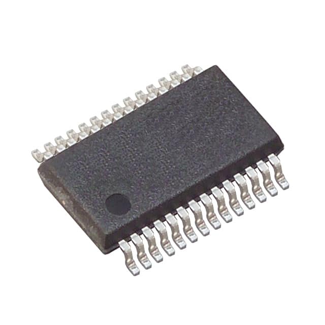
ICGOO在线商城 > ADS8515IBDB
- 型号: ADS8515IBDB
- 制造商: Texas Instruments
- 库位|库存: xxxx|xxxx
- 要求:
| 数量阶梯 | 香港交货 | 国内含税 |
| +xxxx | $xxxx | ¥xxxx |
查看当月历史价格
查看今年历史价格
ADS8515IBDB产品简介:
ICGOO电子元器件商城为您提供ADS8515IBDB由Texas Instruments设计生产,在icgoo商城现货销售,并且可以通过原厂、代理商等渠道进行代购。 提供ADS8515IBDB价格参考¥71.43-¥119.71以及Texas InstrumentsADS8515IBDB封装/规格参数等产品信息。 你可以下载ADS8515IBDB参考资料、Datasheet数据手册功能说明书, 资料中有ADS8515IBDB详细功能的应用电路图电压和使用方法及教程。
| 参数 | 数值 |
| 产品目录 | 集成电路 (IC)半导体 |
| 描述 | IC ADC 16BIT 250KSPS SAMP 28SSOP模数转换器 - ADC Bipolar Input 16-Bit 350KSPS |
| 产品分类 | |
| 品牌 | Texas Instruments |
| 产品手册 | |
| 产品图片 |
|
| rohs | 符合RoHS无铅 / 符合限制有害物质指令(RoHS)规范要求 |
| 产品系列 | 数据转换器IC,模数转换器 - ADC,Texas Instruments ADS8515IBDB- |
| 数据手册 | |
| 产品型号 | ADS8515IBDB |
| 产品培训模块 | http://www.digikey.cn/PTM/IndividualPTM.page?site=cn&lang=zhs&ptm=13240 |
| 产品目录页面 | |
| 产品种类 | 模数转换器 - ADC |
| 位数 | 16 |
| 供应商器件封装 | 28-SSOP |
| 信噪比 | 92 dB |
| 其它名称 | 296-21985-5 |
| 分辨率 | 16 bit |
| 包装 | 管件 |
| 单位重量 | 208.400 mg |
| 商标 | Texas Instruments |
| 安装类型 | 表面贴装 |
| 安装风格 | SMD/SMT |
| 封装 | Tube |
| 封装/外壳 | 28-SSOP(0.209",5.30mm 宽) |
| 封装/箱体 | SSOP-28 |
| 工作温度 | -40°C ~ 85°C |
| 工作电源电压 | 1.65 V to 5.25 V |
| 工厂包装数量 | 50 |
| 接口类型 | Parallel |
| 数据接口 | 并联 |
| 最大功率耗散 | 125 mW |
| 最大工作温度 | + 85 C |
| 最小工作温度 | - 40 C |
| 标准包装 | 50 |
| 特性 | - |
| 电压参考 | Internal, External |
| 电压源 | 模拟和数字 |
| 结构 | SAR |
| 转换器数 | 1 |
| 转换器数量 | 1 |
| 转换速率 | 250 kS/s |
| 输入数和类型 | 1 个单端,双极 |
| 输入类型 | Single-Ended |
| 通道数量 | 1 Channel |
| 采样率(每秒) | 250k |

.jpg)



- 商务部:美国ITC正式对集成电路等产品启动337调查
- 曝三星4nm工艺存在良率问题 高通将骁龙8 Gen1或转产台积电
- 太阳诱电将投资9.5亿元在常州建新厂生产MLCC 预计2023年完工
- 英特尔发布欧洲新工厂建设计划 深化IDM 2.0 战略
- 台积电先进制程称霸业界 有大客户加持明年业绩稳了
- 达到5530亿美元!SIA预计今年全球半导体销售额将创下新高
- 英特尔拟将自动驾驶子公司Mobileye上市 估值或超500亿美元
- 三星加码芯片和SET,合并消费电子和移动部门,撤换高东真等 CEO
- 三星电子宣布重大人事变动 还合并消费电子和移动部门
- 海关总署:前11个月进口集成电路产品价值2.52万亿元 增长14.8%


.jpg)
PDF Datasheet 数据手册内容提取
ADS8515 www.ti.com SLAS460D–JUNE2007–REVISEDSEPTEMBER2010 16-Bit 250-kSPS Sampling CMOS ANALOG-TO-DIGITAL CONVERTER CheckforSamples:ADS8515 FEATURES DESCRIPTION 1 • Standard±10-VInputRange The ADS8515 is a complete 16-bit sampling 2 • 90-dBMinSNRwith20-kHzInput analog-to-digital (A/D) converter using state-of-the-art CMOS structures. It contains a complete 16-bit, • ±2.0LSBMaxINL capacitor-based, SAR A/D converter with sample and • ±1LSBMaxDNL,16Bits,NoMissingCode hold (S/H), reference, clock, interface for • 5-VAnalogSupply,FlexibleI/OSupplyVoltage microprocessoruse,and3-stateoutputdrivers. at1.65Vto5.25V The ADS8515 is specified at a 250-kHz sampling rate • Pin-CompatiblewithADS7805/10(LowSpeed), over the full temperature range. Precision resistors and12-BitADS7804/8504 provide an industry standard ±10-V input range, while • UsesInternalorExternalReference the innovative design allows operation from a single +5-Vsupply,withpowerdissipationunder100mW. • FullParallelDataOutput The ADS8515 is available in a 28-pin SSOP package • 100-mWTypPowerDissipationat250kSPS and is fully specified for operation over the industrial • 28-PinSSOPPackage –40°Cto85°Ctemperaturerange. APPLICATIONS • IndustrialProcessControl • DataAcquisitionSystems • DigitalSignalProcessing • MedicalEquipment • Instrumentation R/C Clock Successive Approximation Register and Control Logic CS BYTE BUSY CDAC Output 7 kW Latches Three ± 10 V Input and State Three Parallel 2 kW 25.67 kW State Data Comparator Drivers Bus CAP Buffer Internal +4.096 V Ref 4 kW REF 1 Pleasebeawarethatanimportantnoticeconcerningavailability,standardwarranty,anduseincriticalapplicationsofTexas Instrumentssemiconductorproductsanddisclaimerstheretoappearsattheendofthisdatasheet. Alltrademarksarethepropertyoftheirrespectiveowners. 2 PRODUCTIONDATAinformationiscurrentasofpublicationdate. Copyright©2007–2010,TexasInstrumentsIncorporated Products conform to specifications per the terms of the Texas Instruments standard warranty. Production processing does not necessarilyincludetestingofallparameters.
ADS8515 SLAS460D–JUNE2007–REVISEDSEPTEMBER2010 www.ti.com This integrated circuit can be damaged by ESD. Texas Instruments recommends that all integrated circuits be handled with appropriateprecautions.Failuretoobserveproperhandlingandinstallationprocedurescancausedamage. ESDdamagecanrangefromsubtleperformancedegradationtocompletedevicefailure.Precisionintegratedcircuitsmaybemore susceptibletodamagebecauseverysmallparametricchangescouldcausethedevicenottomeetitspublishedspecifications. PACKAGE/ORDERINGINFORMATION(1) MINIMUM NO MINIMUM SPECIFIED INL MISSING SINAD TEMPERATURE PACKAGE- PACKAGE ORDERING TRANSPORT PRODUCT (LSB) CODE (dB) RANGE LEAD DESIGNATOR NUMBER MEDIA,QTY ADS8515IBDB Tube,50 ADS8515IB ±2 16Bits 89 –40°Cto85°C SSOP-28 DB ADS8515IBDBR TapeandReel,2000 ADS8515IDB Tube,50 ADS8515I ±3 16Bits 87 –40°Cto85°C SSOP-28 DB ADS8515IDBR TapeandReel,2000 (1) Forthemostcurrentpackageandorderinginformation,seethePackageOptionAddendumattheendofthisdocument,orseethe ADS8515productfolderatwww.ti.com. ABSOLUTE MAXIMUM RATINGS(1)(2) Overoperatingfree-airtemperaturerange(unlessotherwisenoted) ADS8515 V ±25V IN Analoginputs CAP +V +0.3VtoAGND2–0.3V ANA REF IndefiniteshorttoAGND2,momentaryshorttoV ANA DGND,AGND1,AGND2 ±0.3V Groundvoltagedifferences V 6V ANA V 6V DIG Digitalinputs –0.3Vto+V +0.3V DIG Maximumjunctiontemperature 165°C Internalpowerdissipation 825mW (1) StressesbeyondthoselistedunderAbsoluteMaximumRatingsmaycausepermanentdamagetothedevice.Thesearestressratings only,andfunctionaloperationofthedeviceattheseoranyotherconditionsbeyondthoseindicatedunderRecommendedOperating Conditionsisnotimplied.Exposuretoabsolute-maximum-ratedconditionsforextendedperiodsmayaffectdevicereliability. (2) Allvoltagevaluesarewithrespecttonetworkgroundterminal. 2 SubmitDocumentationFeedback Copyright©2007–2010,TexasInstrumentsIncorporated ProductFolderLink(s):ADS8515
ADS8515 www.ti.com SLAS460D–JUNE2007–REVISEDSEPTEMBER2010 ELECTRICAL CHARACTERISTICS AtT =–40°Cto85°C,f =250kHz,V =V =5V,andusinginternalreference(unlessotherwisenoted). A s DIG ANA ADS8515I ADS8515IB PARAMETER TESTCONDITIONS UNIT MIN TYP MAX MIN TYP MAX Resolution 16 16 Bits ANALOGINPUT Voltagerange ±10 ±10 V Impedance 8.885 8.885 kΩ Capacitance 75 75 pF THROUGHPUTSPEED Conversioncycletime Acquireandconvert 4 4 ms Throughputrate 250 250 kHz DCACCURACY INL Integrallinearityerror –3 3 –2 2 LSB(1) DNL Differentiallinearityerror –1 2 –1 1 LSB(1) Nomissingcodes 16 16 Bits Transitionnoise(2) 0.67 0.67 LSB Full-scaleerror(3)(4) Int.Ref. –0.5 0.5 –0.25 0.25 %FSR Full-scaleerrordrift Int.Ref. ±7 ±7 ppm/°C Full-scaleerror(3)(4) Ext.4.096-VRef. –0.25 0.25 –0.1 0.1 %FSR Full-scaleerrordrift Ext.4.096-VRef. ±2 ±2 ppm/°C Bipolarzeroerror(3) –4 4 –2 2 mV Bipolarzeroerrordrift ±2 ±2 ppm/°C Powersupplysensitivity (VDIG=VANA=VD) +4.75V<VD<+5.25V –8 8 –8 8 LSB ACACCURACY SFDR Spurious-freedynamicrange fI=20kHz 95 102 97 102 dB(5) THD Totalharmonicdistortion fI=20kHz –100 –94 –100 –96 dB SINAD Signal-to-(noise+distortion) fI=20kHz 87 91 89 91 dB –60-dBInput 30 32 dB SNR Signal-to-noiseratio fI=20kHz 88 92 90 92 dB Full-powerbandwidth(6) 500 500 kHz SAMPLINGDYNAMICS Aperturedelay 5 5 ns Transientresponse FSStep 2 2 ms Overvoltagerecovery(7) 150 150 ns REFERENCE Internalreferencevoltage 4.076 4.096 4.116 4.076 4.096 4.116 V Internalreferencesourcecurrent(must 1 1 mA useexternalbuffer) Internalreferencedrift 8 8 ppm/°C Externalreferencevoltagerangefor 3.9 4.096 4.2 3.9 4.096 4.2 V specifiedlinearity Externalreferencecurrentdrain Ext.4.096-VRef. 100 100 mA DIGITALINPUTS Logiclevels VIL Low-levelinputvoltage VDIG=1.65V–5.25V –0.3 0.8 –0.3 0.35*VDIG V VIH High-levelinputvoltage VDIG=1.65V–5.25V 0.65*VDIG VDIG+0.3V 0.65*VDIG VDIG+0.3V V IIL Low-levelinputcurrent VIL=0V ±10 ±10 mA IIH High-levelinputcurrent VIH=5V ±10 ±10 mA DIGITALOUTPUTS (1) LSBmeansleastsignificantbit.Forthe16-bit,±10-VinputADS8515,oneLSBis305mV. (2) Typicalrmsnoiseatworstcasetransitionsandtemperatures. (3) AsmeasuredwithfixedresistorsshowninFigure22.Adjustabletozerowithexternalpotentiometer. (4) Full-scaleerroristheworstcaseof–full-scaleor+full-scaledeviationfromidealfirstandlastcodetransitions,dividedbythetransition voltage(notdividedbythefull-scalerange)andincludestheeffectofoffseterror. (5) AllspecificationsindBarereferredtoafull-scale±10-Vinput. (6) Full-powerbandwidthisdefinedasthefull-scaleinputfrequencyatwhichsignal-to-(noise+distortion)degradesto60dB,or10bitsof accuracy. (7) Recoverstospecifiedperformanceafter2xFSinputovervoltage. Copyright©2007–2010,TexasInstrumentsIncorporated SubmitDocumentationFeedback 3 ProductFolderLink(s):ADS8515
ADS8515 SLAS460D–JUNE2007–REVISEDSEPTEMBER2010 www.ti.com ELECTRICAL CHARACTERISTICS (continued) AtT =–40°Cto85°C,f =250kHz,V =V =5V,andusinginternalreference(unlessotherwisenoted). A s DIG ANA ADS8515I ADS8515IB PARAMETER TESTCONDITIONS UNIT MIN TYP MAX MIN TYP MAX Dataformat(parallel16bits) Datacoding(binarytwoscomplement) VOL Low-leveloutputvoltage ISINK=1.6mA 0.4 0.4 V VOH High-leveloutputvoltage ISOURCE=500mA 0.8×VDIG 0.8×VDIG V Leakagecurrent Hi-Zstate,VOUT=0VtoVDIG ±5 ±5 mA Outputcapacitance Hi-Zstate 15 15 pF DIGITALTIMING Busaccesstiming 83 83 ns Busrelinquishtiming 83 83 ns POWERSUPPLIES VDIG Digitalinputvoltage 1.65 5.25 1.65 5.25 V VIDAIGNA ADnigaitlaolgininppuuttcvuorrlteangte Mustbe≤VANA 4.75 0.51 5.215 4.75 0.51 5.251 mVA IANA Analoginputcurrent 20 25 20 25 mA Powerdissipation fS=250kHz 100 125 100 125 mW TEMPERATURERANGE Specifiedperformance –40 +85 –40 +85 °C Deratedperformance(8) –55 +125 –55 +125 °C Storage –65 +150 –65 +150 °C THERMALRESISTANCE(ΘJA) SSOP 67 67 °C/W (8) Theinternalreferencemaynotbestartedcorrectlybeyondtheindustrialtemperaturerange(–40°Cto+85°C);therefore,useofan externalreferenceisrecommended. PIN CONFIGURATION DBPACKAGE SSOP-28 (TOPVIEW) VIN 1 28 VDIG AGND1 2 27 VANA REF 3 26 BUSY CAP 4 25 CS AGND2 5 24 R/C D15 (MSB) 6 23 BYTE D14 7 22 D0 (LSB) D13 8 21 D1 D12 9 20 D2 D11 10 19 D3 D10 11 18 D4 D9 12 17 D5 D8 13 16 D6 DGND 14 15 D7 4 SubmitDocumentationFeedback Copyright©2007–2010,TexasInstrumentsIncorporated ProductFolderLink(s):ADS8515
ADS8515 www.ti.com SLAS460D–JUNE2007–REVISEDSEPTEMBER2010 PINDESCRIPTIONS PIN DIGITAL NAME NO. I/O DESCRIPTION AGND1 2 Analogground.Usedinternallyasgroundreferencepoint. AGND2 5 Analogground. Atthestartofaconversion,BUSYgoeslowandstayslowuntiltheconversionis BUSY 26 O completedandthedigitaloutputshavebeenupdated. BYTE 23 I Selects8mostsignificantbits(low)or8leastsignificantbits(high). CAP 4 Referencebuffercapacitor.2.2-mFtantalumcapacitortoground. CS 25 I InternallyORedwithR/C.IfR/Clow,afallingedgeonCSinitiatesanewconversion. DGND 14 Digitalground. Databit15.Mostsignificantbit(MSB)ofconversionresults.Hi-ZstatewhenCSishigh,or D15(MSB) 6 O whenR/Cislow. D14 7 O Databit14.Hi-ZstatewhenCSishigh,orwhenR/Cislow. D13 8 O Databit13.Hi-ZstatewhenCSishigh,orwhenR/Cislow. D12 9 O Databit12.Hi-ZstatewhenCSishigh,orwhenR/Cislow. D11 10 O Databit11.Hi-ZstatewhenCSishigh,orwhenR/Cislow. D10 11 O Databit10.Hi-ZstatewhenCSishigh,orwhenR/Cislow. D9 12 O Databit9.Hi-ZstatewhenCSishigh,orwhenR/Cislow. D8 13 O Databit8.Hi-ZstatewhenCSishigh,orwhenR/Cislow. D7 15 O Databit7.Hi-ZstatewhenCSishigh,orwhenR/Cislow. D6 16 O Databit6.Hi-ZstatewhenCSishigh,orwhenR/Cislow. D5 17 O Databit5.Hi-ZstatewhenCSishigh,orwhenR/Cislow. D4 18 O Databit4.Hi-ZstatewhenCSishigh,orwhenR/Cislow. D3 19 O Databit3.Hi-ZstatewhenCSishigh,orwhenR/Cislow. D2 20 O Databit2.Hi-ZstatewhenCSishigh,orwhenR/Cislow. D1 21 O Databit1.Hi-ZstatewhenCSishigh,orwhenR/Cislow. Databit0.Leastsignificantbit(LSB)ofconversionresults.Hi-ZstatewhenCSishigh,or D0(LSB) 22 O whenR/Cislow. WithCSlowandBUSYhigh,afallingedgeonR/Cinitiatesanewconversion.WithCS R/C 24 I low,arisingedgeonR/Cenablestheparalleloutput. REF 3 Referenceinput/output.2.2-mFtantalumcapacitortoground. Analogsupplyinput.Nominally+5V.Decoupletogroundwith0.1-mFceramicand10-mF V 27 ANA tantalumcapacitors. V 28 Digitalsupplyinput.Canbeconnecteddirectlytopin27. DIG V 1 Analoginput.SeeFigure24. IN Copyright©2007–2010,TexasInstrumentsIncorporated SubmitDocumentationFeedback 5 ProductFolderLink(s):ADS8515
ADS8515 SLAS460D–JUNE2007–REVISEDSEPTEMBER2010 www.ti.com TYPICAL CHARACTERISTICS SIGNAL-TO-NOISEAND TOTALHARMONICDISTORTION SIGNAL-TO-NOISERATIO DISTORTION vs vs vs INPUTFREQUENCY INPUTFREQUENCY INPUTFREQUENCY 100 95 95 B d on - dB 95 o - dB 90 ortion - 90 THD -Total Harmonic Distorti 78895050 SNR - Signal-to-Noise Rati 788505 D - Signal to Noise and Dist 788505 A 70 70 SIN 70 1 10 100 1000 1 10 100 1000 1 10 100 1000 fi- Input Frequency - kHz fi- input frequency - kHz fi- input frequency - kHz Figure1. Figure2. Figure3. SIGNAL-TO-NOISEAND SPURIOUSFREEDYNAMICRANGE SIGNAL-TO-NOISERATIO DISTORTION vs vs vs INPUTFREQUENCY FREE-AIRTEMPERATURE FREE-AIRTEMPERATURE 105 100 100 purious Free Dynamic Range18989055000 Signal-to-Noise Ratio - dB 88990505 ffsi== 2205 0k HKzSPS nal to Noise and Distortion - dB 88990505 ffsi== 2205 0k HKzSPS SFDR - S 75 SNR - 75 NAD - Sig 75 70 70 SI 70 1 10 100 1000 -55-40-25-10 5 2035 50 65 80 95110125 -55-40-25-10 5 20 35 50 65 80 95110125 fi- input frequency - kHz TA- Free-Air-Temperature -°C TA- Free-Air-Temperature -°C Figure4. Figure5. Figure6. SPURIOUSFREEDYNAMICRANGE TOTALHARMONICDISTORTION INTERNALREFERENCEVOLTAGE vs vs vs FREE-AIRTEMPERATURE FREE-AIRTEMPERATURE FREE-AIRTEMPERATURE B100 -70 4.1 FDR - Spurious Free Dynamic Range - d 7889950505 ffsi== 2205 0k HKzSPS THD - Total Harmonic Distortion - dB -----9988750505 ffsi== 2205 0k HKzSPS V- Internal Reference Voltage - VREF 444444444.........000000000999999999123456789 S 70 -100 4.09 -55-40-25-10 5 2035 50 65 80 95110125 -40 -25 -10 5 20 35 50 65 80 -55-40-25-10 5 2035 50 65 80 95110125 TA- Free-Air-Temperature -°C TA- Free-Air-Temperature -°C TA- Free-Air-Temperature -°C Figure7. Figure8. Figure9. 6 SubmitDocumentationFeedback Copyright©2007–2010,TexasInstrumentsIncorporated ProductFolderLink(s):ADS8515
ADS8515 www.ti.com SLAS460D–JUNE2007–REVISEDSEPTEMBER2010 TYPICAL CHARACTERISTICS (continued) BIPOLARZEROERROR NEGATIVEFULL-SCALEERROR NEGATIVEFULL-SCALEERROR vs vs vs FREE-AIRTEMPERATURE FREE-AIRTEMPERATURE FREE-AIRTEMPERATURE 5 0.25 0.1 4 R 0.2 Internal Reference R 0.08 External Reference BPZ - Bipolar Zero Error - mV ---3210123 Negative Full-Scale Error - %FS --0000-....001001..5555101 Negative Full-Scale Error - %FS ---000000......0000002466420 --54 NFS - -0-.02.52 NFS - -0-.00.18 -40 -25 -10 5 20 35 50 65 80 -40 -25 -10 5 20 35 50 65 80 -40 -25 -10 5 20 35 50 65 80 TA- Free-Air-Temperature -°C TA- Free-Air-Temperature -°C TA- Free-Air-Temperature -°C Figure10. Figure11. Figure12. POSITIVEFULL-SCALEERROR POSITIVEFULL-SCALEERROR SUPPLYCURRENT vs vs vs FREE-AIRTEMPERATURE FREE-AIRTEMPERATURE FREE-AIRTEMPERATURE 0.25 0.1 0.025 R 0.2 Internal Reference R 0.08 External Reference S S F F % 0.15 % 0.06 0.023 Full-Scale Error - -00.0.00.5105 Full-Scale Error - -000...0002240 pply Current - mA 00..001291 Positive -0-.01.51 Positive --00..0064 I- SuDD 0.017 FS - -0.2 FS - -0.08 P P -0.25 -0.1 0.015 -40 -25 -10 5 20 35 50 65 80 -40 -25 -10 5 20 35 50 65 80 -40 -25 -10 5 20 35 50 65 80 TA- Free-Air-Temperature -°C TA- Free-Air-Temperature -°C TA- Free-Air-Temperature -°C Figure13. Figure14. Figure15. HISTOGRAM 4500 4103 4000 3645 3500 3000 nt 2500 u o C 2000 1500 1000 500 335 0 0 109 0 0 0 65529 65531 65533 65535 65530 65532 65534 65536 Code Figure16. Copyright©2007–2010,TexasInstrumentsIncorporated SubmitDocumentationFeedback 7 ProductFolderLink(s):ADS8515
ADS8515 SLAS460D–JUNE2007–REVISEDSEPTEMBER2010 www.ti.com TYPICAL CHARACTERISTICS (continued) INL 2 1.5 1 0.5 b - ls 0 L N I -0.5 -1 -1.5 -2 0 10000 20000 30000 40000 50000 60000 70000 Code Figure17. DNL 2 1.5 1 b 0.5 s - l NL 0 D -0.5 -1 -1.5 -2 0 10000 20000 30000 40000 50000 60000 70000 Code Figure18. 8 SubmitDocumentationFeedback Copyright©2007–2010,TexasInstrumentsIncorporated ProductFolderLink(s):ADS8515
ADS8515 www.ti.com SLAS460D–JUNE2007–REVISEDSEPTEMBER2010 BASIC OPERATION Figure 19 shows a basic circuit to operate the ADS8515 with a full parallel data output. Taking R/C (pin 24) low for a minimum of 40 ns initiates a conversion. BUSY (pin 26) goes low and stays low until the conversion is completed and the output registers are updated. Data are output in binary twos complement with the MSB on pin 6.BUSYgoinghighcanbeusedtolatchthedata. The ADS8515 begins tracking the input signal at the end of the conversion. Allowing 4 ms between convert commandsassuresaccurateacquisitionofanewsignal. 1 28 2 27 + + +5V 0.1 m F 10 m F + 3 26 2.2 m F BUSY 4 25 2.2 m F + Convert Pulse 5 24 R/C D15 (MSB) 6 23 D14 7 22 D0 (LSB) 40 ns Min ADS8515 D13 8 21 D1 D12 9 20 D2 D11 10 19 D3 D10 11 18 D4 D9 12 17 D5 D8 13 16 D6 14 15 D7 Figure19. BasicOperation Copyright©2007–2010,TexasInstrumentsIncorporated SubmitDocumentationFeedback 9 ProductFolderLink(s):ADS8515
ADS8515 SLAS460D–JUNE2007–REVISEDSEPTEMBER2010 www.ti.com STARTING A CONVERSION The combination of CS (pin 25) and R/C (pin 24) held low for a minimum of 40 ns immediately puts the sample/hold of the ADS8515 in the hold state and starts conversion n. BUSY (pin 26) goes low and stays low untilconversionniscompletedandtheinternaloutputregisterhasbeenupdated. The ADS8515 begins tracking the input signal at the end of the conversion. Allowing 4 ms between convert commands assures accurate acquisition of a new signal. Refer to Table 1 for a summary of CS, R/C, and BUSY statesandFigure21,Figure22,andFigure23forthetimingdiagrams. CS and R/C are internally ORed and level triggered. There is no requirement regarding which input goes low first when initiating a conversion. If, however, it is critical that CS or R/C initiates conversion n, be sure the less criticalinputislowatleast10nspriortotheinitiatinginput. To reduce the number of control pins, CS can be tied low using R/C to control the read and convert modes. The paralleloutputbecomesactivewheneverR/Cgoeshigh.RefertotheReadingDatasection. Table1.ControlLineFunctionsforReadandConvert CS R/C BUSY OPERATION 1 X X None.DatabusisinHi-Zstate. ↓ 0 1 Initiatesconversionn.DatabusremainsinHi-Zstate. 0 ↓ 1 Initiatesconversionn.DatabusentersHi-Zstate. 0 1 ↑ Conversionncompleted.Validdatafromconversionnonthedatabus. ↓ 1 1 Enablesdatabuswithvaliddatafromconversionn. ↓ 1 0 Enablesdatabuswithvaliddatafromconversion–1 (1).Conversionninprogress. 0 ↑ 0 Enablesdatabuswithvaliddatafromconversion–1 (1).Conversionninprogress. 0 0 ↑ Newconversioninitiatedwithoutacquisitionofanewsignal.Dataisinvalid.CSand/orR/C mustbehighwhenBUSYgoeshigh. X X 0 Conversionninprogress. (1) SeeFigure21andFigure22forconstraintsondatavalidfromconversionn–1. READING DATA The ADS8515 outputs full or byte-reading parallel data in binary twos complement data output format. The parallel output is active when R/C (pin 24) is high and CS (pin 25) is low. Any other combination of CS and R/C 3-states the parallel output. Valid conversion data can be read in a full parallel, 16-bit word or two 8-bit bytes on pins 6 to 13 and pins 15 to 22. BYTE (pin 23) can be toggled to read both bytes within one conversion cycle. RefertoTable2foridealoutputcodesandFigure20forbitlocationsrelativetothestateofBYTE. Table2.IdealInputVoltagesandOutputCodes DIGITALOUTPUTBINARYTWOSCOMPLEMENT DESCRIPTION ANALOGINPUT BINARYCODE HEXCODE Full-scalerange ±10V Leastsignificantbit(LSB) 305mV Fullscale(10V–1LSB) 9.999695V 0111111111111111 7FFF Midscale 0V 0000000000000000 0000 OneLSBbelowmidscale –305mV 1111111111111111 FFFF –Fullscale –10V 1000000000000000 8000 10 SubmitDocumentationFeedback Copyright©2007–2010,TexasInstrumentsIncorporated ProductFolderLink(s):ADS8515
ADS8515 www.ti.com SLAS460D–JUNE2007–REVISEDSEPTEMBER2010 PARALLEL OUTPUT (After a Conversion) After conversion n is completed and the output registers have been updated, BUSY (pin 26) goes high. Valid data from conversion n are available on D15 to D0 (pins 6 to 13 and 15 to 22). BUSY going high can be used to latchthedata.RefertoTable3andFigure21,Figure22,andFigure23fortimingspecifications. PARALLEL OUTPUT (During a Conversion) After conversion n has been initiated, valid data from conversion –1 can be read and are valid up to t after the 2 start of conversion n. Do not attempt to read data from t after the start of conversion n until BUSY (pin 26) goes 2 high; this may result in reading invalid data. Refer to Table 3 and Figure 21, Figure 22, and Figure 23 for timing specifications. Note: For the best possible performance, data should not be read during a conversion. The switching noise of theasynchronousdatatransfercancausedigitalfeedthroughdegradingtheconverterperformance. The number of control lines can be reduced by tying CS low while using the falling edge of R/C to initiate conversionsandtherisingedgeofR/Ctoactivatetheoutputmodeoftheconverter.SeeFigure21. Table3.ConversionTiming SYMBOL DESCRIPTION MIN TYP MAX UNITS t Pulseduration,convert 40 ns w1 t Accesstime,datavalidafterR/Clow 0.8 1.2 ms a t Propagationdelaytime,BUSYfromR/Clow 6 20 ns pd t Pulseduration,BUSYlow 2 ms w2 t Delaytime,BUSYafterendofconversion 5 ns d1 t Delaytime,aperture 5 ns d2 t Conversiontime 2 ms conv t Acquisitiontime 2 ms acq t Disabletime,bus 10 15 83 ns dis t Delaytime,BUSYafterdatavalid 35 50 ns d3 t Validtime,previousdataremainsvalidafterR/Clow 1.5 2 ms v t +t Throughputtime 4 ms conv acq t Setuptime,R/CtoCS 10 ns su t Cycletimebetweenconversions 4 ms c t Enabletime,bus 10 15 30 ns en t Delaytime,BYTE 10 15 30 ns d4 BYTE LOW BYTE HIGH +5 V Bit 15 (MSB) 6 23 Bit 7 6 23 Bit 14 7 22 Bit 0 (LSB) Bit 6 7 22 Bit 8 ADS8515 ADS8515 Bit 13 8 21 Bit 1 Bit 5 8 21 Bit 9 Bit 12 9 20 Bit 2 Bit 4 9 20 Bit 10 Bit 11 10 19 Bit 3 Bit 3 10 19 Bit 11 Bit 10 11 18 Bit 4 Bit 2 11 18 Bit 12 Bit 9 12 17 Bit 5 Bit 1 12 17 Bit 13 Bit 8 13 16 Bit 6 Bit 0 (LSB) 13 16 Bit 14 14 15 Bit 7 14 15 Bit 15 (MSB) Figure20. BitLocationsRelativetoStateofBYTE(Pin23) Copyright©2007–2010,TexasInstrumentsIncorporated SubmitDocumentationFeedback 11 ProductFolderLink(s):ADS8515
ADS8515 SLAS460D–JUNE2007–REVISEDSEPTEMBER2010 www.ti.com tw1 R/C tc ta1 tw2 BUSY tpd td2 td1 MODE Acquire Convert Acquire Convert tconv tacq Previous Previous DATA BUS Hi−Z Not Valid Data Valid Hi−Z Data Valid Data Valid Data Valid tdis td3 tv Figure21. ConversionTimingwithOutputsEnabledafterConversion(CSTiedLow) tsu tsu tsu tsu R/C tw1 CS tpd tw2 BUSY td2 MODE Acquire Convert Acquire tconv DATA BUS Hi−Z State Data Valid Hi−Z State ten tdis Figure22. UsingCStoControlConversionandReadTiming tsu tsu R/C CS BYTE Pins 6 − 13 Hi−Z High Byte Low Byte Hi−Z ten td4 tdis Pins 15 − 22 Hi−Z Low Byte High Byte Hi−Z Figure23. UsingCSandBYTEtoControlDataBus 12 SubmitDocumentationFeedback Copyright©2007–2010,TexasInstrumentsIncorporated ProductFolderLink(s):ADS8515
ADS8515 www.ti.com SLAS460D–JUNE2007–REVISEDSEPTEMBER2010 ADC RESET The ADC reset function of the ADS8515 can be used to terminate the current conversion cycle. Bringing R/C low for at least 40 ns while BUSY is low will initiate the ADC reset. To initiate a new conversion, R/C must return to the high state and remain high long enough to acquire a new sample (see Table 3, t ) before going low to initiate c the next conversion sequence. In applications that do not monitor the BUSY signal, it is recommended that the ADCresetfunctionbeimplementedaspartofasysteminitializationsequence. INPUT RANGES The ADS8515 offers a standard ±10-V input range. Figure 24 shows the necessary circuit connections for the ADS8515 with and without hardware trim. Offset and full-scale error specifications are tested and specified with the fixed resistors shown in Figure 25(b). Full-scale error includes offset and gain errors measured at both +FS and–FS.AdjustmentsforoffsetandgainaredescribedintheCalibrationsectionofthisdatasheet. The offset and gain are adjusted internally to allow external trimming with a single supply. The external resistors compensate for this adjustment and can be left out if the offset and gain are corrected in software (refer to the Calibrationsection). The nominal input impedance of 6.35 kΩ results from the combination of the internal resistor network shown on the front page of the product data sheet. The input resistor divider network provides inherent overvoltage protection assured to at least ±25 V. The 1% resistors used for the external circuitry do not compromise the accuracyordriftoftheconverter.Theyhavelittleinfluencerelativetotheinternalresistors,andtightertolerances arenotrequired. The input signal must be referenced to AGND1. This minimizes the ground loop problem typical to analog designs. The analog signal should be driven by a low impedance source. A typical driving circuit using an OPA627orOPA132isshowninFigure24. +15 V 2.2 (cid:2)F 22 pF ADS8515 100 nF VIN GND 2 k(cid:1) Pin7 Pin1 2 k(cid:1) Vin Pin2 − REF OPA627 22 pF or 2.2 (cid:2)F OPA132 Pin6 + Pin3 AGND1 Pin4 GND CAP GND 2.2 (cid:2)F 2.2 (cid:2)F GND DGND 100 nF GND AGND2 −15V GND Figure24. TypicalDrivingCircuit(±10V,NoTrim) Copyright©2007–2010,TexasInstrumentsIncorporated SubmitDocumentationFeedback 13 ProductFolderLink(s):ADS8515
ADS8515 SLAS460D–JUNE2007–REVISEDSEPTEMBER2010 www.ti.com APPLICATION INFORMATION CALIBRATION The gain of the ADS8515 can be trimmed in software. To achieve optimum performance, several iterations may berequired. Hardware Calibration To calibrate the gain of the ADS8515, install the resistors and potentiometer as shown in Figure 25(a). The calibrationrangeisapproximately±100mV. Software Calibration TheoffsetandgainoftheADS8515iscalibratedwithsoftware.SeeFigure25(b)forthecircuitconnections. 1 1 ±10 V VIN ±10 V VIN 2 2 AGND1 AGND1 +5 V 2.2µF+ 3 2.2µF+ 3 REF REF 175 kΩ 4 4 20 kΩ CAP CAP Gain + + 30 kΩ 2.2µF 5 2.2µF 5 AGND2 AGND2 (a)±10 V With HardwareTrim (b)±10 V Without HardwareTrim Note: Use 1% metal film resistors. Figure25. CircuitDiagramForSoftwareTrim REFERENCE The ADS8515 can operate with its internal 4.096-V reference or an external reference. By applying an external reference to pin 5, the internal reference can be bypassed. The reference voltage at REF is buffered internally withtheoutputonCAP(pin4). The internal reference has an 8 ppm/°C drift (typical) and accounts for approximately 20% of the full-scale error (FSE=±0.5%forlowgrade,±0.25%forhighgrade). REF REF (pin 3) is an input for an external reference or the output for the internal 4.096-V reference. A 2.2-mF capacitor should be connected as close to the REF pin as possible. The capacitor and the output resistance of REF create a low-pass filter to bandlimit noise on the reference. Using a smaller value capacitor introduces more noisetothereferencedegradingtheSNRandSINAD.TheREFpinshouldnotbeusedtodriveexternalacordc loads. The range for the external reference is 3.9 V to 4.2 V and determines the actual LSB size. Increasing the referencevoltageincreasesthefull-scalerangeandtheLSBsizeoftheconverterwhichcanimprovetheSNR. 14 SubmitDocumentationFeedback Copyright©2007–2010,TexasInstrumentsIncorporated ProductFolderLink(s):ADS8515
ADS8515 www.ti.com SLAS460D–JUNE2007–REVISEDSEPTEMBER2010 CAP CAP (pin 4) is the output of the internal reference buffer. A 2.2-mF capacitor should be placed as close to the CAP pin as possible to provide optimum switching currents for the CDAC throughout the conversion cycle and compensation for the output of the internal buffer. Using a capacitor any smaller than 1 mF can cause the output buffer to oscillate and may not have sufficient charge for the CDAC. Capacitor values larger than 2.2 mF have little affect on improving performance. The ESR (equivalent series resistance) of these compensation capacitors is also critical. Keep the total ESR under 3 Ω. See the Typical Characteristics section for how the worst case INL isaffectedbyESR. The output of the buffer is capable of driving up to 2 mA of current to a dc load, but any external load from the CAP pin may degrade the linearity of the ADS8515. Using an external buffer allows the internal reference to be used for larger dc loads and ac loads. Do not attempt to directly drive an ac load with the output voltage on CAP. This causes performance degradation of the converter. The ESR (equivalent series resistance) of these compensation capacitors is also critical. Keep the total ESR under 3 Ω. See the Typical Characteristics section concerninghowESRaffectsperformance. LAYOUT POWER The analog power pin (V ) and digital power pin (V ) can be tied together from the same +5V power supply, ANA DIG or from two different power-supply sources. The ADS8515 uses 90% of its power from the analog circuitry, and therefore should be considered as an analog component. Care must be taken to ensure that both the analog and digital power supplies power on before any voltage is applied to the analog input pin. Failure to do so may create alatch-upcondition.ThereisnopowersequencingrequirementbetweenV andV . ANA DIG GROUNDING Three ground pins are present on the ADS8515. DGND is the digital supply ground. AGND2 is the analog supply ground. AGND1 is the ground which all analog signals internal to the A/D converter are referenced. AGND1 is more susceptible to current induced voltage drops and must have the path of least resistance back to the power supply. All the ground pins of the A/D converter should be tied to the analog ground plane, separated from the system digital logic ground, to achieve optimum performance. Both analog and digital ground planes should be tied to the system ground as near to the power supplies as possible. This helps to prevent dynamic digital ground currentsfrommodulatingtheanaloggroundthroughacommonimpedancetopowerground. SIGNAL CONDITIONING The FET switches used for the sample hold on many CMOS A/D converters release a significant amount of charge injection which can cause the driving op amp to oscillate. The FET switch on the ADS8515, compared to the FET switches on other CMOS A/D converters, releases 5% to 10% of the charge. There is also a resistive front end which attenuates any charge which is released. The end result is a minimal requirement for the antialias filter on the front end. Any op amp sufficient for the signal in an application is sufficient to drive the ADS8515. The resistive front end of the ADS8515 also provides an assured ±25-V overvoltage protection. In most cases, thiseliminatestheneedforexternalinputprotectioncircuitry. INTERMEDIATE LATCHES The ADS8515 does have 3-state outputs for the parallel port, but intermediate latches should be used if the bus is to be active during conversions. If the bus is not active during conversion, the 3-state outputs can be used to isolate the A/D converter from other peripherals on the same bus. The 3-state outputs can also be used when theA/Dconverteristheonlyperipheralonthedatabus. Intermediate latches are beneficial on any monolithic A/D converter. The ADS8515 has an internal LSB size of 38 mV. Transients from fast switching signals on the parallel port, even when the A/D converter is 3-stated, can becoupledthroughthesubstratetotheanalogcircuitrycausingdegradationofconverterperformance. Copyright©2007–2010,TexasInstrumentsIncorporated SubmitDocumentationFeedback 15 ProductFolderLink(s):ADS8515
ADS8515 SLAS460D–JUNE2007–REVISEDSEPTEMBER2010 www.ti.com REVISION HISTORY NOTE:Pagenumbersforpreviousrevisionsmaydifferfrompagenumbersinthecurrentversion. ChangesfromRevisionC(August2010)toRevisionD Page • DeletedrowfromAbsoluteMaximumRatingsregardingV toV ................................................................................. 2 DIG ANA • DeletedtextregardingV fromthepin28descriptioninthePinDescriptiontable .......................................................... 5 ANA • ChangedtextinfirstandsecondsentencesofthePowersection ..................................................................................... 15 ChangesfromRevisionB(June2010)toRevisionC Page • Updateddocumentformattocurrentstandards ................................................................................................................... 1 • AddedtexttoendofPowersection .................................................................................................................................... 15 16 SubmitDocumentationFeedback Copyright©2007–2010,TexasInstrumentsIncorporated ProductFolderLink(s):ADS8515
PACKAGE OPTION ADDENDUM www.ti.com 6-Feb-2020 PACKAGING INFORMATION Orderable Device Status Package Type Package Pins Package Eco Plan Lead/Ball Finish MSL Peak Temp Op Temp (°C) Device Marking Samples (1) Drawing Qty (2) (6) (3) (4/5) ADS8515IBDB ACTIVE SSOP DB 28 50 Green (RoHS NIPDAU Level-2-260C-1 YEAR -40 to 85 ADS8515I & no Sb/Br) B ADS8515IBDBR ACTIVE SSOP DB 28 2000 Green (RoHS NIPDAU Level-2-260C-1 YEAR -40 to 85 ADS8515I & no Sb/Br) B ADS8515IBDBRG4 ACTIVE SSOP DB 28 2000 Green (RoHS NIPDAU Level-2-260C-1 YEAR -40 to 85 ADS8515I & no Sb/Br) B ADS8515IDB ACTIVE SSOP DB 28 50 Green (RoHS NIPDAU Level-2-260C-1 YEAR -40 to 85 ADS8515I & no Sb/Br) ADS8515IDBR ACTIVE SSOP DB 28 2000 Green (RoHS NIPDAU Level-2-260C-1 YEAR -40 to 85 ADS8515I & no Sb/Br) (1) The marketing status values are defined as follows: ACTIVE: Product device recommended for new designs. LIFEBUY: TI has announced that the device will be discontinued, and a lifetime-buy period is in effect. NRND: Not recommended for new designs. Device is in production to support existing customers, but TI does not recommend using this part in a new design. PREVIEW: Device has been announced but is not in production. Samples may or may not be available. OBSOLETE: TI has discontinued the production of the device. (2) RoHS: TI defines "RoHS" to mean semiconductor products that are compliant with the current EU RoHS requirements for all 10 RoHS substances, including the requirement that RoHS substance do not exceed 0.1% by weight in homogeneous materials. Where designed to be soldered at high temperatures, "RoHS" products are suitable for use in specified lead-free processes. TI may reference these types of products as "Pb-Free". RoHS Exempt: TI defines "RoHS Exempt" to mean products that contain lead but are compliant with EU RoHS pursuant to a specific EU RoHS exemption. Green: TI defines "Green" to mean the content of Chlorine (Cl) and Bromine (Br) based flame retardants meet JS709B low halogen requirements of <=1000ppm threshold. Antimony trioxide based flame retardants must also meet the <=1000ppm threshold requirement. (3) MSL, Peak Temp. - The Moisture Sensitivity Level rating according to the JEDEC industry standard classifications, and peak solder temperature. (4) There may be additional marking, which relates to the logo, the lot trace code information, or the environmental category on the device. (5) Multiple Device Markings will be inside parentheses. Only one Device Marking contained in parentheses and separated by a "~" will appear on a device. If a line is indented then it is a continuation of the previous line and the two combined represent the entire Device Marking for that device. (6) Lead/Ball Finish - Orderable Devices may have multiple material finish options. Finish options are separated by a vertical ruled line. Lead/Ball Finish values may wrap to two lines if the finish value exceeds the maximum column width. Addendum-Page 1
PACKAGE OPTION ADDENDUM www.ti.com 6-Feb-2020 Important Information and Disclaimer:The information provided on this page represents TI's knowledge and belief as of the date that it is provided. TI bases its knowledge and belief on information provided by third parties, and makes no representation or warranty as to the accuracy of such information. Efforts are underway to better integrate information from third parties. TI has taken and continues to take reasonable steps to provide representative and accurate information but may not have conducted destructive testing or chemical analysis on incoming materials and chemicals. TI and TI suppliers consider certain information to be proprietary, and thus CAS numbers and other limited information may not be available for release. In no event shall TI's liability arising out of such information exceed the total purchase price of the TI part(s) at issue in this document sold by TI to Customer on an annual basis. Addendum-Page 2
PACKAGE MATERIALS INFORMATION www.ti.com 26-Feb-2019 TAPE AND REEL INFORMATION *Alldimensionsarenominal Device Package Package Pins SPQ Reel Reel A0 B0 K0 P1 W Pin1 Type Drawing Diameter Width (mm) (mm) (mm) (mm) (mm) Quadrant (mm) W1(mm) ADS8515IBDBR SSOP DB 28 2000 330.0 16.4 8.1 10.4 2.5 12.0 16.0 Q1 ADS8515IDBR SSOP DB 28 2000 330.0 16.4 8.1 10.4 2.5 12.0 16.0 Q1 PackMaterials-Page1
PACKAGE MATERIALS INFORMATION www.ti.com 26-Feb-2019 *Alldimensionsarenominal Device PackageType PackageDrawing Pins SPQ Length(mm) Width(mm) Height(mm) ADS8515IBDBR SSOP DB 28 2000 350.0 350.0 43.0 ADS8515IDBR SSOP DB 28 2000 350.0 350.0 43.0 PackMaterials-Page2
PACKAGE OUTLINE DB0028A SSOP - 2 mm max height SCALE 1.500 SMALL OUTLINE PACKAGE C 8.2 TYP 7.4 A 0.1 C PIN 1 INDEX AREA SEATING PLANE 26X 0.65 28 1 2X 10.5 8.45 9.9 NOTE 3 14 15 0.38 28X 0.22 5.6 0.15 C A B B 5.0 NOTE 4 2 MAX 0.25 (0.15) TYP SEE DETAIL A GAGE PLANE 0 -8 0.95 0.05 MIN 0.55 DETA 15AIL A TYPICAL 4214853/B 03/2018 NOTES: 1. All linear dimensions are in millimeters. Any dimensions in parenthesis are for reference only. Dimensioning and tolerancing per ASME Y14.5M. 2. This drawing is subject to change without notice. 3. This dimension does not include mold flash, protrusions, or gate burrs. Mold flash, protrusions, or gate burrs shall not exceed 0.15 mm per side. 4. This dimension does not include interlead flash. Interlead flash shall not exceed 0.25 mm per side. 5. Reference JEDEC registration MO-150. www.ti.com
EXAMPLE BOARD LAYOUT DB0028A SSOP - 2 mm max height SMALL OUTLINE PACKAGE 28X (1.85) SYMM (R0.05) TYP 1 28X (0.45) 28 26X (0.65) SYMM 14 15 (7) LAND PATTERN EXAMPLE EXPOSED METAL SHOWN SCALE: 10X SOLDER MASK METAL METAL UNDER SOLDER MASK OPENING SOLDER MASK OPENING EXPOSED METAL EXPOSED METAL 0.07 MAX 0.07 MIN ALL AROUND ALL AROUND NON-SOLDER MASK SOLDER MASK DEFINED DEFINED (PREFERRED) SOLDE15.000 R MASK DETAILS 4214853/B 03/2018 NOTES: (continued) 6. Publication IPC-7351 may have alternate designs. 7. Solder mask tolerances between and around signal pads can vary based on board fabrication site. www.ti.com
EXAMPLE STENCIL DESIGN DB0028A SSOP - 2 mm max height SMALL OUTLINE PACKAGE 28X (1.85) SYMM (R0.05) TYP 1 28X (0.45) 28 26X (0.65) SYMM 14 15 (7) SOLDER PASTE EXAMPLE BASED ON 0.125 mm THICK STENCIL SCALE: 10X 4214853/B 03/2018 NOTES: (continued) 8. Laser cutting apertures with trapezoidal walls and rounded corners may offer better paste release. IPC-7525 may have alternate design recommendations. 9. Board assembly site may have different recommendations for stencil design. www.ti.com
IMPORTANTNOTICEANDDISCLAIMER TI PROVIDES TECHNICAL AND RELIABILITY DATA (INCLUDING DATASHEETS), DESIGN RESOURCES (INCLUDING REFERENCE DESIGNS), APPLICATION OR OTHER DESIGN ADVICE, WEB TOOLS, SAFETY INFORMATION, AND OTHER RESOURCES “AS IS” AND WITH ALL FAULTS, AND DISCLAIMS ALL WARRANTIES, EXPRESS AND IMPLIED, INCLUDING WITHOUT LIMITATION ANY IMPLIED WARRANTIES OF MERCHANTABILITY, FITNESS FOR A PARTICULAR PURPOSE OR NON-INFRINGEMENT OF THIRD PARTY INTELLECTUAL PROPERTY RIGHTS. These resources are intended for skilled developers designing with TI products. You are solely responsible for (1) selecting the appropriate TI products for your application, (2) designing, validating and testing your application, and (3) ensuring your application meets applicable standards, and any other safety, security, or other requirements. These resources are subject to change without notice. TI grants you permission to use these resources only for development of an application that uses the TI products described in the resource. Other reproduction and display of these resources is prohibited. No license is granted to any other TI intellectual property right or to any third party intellectual property right. TI disclaims responsibility for, and you will fully indemnify TI and its representatives against, any claims, damages, costs, losses, and liabilities arising out of your use of these resources. TI’s products are provided subject to TI’s Terms of Sale (www.ti.com/legal/termsofsale.html) or other applicable terms available either on ti.com or provided in conjunction with such TI products. TI’s provision of these resources does not expand or otherwise alter TI’s applicable warranties or warranty disclaimers for TI products. Mailing Address: Texas Instruments, Post Office Box 655303, Dallas, Texas 75265 Copyright © 2020, Texas Instruments Incorporated

 Datasheet下载
