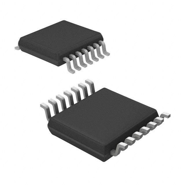
ICGOO在线商城 > ADS8513IDW
- 型号: ADS8513IDW
- 制造商: Texas Instruments
- 库位|库存: xxxx|xxxx
- 要求:
| 数量阶梯 | 香港交货 | 国内含税 |
| +xxxx | $xxxx | ¥xxxx |
查看当月历史价格
查看今年历史价格
ADS8513IDW产品简介:
ICGOO电子元器件商城为您提供ADS8513IDW由Texas Instruments设计生产,在icgoo商城现货销售,并且可以通过原厂、代理商等渠道进行代购。 提供ADS8513IDW价格参考¥52.46-¥87.48以及Texas InstrumentsADS8513IDW封装/规格参数等产品信息。 你可以下载ADS8513IDW参考资料、Datasheet数据手册功能说明书, 资料中有ADS8513IDW详细功能的应用电路图电压和使用方法及教程。
| 参数 | 数值 |
| 产品目录 | 集成电路 (IC)半导体 |
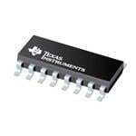
| 描述 | IC ADC 16BIT 40KSPS LP 16-SOIC模数转换器 - ADC 16B 40KSPS Lo Pwr Sampling ADC |
| 产品分类 | |
| 品牌 | Texas Instruments |
| 产品手册 | |
| 产品图片 |
|
| rohs | 符合RoHS无铅 / 符合限制有害物质指令(RoHS)规范要求 |
| 产品系列 | 数据转换器IC,模数转换器 - ADC,Texas Instruments ADS8513IDW- |
| 数据手册 | |
| 产品型号 | ADS8513IDW |
| 产品培训模块 | http://www.digikey.cn/PTM/IndividualPTM.page?site=cn&lang=zhs&ptm=13240 |
| 产品目录页面 | |
| 产品种类 | 模数转换器 - ADC |
| 位数 | 16 |
| 供应商器件封装 | 16-SOIC |
| 信噪比 | 89.9 dB |
| 其它名称 | 296-23166-5 |
| 分辨率 | 16 bit |
| 制造商产品页 | http://www.ti.com/general/docs/suppproductinfo.tsp?distId=10&orderablePartNumber=ADS8513IDW |
| 包装 | 管件 |
| 单位重量 | 420.400 mg |
| 商标 | Texas Instruments |
| 安装类型 | 表面贴装 |
| 安装风格 | SMD/SMT |
| 封装 | Tube |
| 封装/外壳 | 16-SOIC(0.295",7.50mm 宽) |
| 封装/箱体 | SOIC-16 |
| 工作温度 | -40°C ~ 85°C |
| 工作电源电压 | 2.7 V to 5.5 V |
| 工厂包装数量 | 40 |
| 接口类型 | QSPI, Serial, SPI |
| 数据接口 | 串行,并联 |
| 最大功率耗散 | 32.5 mW |
| 最大工作温度 | + 85 C |
| 最小工作温度 | - 40 C |
| 标准包装 | 40 |
| 特性 | - |
| 电压参考 | Internal, External |
| 电压源 | 单电源 |
| 系列 | ADS8513 |
| 结构 | SAR |
| 转换器数 | 1 |
| 转换器数量 | 1 |
| 转换速率 | 40 kS/s |
| 输入数和类型 | 3 个单端,单极3 个单端,双极 |
| 输入类型 | Single-Ended |
| 通道数量 | 1 Channel |
| 采样率(每秒) | 40k |




- 商务部:美国ITC正式对集成电路等产品启动337调查
- 曝三星4nm工艺存在良率问题 高通将骁龙8 Gen1或转产台积电
- 太阳诱电将投资9.5亿元在常州建新厂生产MLCC 预计2023年完工
- 英特尔发布欧洲新工厂建设计划 深化IDM 2.0 战略
- 台积电先进制程称霸业界 有大客户加持明年业绩稳了
- 达到5530亿美元!SIA预计今年全球半导体销售额将创下新高
- 英特尔拟将自动驾驶子公司Mobileye上市 估值或超500亿美元
- 三星加码芯片和SET,合并消费电子和移动部门,撤换高东真等 CEO
- 三星电子宣布重大人事变动 还合并消费电子和移动部门
- 海关总署:前11个月进口集成电路产品价值2.52万亿元 增长14.8%



PDF Datasheet 数据手册内容提取
ADS8513 www.ti.com...................................................................................................................................................... SLAS486C–JUNE2007–REVISEDJANUARY2009 16-Bit, 40kSPS, Low-Power Sampling ANALOG-TO-DIGITAL CONVERTER with Internal Reference and Parallel/Serial Interface FEATURES APPLICATIONS 1 • 40kSPSMinimumSamplingRate • IndustrialProcessControl 23 • VeryLowPower:24mWTyp • TestEquipment • ±3.33V,±5V,±10V,4V,and10VInputRanges • Robotics • 89dBSNRwith10kHzInput • DSPServoControl • ±2LSBMaxINL • MedicalInstrumentation • PortableDataAcquisitionSystems • –1/+2LSBMaxDNL,16-BitNMC • ±10mVBPZ,±2.5ppm/°CBPZDrift DESCRIPTION • 89dBMinSINAD,102dBMinSFDR The ADS8513 is a complete low-power, single 5V • UsesInternalorExternal2.5VReference supply, 16-bit sampling analog-to-digital (A/D) • NoExternalCalibrationResistorsRequired converter. It contains a complete 16-bit • Single5VAnalogSupply: capacitor-based, successive approximation register (SAR) A/D converter with sample and hold, clock, – 32.5mWMaxPowerDissipation reference, and serial data interface. The converter – 50m WMaxPower-DownMode can be configured for a variety of input ranges • SPI™-CompatibleSerialPortupto20MHz, including ±10V, ±5V, 0V to 10V, and 0.5V to 4.5V. A high-impedance, 0.3V to 2.8V input is also available withMaster/SlaveFeature with input impedance greater than 10MΩ. For most • GlobalCONVand3-StatedBusforMulti-Chip input ranges, the input voltage can swing to 25V or SimultaneousS/HOperation –25Vwithoutdamagetotheconverter. • Pin-Compatiblewith16-BitADS7813and An SPI-compatible serial interface allows data to be 12-BitADS7812andADS8512 synchronized to an internal or external clock. The • SO-16Package ADS8513 is specified at 40kSPS sampling rate over the–40°Cto+85°Cindustrialtemperaturerange. Successive Approximation Register Clock EXT/INT 40kW CDAC R1IN PWRD 8kW Serial BBUUSSYY R2IN Data CS Out 20kW CONV and R3IN Comparator Control SDATA DATACLK BUF CAP Buffer 4kW Internal REF +2.5 V Ref 1 Pleasebeawarethatanimportantnoticeconcerningavailability,standardwarranty,anduseincriticalapplicationsofTexas Instrumentssemiconductorproductsanddisclaimerstheretoappearsattheendofthisdatasheet. SPI,QSPIaretrademarksofMotorola,Inc. 2 Allothertrademarksarethepropertyoftheirrespectiveowners. 3 PRODUCTIONDATAinformationiscurrentasofpublicationdate. Copyright©2007–2009,TexasInstrumentsIncorporated Products conform to specifications per the terms of the Texas Instruments standard warranty. Production processing does not necessarilyincludetestingofallparameters.
ADS8513 SLAS486C–JUNE2007–REVISEDJANUARY2009...................................................................................................................................................... www.ti.com Thesedeviceshavelimitedbuilt-inESDprotection.Theleadsshouldbeshortedtogetherorthedeviceplacedinconductivefoam duringstorageorhandlingtopreventelectrostaticdamagetotheMOSgates. PACKAGE/ORDERINGINFORMATION(1) MINIMUM NO MINIMUM SPECIFIED INL MISSING SINAD TEMPERATURE PACKAGE PACKAGE ORDERING TRANSPORT PRODUCT (LSB) CODES (dB) RANGE LEAD DESIGNATOR NUMBER MEDIA,QTY ADS8513IBDW Tube,20 ADS8513IB ±2 16-Bit 89 –40°Cto+85°C SO-16 DW ADS8513IBDWR TapeandReel,1000 ADS8513IDW Tube,20 ADS8513I ±3 15-Bit 88 –40°Cto+85°C SO-16 DW ADS8513IDWR TapeandReel,1000 (1) Forthemostcurrentpackageandorderinginformation,seethePackageOptionAddendumattheendofthisdocument,orseetheTI websiteatwww.ti.com. ABSOLUTE MAXIMUM RATINGS(1)(2) overoperatingfree-airtemperaturerange(unlessotherwisenoted). PARAMETER UNIT R1 ±25V IN R2 ±25V IN Analoginputs R3 ±25V IN REF V +0.3VtoGND–0.3V S GND ±0.3V Groundvoltagedifferences V 6V S Digitalinputs –0.3Vto+V +0.3V S Maximumjunctiontemperature +165°C Storagetemperaturerange –65°Cto+150°C Internalpowerdissipation 700mW Leadtemperature(soldering,1,6mmfromcase10seconds) +260°C (1) StressesabovethoselistedunderAbsoluteMaximumRatingsmaycausepermanentdamagetothedevice.Exposuretoabsolute maximumconditionsforextendedperiodsmayaffectdevicereliability. (2) Allvoltagevaluesarewithrespecttonetworkgroundterminal. ELECTRICAL CHARACTERISTICS AtT =–40°Cto+85°C,f =40kSPS,V =5V,andusinginternalreferenceandfixedresistors,unlessotherwisespecified. A S S ADS8513I ADS8513IB PARAMETER TESTCONDITIONS MIN TYP MAX MIN TYP MAX UNIT Resolution 16 16 Bits ANALOGINPUT Voltageranges seeTable1 seeTable1 V Impedance seeTable1 seeTable1 Ω Capacitance 45 45 pF THROUGHPUTSPEED Conversiontime Acquireandconvert 20 20 m s Completecycle Acquireandconvert 25 25 m s Throughputrate Acquireandconvert 40 40 kSPS 2 SubmitDocumentationFeedback Copyright©2007–2009,TexasInstrumentsIncorporated ProductFolderLink(s):ADS8513
ADS8513 www.ti.com...................................................................................................................................................... SLAS486C–JUNE2007–REVISEDJANUARY2009 ELECTRICAL CHARACTERISTICS (continued) AtT =–40°Cto+85°C,f =40kSPS,V =5V,andusinginternalreferenceandfixedresistors,unlessotherwisespecified. A S S ADS8513I ADS8513IB PARAMETER TESTCONDITIONS MIN TYP MAX MIN TYP MAX UNIT DCACCURACY INL Integrallinearityerror –3 3 –2 2 LSB(1) DNL Differentiallinearityerror –2 3 –1 2 LSB Nomissingcodes 15 16 Bits Transitionnoise(2) 0.6 0.6 LSB Full-scaleerror(3)(4) –0.5 0.5 –0.25 0.25 % Full-scaleerrordrift 10 10 ppm/°C Full-scaleerror(3)(4) External2.5Vreference –0.5 0.5 –0.25 0.25 % Full-scaleerrordrift External2.5Vreference 0.2 0.2 ppm/°C Bipolarzeroerror(3) Bipolarranges –10 10 –10 10 mV Bipolarzeroerrordrift Bipolarranges 2.5 2.5 ppm/°C Unipolarzeroerror(3) Unipolarranges –6 6 –6 6 mV Unipolarzeroerrordrift Unipolarranges 2.5 2.5 ppm/°C Rpoewcoevredroywtinm(5e)toratedaccuracyfrom 1m FcapacitortoCAP 300 300 m s Power-supplysensitivity +4.75V<VS<+5.25V ±8 ±8 LSB ACACCURACY SFDR Spurious-freedynamicrange fIN=1kHz,±10V 90 100 96 102 dB(6) THD Totalharmonicdistortion fIN=1kHz,±10V –98 –90 –100 –96 dB fIN=1kHz,±10V 85 89 87 89 SINAD Signal-to-(noise+distortion) dB -60dBInput 30 32 SNR Signal-to-noise fIN=1kHz,±10V 85 89 87 89 dB Usablebandwidth(7) 130 130 kHz Full-powerbandwidth(–3dB) 600 600 kHz SAMPLINGDYNAMICS Aperturedelay 40 40 ns Aperturejitter 20 20 ps Transientresponse FSstep 5 5 m s Overvoltagerecovery(8) 750 750 ns REFERENCE Internalreferencevoltage Noload 2.48 2.5 2.52 2.48 2.5 2.52 V Internalreferencesourcecurrent(must 1 1 m A useexternalbuffer) Internalreferencedrift 8 8 ppm/°C Externalreferencevoltagerangefor 2.3 2.5 2.7 2.3 2.5 2.7 V specifiedlinearity Externalreferencecurrentdrain External2.5Vref 100 100 m A (1) LSBmeansLeastSignificantBit.1LSBforthe±10Vinputrangeis305m V. (2) Typicalrmsnoiseatworstcasetransitions. (3) Asmeasuredwithfixedresistors.Adjustabletozerowithexternalpotentiometer. (4) Full-scaleerroristheworstcaseof–FullScaleor+FullScaledeviationfromidealfirstandlastcodetransitions,dividedbythefull-scale range;includestheeffectofoffseterror.Testedat–40°Cto+85°C. (5) TimedelayaftertheADS8513isbroughtoutofPower-Downmodeuntilallinternalsettlingoccursandtheanaloginputisacquiredto ratedaccuracy.AConvertcommandafterthisdelaywillyieldaccurateresults. (6) AllspecificationsindBarereferredtoafull-scaleinput. (7) Usablebandwidthdefinedasfull-scaleinputfrequencyatwhichSignal-to-(Noise+Distortion)degradesto60dB. (8) Recoverstospecifiedperformanceafter2xFSinputovervoltage. Copyright©2007–2009,TexasInstrumentsIncorporated SubmitDocumentationFeedback 3 ProductFolderLink(s):ADS8513
ADS8513 SLAS486C–JUNE2007–REVISEDJANUARY2009...................................................................................................................................................... www.ti.com ELECTRICAL CHARACTERISTICS (continued) AtT =–40°Cto+85°C,f =40kSPS,V =5V,andusinginternalreferenceandfixedresistors,unlessotherwisespecified. A S S ADS8513I ADS8513IB PARAMETER TESTCONDITIONS MIN TYP MAX MIN TYP MAX UNIT DIGITALINPUTS VIL Low-levelinputvoltage –0.3 +0.8 –0.3 +0.8 V VIH High-levelinputvoltage 2.0 VD+0.3V 2.0 VD+0.3V V IIL Low-levelinputcurrent VIL=0V ±10 m A IIH High-levelinputcurrent VIH=5V ±10 m A DIGITALOUTPUTS Dataformat Serial Serial Datacoding Binarytwoscomplement Binarytwoscomplement VOL Low-leveloutputvoltage ISINK=1.6mA 0.4 0.4 V VOH High-leveloutputvoltage ISOURCE=500m A 4 4 V LeakageCurrent High-Zstate, ±1 ±1 m A VOUT=0VtoVS Outputcapacitance High-Zstate 15 15 pF DIGITALTIMING Busaccesstime RL=3.3kΩ,CL=50pF 83 83 ns Busrelinquishtime RL=3.3kΩ,CL=10pF 83 83 ns POWERSUPPLIES VS Supplyvoltage 4.75 5 5.25 4.75 5 5.25 V IDIG Digitalcurrent 0.6 0.6 mA IANA Analogcurrent 4.2 4.2 mA VS=5V,fS=40kSPS 24 32.5 24 32.5 mW Powerdissipation PWRDandREFDhigh 50 50 m W TEMPERATURERANGE Specifiedperformance –40 +85 –40 +85 °C Deratedperformance –55 +125 –55 +125 °C Storagetemperature –65 +150 –65 +150 °C q JA Thermalresistance 46 46 °C/W Table1. InputRanges CONNECTR1 CONNECTR2 CONNECTR3 INPUTIMPEDANCE IN IN IN ANALOGINPUTRANGE TO TO TO (kΩ) ±10V V BUF GND 45.7 IN 0.3125Vto2.8125V V V V >10,000 IN IN IN ±5V GND BUF V 26.7 IN 0Vto10V BUF GND V 26.7 IN 0Vto4V BUF V GND 21.3 IN ±3.33V V BUF V 21.3 IN IN 0.5Vto4.5V GND V GND 21.3 IN 4 SubmitDocumentationFeedback Copyright©2007–2009,TexasInstrumentsIncorporated ProductFolderLink(s):ADS8513
ADS8513 www.ti.com...................................................................................................................................................... SLAS486C–JUNE2007–REVISEDJANUARY2009 PIN CONFIGURATION DWPACKAGE SO-16 (TOPVIEW) R1IN 1 16 VS GND 2 15 PWRD R2IN 3 14 BUSY R3IN 4 13 CS BUF 5 12 CONV CAP 6 11 EXT/INT REF 7 10 DATA GND 8 9 DATACLK PinAssignments PIN DIGITAL NAME NO. I/O DESCRIPTION R1 1 Analoginput.SeeTable1andTable3. IN R2 3 Analoginput.SeeTable1andTable3. IN R3 4 Analoginput.SeeTable1andTable3. IN BUF 5 Referencebufferoutput.ConnecttoR1 ,R2 ,orR3 asneeded IN IN IN 6 Referencebuffercompensationnode.Decoupletogroundwitha1-m Ftantalumcapacitorinparallel CAP witha0.01m Fceramiccapacitor. 7 Referenceinput/output.Outputsinternal2.5Vreferenceviaaseries4kΩresistor.Decouplethis REF voltagewitha1m Fto2.2m Ftantalumcapacitortoground.Ifanexternalreferencevoltageisapplied tothispin,itoverridestheinternalreference. 9 I/O Dataclockpin.WithEXT/INTlow,thispinisanoutputandprovidesthesynchronousclockforthe DATACLK serialdata.Theoutputis3-statedwhenCSishigh.WithEXT/INThigh,thispinisaninputandthe serialdataclockmustbeprovidedexternally. 10 O Serialdataoutput.Theserialdataarealwaystheresultofthelastcompletedconversionandare DATA synchronizedtoDATACLK.IfDATACLKisfromtheinternalclock(EXT/INTlow),theserialdataare validonboththerisingandfallingedgesofDATACLK.DATAis3-statedwhenCSishigh. 11 I External/InternalDATACLKpin.Selectsthesourceofthesynchronousclockforserialdata.Ifhigh, theclockmustbeprovidedexternally.Iflow,theclockisderivedfromtheinternalconversionclock. EXT/INT Notethattheclockusedtotimetheconversionisalwaysinterna,lregardlessofthestatusof EXT/INT. 12 Convertinput.Afallingedgeonthisinputputstheinternalsample/holdintotheholdstateandstarts aconversionregardlessofthestateofCS.Ifaconversionisalreadyinprogress,thefallingedgeis CONV ignored.IfEXT/INTislow,datafromthepreviousconversionareseriallytransmittedduringthe currentconversion. 13 I Chipselect.Thisinput3-statesalloutputswhenhighandenablesalloutputswhenlow,including CS DATA,BUSY,andDATACLK(whenEXT/INTislow).NotethatafallingedgeonCONVinitiatesa conversionevenwhenCSishigh. 14 O Busyoutput.Whenaconversionstarts,BUSYgoeslowandremainslowthroughouttheconversion. BUSY IfEXT/INTislow,dataareseriallytransmittedwhileBUSYislow.BUSYis3-statedwhenCSis high. 15 I Power-downinput.Whenhigh,themajorityoftheADS8513circuitryisplacedinalow-powermode andpowerconsumptionissignificantlyreduced.(TheADS7813requiresCONVbetakenlowbefore PWRDgoeslowinordertoachievethelowestpowerconsumption.Thisisnotnecessaryforthe PWRD ADS8513anditdoesnotcauseinterferenceifperformed.)ThetimerequiredfortheADS7813to returntonormaloperationafterpowerdowndependsonanumberoffactors.ConsulttheChapter0 sectionformoreinformation. GND 2,8 Ground. 16 +5Vsupplyinput.Forbestperformance,decoupletogroundwitha0.1m Fceramiccapacitorin VS parallelwitha10m Ftantalumcapacitor. Copyright©2007–2009,TexasInstrumentsIncorporated SubmitDocumentationFeedback 5 ProductFolderLink(s):ADS8513
ADS8513 SLAS486C–JUNE2007–REVISEDJANUARY2009...................................................................................................................................................... www.ti.com TYPICAL CHARACTERISTICS POWER-SUPPLYCURRENT INTERNALREFERENCEVOLTAGE POWER-SUPPLYCURRENT vs vs vs FREE-AIRTEMPERATURE FREE-AIRTEMPERATURE SAMPLINGFREQUENCY 6 2.520 6 V 2.515 Power Supply Current - mA45..555 nternal Reference Voltage - 22222.....445559900105050 Power Supply Current - mA45..555 I- CC V- Iref2.485 I- CC 4 2.480 4 -40-25-10 5 20 35 50 65 80 95 110125 -40-25-10 5 20 35 50 65 80 95 110125 10 20 30 40 TA- Free-Air Temperature - ºC TA- Free-Air Temperature - ºC fs- Sampling Frequency - kHz Figure1. Figure2. Figure3. BIPOLARPOSITIVEFULL-SCALE BIPOLARNEGATIVEFULL-SCALE BIPOLAROFFSETERROR ERROR ERROR vs vs vs FREE-AIRTEMPERATURE FREE-AIRTEMPERATURE FREE-AIRTEMPERATURE OffsetError-mV 0369 2D0ri fVt =B 1ip.o5l aprp Rma/°nCge, Full-Scale Error - %FSR 0.00.510 2D0ri fVt =B 9ip.o2l aprp Rma/°nCge, e Full-Scale Error - %FSR 00..001.5501 2D0ri fVt =B 1ip2o.l2a rp Rpman/°gCe, Bipolar --63 Bipolar Positive -0-.00.51 Bipolar Negativ--00-..010.551 -45-30-15 0 15 30 45 60 75 90105120 -45-30-15 0 15 30 45 60 75 90105120 -45-30-15 0 15 30 45 60 75 90105120 TA- Free-Air Temperature -°C TA- Free-Air Temperature -°C TA- Free-Air Temperature -°C Figure4. Figure5. Figure6. BIPOLARPOSITIVEFULL-SCALE BIPOLARNEGATIVEFULL-SCALE BIPOLAROFFSETERROR ERROR ERROR vs vs vs FREE-AIRTEMPERATURE FREE-AIRTEMPERATURE FREE-AIRTEMPERATURE Bipolar Offset Error - mV-30369 1D0ri fVt =B 0ip.o8l aprp Rma/°nCge, olar Positive Full-Scale Error - %FSR 00..0001..55120 1D0ri fVt =B 1ip0o.l3a rp Rpman/°gCe, olar Negative Full-Scale Error - %FSR--000-...00100..555101 1D0ri fVt =B 1ip3o.l5a rp Rpman/°gCe, p p -6 Bi-0.05 Bi -0.2 -45-30-15 0 15 30 45 60 75 90105120 -45-30-15 0 15 30 45 60 75 90105120 -45-30-15 0 15 30 45 60 75 90105120 TA- Free-Air Temperature -°C TA- Free-Air Temperature -°C TA- Free-Air Temperature -°C Figure7. Figure8. Figure9. 6 SubmitDocumentationFeedback Copyright©2007–2009,TexasInstrumentsIncorporated ProductFolderLink(s):ADS8513
ADS8513 www.ti.com...................................................................................................................................................... SLAS486C–JUNE2007–REVISEDJANUARY2009 TYPICAL CHARACTERISTICS (continued) UNIPOLARPOSITIVEFULL-SCALE UNIPOLAROFFSETERROR ERROR UNIPOLAROFFSETERROR vs vs vs FREE-AIRTEMPERATURE FREE-AIRTEMPERATURE FREE-AIRTEMPERATURE 2 0.2 2 R 4D rVif tU =n 2ip.8o laprp mRa/°nCge, %FS 4D rVif tU =n 0ip.1o laprp mRa/°nCge, 1D0ri fVt =U 2n.i8p oplaprm R/°aCnge, Unipolar Offset Error - mV -101 ar Positive Full-Scale Error - Unipolar Offset Error - mV -011 ol p ni -2 U0.15 -2 -45-30-15 0 15 30 45 60 75 90105120 -45-30-15 0 15 30 45 60 75 90105120 -45-30-15 0 15 30 45 60 75 90105120 TA- Free-Air Temperature -°C TA- Free-Air Temperature -°C TA- Free-Air Temperature -°C Figure10. Figure11. Figure12. UNIPOLARPOSITIVEFULL-SCALE ERROR SPURIOUSFREEDYNAMICRANGE TOTALHARMONICDISTORTION vs vs vs FREE-AIRTEMPERATURE FREE-AIRTEMPERATURE FREE-AIRTEMPERATURE R 0.2 B110 -80 nipolar Positive Full-Scale Error - %FS 1D0ri fVt =U 0n.i4p oplaprm R/°aCnge, DR - Spurious Free Dynamic Range - d118990050505 fi= 10 kHz, 0 dB THD - Total Harmonic Distortion - dB--11---0099850505 fi= 10 kHz, 0 dB U 0.15 SF 80 -110 -45-30-15 0 15 30 45 60 75 90105120 -50 -25 0 25 50 75 100 125 -50 -25 0 25 50 75 100 125 TA- Free-Air Temperature -°C TA- Free-Air Temperature - ºC TA- Free-Air Temperature - ºC Figure13. Figure14. Figure15. SIGNAL-TO-NOISERATIO SIGNAL-TO-NOISE+DISTORTION SIGNAL-TO-NOISE+DISTORTION vs vs vs FREE-AIRTEMPERATURE FREE-AIRTEMPERATURE FREQUENCY SNR - Signal-To-Noise Ratio - dB 111189900050505 fi= 10 kHz, 0 dB AD - Signal-To-Noise + Distortion - dB 111189900050505 fi= 10 kHz, 0 dB AD - Signal-To-Noise + Distortion - dB1234567890000000000 --2060 0d dBdBB 80 SIN 80 SIN 10 -50 -25 0 25 50 75 100 125 -50 -25 0 25 50 75 100 125 0 2 4 6 8 10 12 14 16 18 20 TA- Free-Air Temperature - ºC TA- Free-Air Temperature - ºC f - Frequency - kHz Figure16. Figure17. Figure18. Copyright©2007–2009,TexasInstrumentsIncorporated SubmitDocumentationFeedback 7 ProductFolderLink(s):ADS8513
ADS8513 SLAS486C–JUNE2007–REVISEDJANUARY2009...................................................................................................................................................... www.ti.com TYPICAL CHARACTERISTICS (continued) SIGNAL-TO-NOISE+DISTORTION SIGNAL-TO-NOISERATIO SIGNAL-TO-NOISE+DISTORTION vs vs vs FREE-AIRTEMPERATURE FREQUENCY FREQUENCY 100 100 100 B f= 0 dB B D - Signal-To-Noise + Distortion - d 89890550 fsfi== 1100 kkHHfzzs, =0 2d0B kHfzs= 30 kHzfs= 40 kHz SNR - Signal-To-Noise Ratio - dB 789000 i D - Signal-To-Noise + Distortion - d 789000 fi= 0 dB A A SIN 75 600 1 10 100 1000 SIN 60 -50 -25 0 25 50 75 100 125 f - Frequency - kHz 0 1 10 100 1000 TA- Free-Air Temperature - ºC f - Frequency - kHz Figure19. Figure20. Figure21. SPURIOUSFREEDYNAMICRANGE TOTALHARMONICDISTORTION SPURIOUSFREEDYNAMICRANGE vs vs vs FREQUENCY FREQUENCY ESR B110 -70 B 110 d f= 0 dB d ange - i n - dB -80 fi= 0 dB ange - 105 fi= 10 kHz, 0 dB Dynamic R100 c Distortio -90 Dynamic R 100 R - Spurious Free 8900 HD - Total Harmoni--110100 R - Spurious Free 899505 D T D SF 70 -120 SF 80 0 1 10 100 1000 0 1 10 100 1000 0 1 2 3 4 5 6 7 8 9 10 f - Frequency - kHz f - Frequency - kHz ESR -W Figure22. Figure23. Figure24. TOTALHARMONICDISTORTION SIGNAL-TO-NOISERATIO SIGNAL-TO-NOISE+DISTORTION vs vs vs ESR ESR ESR -80 110 110 THD - Total Harmonic Distortion - dB --11---0099850505 fi= 10 kHz, 0 dB SNR - Signal-To-Noise Ratio - dB110089905505 fi= 10 kHz, 0 dB NAD - Signal-To-Noise + Distortion - dB110089950505 fi= 10 kHz, 0 dB -110 80 SI 80 0 1 2 3 4 5 6 7 8 9 10 0 1 2 3 4 5 6 7 8 9 10 0 1 2 3 4 5 6 7 8 9 10 ESR -W ESR -W ESR -W Figure25. Figure26. Figure27. 8 SubmitDocumentationFeedback Copyright©2007–2009,TexasInstrumentsIncorporated ProductFolderLink(s):ADS8513
ADS8513 www.ti.com...................................................................................................................................................... SLAS486C–JUNE2007–REVISEDJANUARY2009 TYPICAL CHARACTERISTICS (continued) OUTPUTREJECTION CONVERSIONTIME vs vs POWER-SUPPLYRIPPLE FREE-AIRTEMPERATURE FREQUENCY 17.8 -20 Silicon tested under -25 10 V Bipolar range s 17.7 μ e - dB -30 - Conversion TimRT111777...456 Output Rejection - ----54430505 VE -55 ON17.3 tC -60 17.2 -65 -50 -25 0 25 50 75 100 125 10 100 1k 10 k 100 k 1 M T - Free-Air Temperature - ºC Power Supply Ripple Frequency - Hz A Figure28. Figure29. INL 3 2 1 s B S L 0 - L N I -1 -2 -3 0 8192 16384 24576 32768 40960 49152 57344 65535 Code Figure30. DNL 3 2 1 s B S - L 0 L N D -1 -2 -3 0 8192 16384 24576 32768 40960 49152 57344 65535 Code Figure31. Copyright©2007–2009,TexasInstrumentsIncorporated SubmitDocumentationFeedback 9 ProductFolderLink(s):ADS8513
ADS8513 SLAS486C–JUNE2007–REVISEDJANUARY2009...................................................................................................................................................... www.ti.com TYPICAL CHARACTERISTICS (continued) FFT 0 -10 8192 Point FFT; f= 20 kHz, 0 dB i -20 -30 -40 B d-50 e - -60 d mplitu--8700 A-90 -100 -110 -120 -130 0 5 10 15 20 f - Frequency - kHz Figure32. FFT 0 -10 8192 Point FFT; f= 10 kHz, 0 dB i -20 -30 -40 B d -50 de - -60 u mplit --8700 A -90 -100 -110 -120 -130 0 5 10 15 20 f - Frequency - kHz Figure33. 10 SubmitDocumentationFeedback Copyright©2007–2009,TexasInstrumentsIncorporated ProductFolderLink(s):ADS8513
ADS8513 www.ti.com...................................................................................................................................................... SLAS486C–JUNE2007–REVISEDJANUARY2009 BASIC OPERATION INTERNAL DATACLK Figure 34 shows a basic circuit to operate the ADS8513 with a ±10V input range using an internal DATACLK. To begin a conversion and serial transmission of the results from the previous conversion, a falling edge must be provided to the CONV input. BUSY goes low to indicate that a conversion has started, and stays low until the conversion is complete. During the conversion, the results of the previous conversion are transmitted via DATA while DATACLK provides the synchronous clock for the serial data. The data format is 16-bit, binary twos complement, MSB first. Each data bit is valid on both the rising and falling edge of DATACLK. BUSY is low duringtheentireserialtransmissionandcanbeusedasaframesynchronizationsignal. C C ADS8513 1 2 0.1µF 10µF ±10V 1 R1IN VS 16 + +5V 2 GND PWRD 15 3 R2 BUSY 14 Frame Sync (optional) IN 4 R3 CS 13 IN 5 BUF CONV 12 Convert Pulse C + C 3 4 6 CAP EXT/INT 11 1µF 0.01µF C5 + 7 REF DATA 10 40ns min 1µF 8 GND DATACLK 9 Figure34.BasicOperatingCircuit,±10VInputRange,InternalDATACLK EXTERNAL DATACLK Figure 35 shows another basic circuit to operate the ADS8513 with a ±10V input rangeusing an external DATACLK. To begin a conversion, a falling edge must be provided to the CONV input. BUSY goes low to indicate that a conversion has started,and stays low until the conversion is complete. Just before BUSY rises near the end of the conversion, the conversion result held in the internal working register is transferred to the internalshiftregister. The internal shift register is clocked via the DATACLK input. The recommended method of reading the conversionresultistoprovidetheserialclockafter the conversion has completed. See External DATACLK under theReadingDatasectionofthisdatasheetformoreinformation. C C ADS8513 1 2 0.1µF 10µF ±10V 1 R1IN VS 16 + +5V 2 GND PWRD 15 3 R2 BUSY 14 Interrupt (optional) IN 4 R3 CS 13 Chip Select (optional(1)) IN Convert Pulse 5 BUF CONV 12 C + C 3 4 6 CAP EXT/INT 11 +5V 1µF 0.01µF C + 7 REF DATA 10 40ns min 5 1µF 8 GND DATACLK 9 External Clock NOTE: (1)TieCSto GND if the outputs will always be active. Figure35.BasicOperatingCircuit,±10VInputRange,ExternalDATACLK Copyright©2007–2009,TexasInstrumentsIncorporated SubmitDocumentationFeedback 11 ProductFolderLink(s):ADS8513
ADS8513 SLAS486C–JUNE2007–REVISEDJANUARY2009...................................................................................................................................................... www.ti.com STARTING A CONVERSION Ifa conversion is not currently in progress, a falling edge on the CONV input places the sample-and-hold into the hold mode and begins a conversion, as shown in Figure 36 according to the timing shown in Table 2. During the conversion, the CONV input is ignored. Starting a conversion does not depend on the state of CS. A conversion canbestartedonceevery25m s(40kSPSmaximumconversionrate).Thereisnominimumconversionrate. t 1 t 2 t t t 3 4 5 CONV t 6 t 7 BUSY t t 8 10 t9 t11 MODE Acquire Convert Acquire Convert Figure36.BasicConversionTiming Table2.ConversionandDataTiming,T =–40°Cto+85°C A SYMBOL DESCRIPTION MIN TYP MAX UNITS t Conversionplusacquisitiontime 25 m s 1 t CONVlowtoalldigitalinputsstable 19 m s 2 t CONVlowtoinitiateaconversion 0.04 12 m s 3 t BUSYrisingtoanydigitalinputactive 5 ns 4 t CONVhighpriortostartofconversion(CONVhightime) 15 ns 5 t BUSYlow 18 20 m s 6 t CONVlowtoBUSYlow 12 20 ns 7 t Aperturedelay(CONVfallingedgetoactualconversionstart) 5 ns 8 t Conversiontime 18 20 m s 9 t ConversioncompletetoBUSYrising 90 ns 10 t Acquisitiontime 7 m s 11 t CONVlowtorisingedgeoffirstinternalDATACLK 2.0 m s 12 t InternalDATACLKhigh 300 410 425 ns 13 t InternalDATACLKlow 300 410 425 ns 14 t InternalDATACLKperiod 0.6 0.82 0.85 m s 15 t DATAvalidtointernalDATACLKrising 150 204 ns 16 t InternalDATACLKfallingtoDATAnotvalid 150 208 ns 17 t FallingedgeoflastDATACLKtoBUSYrising 4.4 5 m s 18 t ExternalDATACLKrisingtoDATAnotvalid 4 14 ns 19 t ExternalDATACLKrisingtoDATAvalid 2 12 20 ns 20 t ExternalDATACLKhigh 15 ns 21 t ExternalDATACLKlow 15 ns 22 t ExternalDATACLKperiod 35 ns 23 t CONVlowtoexternalDATACLKactive 15 ns 24 t ExternalDATACLKloworCShightoBUSYrising 5 m s 25 t CSlowtodigitaloutputsenabled 15 ns 26 t CShightodigitaloutputsdisabled 15 ns 27 12 SubmitDocumentationFeedback Copyright©2007–2009,TexasInstrumentsIncorporated ProductFolderLink(s):ADS8513
ADS8513 www.ti.com...................................................................................................................................................... SLAS486C–JUNE2007–REVISEDJANUARY2009 Even though the CONV input is ignored while a conversion is in progress, this input should be held static during the conversion period. Transitions on this digital input can easily couple into sensitive analog portions of the converter, adversely affecting the conversion results (see the Sensitivity to External Digital Signals section of this datasheetformoreinformation). Ideally, the CONV input should go low and remain low throughout the conversion. It should return high sometime after BUSY goes high. In addition, it should be high before the start of the next conversion for a minimum time periodgivenbyt .ThisperiodensuresthatthedigitaltransitionontheCONVinputdoesnot affect the signal that 5 isacquiredforthenextconversion. An acceptable alternative is to return the CONV input high as soon after the start of the conversion as possible. For example, a negative-going pulse 100ns wide would make a good CONV input signal. It is strongly recommended that from time t after the start of a conversion until BUSY rises, the CONV input should be held 2 static(eitherhighorlow).Duringthistime,theconverterismoresensitivetoexternalnoise. Copyright©2007–2009,TexasInstrumentsIncorporated SubmitDocumentationFeedback 13 ProductFolderLink(s):ADS8513
ADS8513 SLAS486C–JUNE2007–REVISEDJANUARY2009...................................................................................................................................................... www.ti.com READING DATA The ADS8513 digital output is in Binary Two’s Complement (BTC) format. Table 3 shows the relationship betweenthedigitaloutputwordandtheanaloginputvoltageunderidealconditions. Table3.OutputCodesandIdealInputVoltages DESCRIPTION ANALOGINPUTRANGE DIGITALOUTPUT Full-scalerange ±10V 0.5Vto4.5V BINARYTWOSCOMPLEMENT Leastsignificantbit(LSB) 305m V 61m V BINARYCODE HEXCODE +Full-scale(FS–1LSB) 9.999695V 4.499939V 0111111111111111 7FFF Midscale 0V 2.5V 0000000000000000 0000 OneLSBbelowmidscale –305m V 2.499939m V 1111111111111111 FFFF –Full-scale –10V 0.5V 1000000000000000 8000 Figure 37 shows the relationship between the various digital inputs, digital outputs, and internal logic of the ADS8513. Figure 38 illustrates when the internal shift register of the ADS8513 is updated and how this update relates to a single conversion cycle. Together, these two figures define a very important aspect of the ADS8513: the conversion result is not available until after the conversion is complete. The implications of this protocolarediscussedinthefollowingsections. Converter Core REF CDAC CONV Clock Control Logic BUSY Each flip-flop in the working register is latched as the conversion proceeds Working Register D Q D Q D Q D Q D Q ••• W0 W1 W2 W14 W15 Update of the shift register occurs just prior toBUSYRising(1) Shift Register D Q D Q D Q D Q D Q D Q DATA EXT/INT S0 S1 S2 S14 S15 SOUT Delay DATACLK CS NOTE: (1) If EXT/INTis HIGH (external clock), DATACLK is HIGH, andCSis LOW during this time, the shift register will not be updated and the conversion result will be lost. Figure37.BlockDiagramoftheADS8513DigitalInputsandOutputs 14 SubmitDocumentationFeedback Copyright©2007–2009,TexasInstrumentsIncorporated ProductFolderLink(s):ADS8513
ADS8513 www.ti.com...................................................................................................................................................... SLAS486C–JUNE2007–REVISEDJANUARY2009 CONV t 25 t –t 6 25 BUSY NOTE: Update of the internal shift register occurs in the shaded region. If EXT/INTis HIGH, then DATACLK must be LOW or CS must be HIGH during this time. Figure38.ShiftRegisterUpdateTiming INTERNALDATACLK With EXT/INT tied low, the result from conversion ‘n’ is serially transmitted during conversion ‘n+1’, as shown in Figure 39 and with the timing given in Table 2. Serial transmission of data occurs only during a conversion. Whenatransmissionisnotinprogress,DATAandDATACLKarelow. t 1 CONV BUSY t 13 t t t 12 15 18 DATACLK 1 2 3 14 15 16 1 t t 16 14 t 17 DATA MSB Bit 14 Bit 13 Bit 2 Bit 1 LSB MSB Figure39.SerialDataTiming,InternalClock(EXT/INTandCSLow) During the conversion, the results of the previous conversion are transmitted via DATA, while DATACLK provides the synchronous clock for the serial data. The data format is 16-bit, Binary Two’s Complement, MSB first. Each data bit is valid on both the rising and falling edges of DATACLK. BUSY is low during the entire serial transmissionandcanbeusedasaframesynchronizationsignal. EXTERNALDATACLK With EXT/INT tied high, the result from conversion ‘n’ is clocked out after the conversion has completed, during the next conversion (‘n+1’), or a combination of these two. Figure 40 shows the case of reading the conversion result after the conversion is complete. Figure 41 describes reading the result during the next conversion. Figure 42 combines the important aspects of Figure 40 and Figure 41 for reading part of the result after the conversioniscompleteandthebalanceduringthenextconversion. The serial transmission of the conversion result is initiated by a rising edge on DATACLK. The data format is 16-bit, Binary Two’s Complement, MSB first. Each data bit is valid on the falling edge of DATACLK. In some cases, it might be possible to use the rising edge of the DATACLK signal. However, one extra clock period (not showninFigure40,Figure41,andFigure42)isneededforthefinalbit. The external DATACLK signal must be low or CS must be high before BUSY rises (see time t in Figure 41 and 25 Figure 42). If this limit is not observed during this time, the output shift register of the ADS8513 is not updated withtheconversionresult.Instead,thepreviouscontentsoftheshiftregisterremainandthenewresultislost. Copyright©2007–2009,TexasInstrumentsIncorporated SubmitDocumentationFeedback 15 ProductFolderLink(s):ADS8513
ADS8513 SLAS486C–JUNE2007–REVISEDJANUARY2009...................................................................................................................................................... www.ti.com Before reading the next three paragraphs, consult the Sensitivity to External Digital Signals section of this data sheet. This section explains many of the concerns regarding how and when to apply the external DATACLK signal. ExternalDATACLKActiveAftertheConversion The preferred method of obtaining the conversion result is to provide the DATACLK signal after the conversion has been completed and before the next conversion starts, as shown in Figure 40. Note that the DATACLK signal should be static before the start of the next conversion. If this limit is not observed, the DATACLK signal couldaffecttheacquired. t 1 t 5 CONV BUSY t 21 t t 4 23 DATACLK 1 2 3 4 14 15 16 t t 19 22 t 20 DATA MSB Bit 14 Bit 13 Bit 2 Bit 1 LSB Figure40.SerialDataTiming,ExternalClock,ClockingAftertheConversionCompletes(EXT/INTHigh, CSLow) ExternalDATACLKActiveDuringtheNextConversion Another method of obtaining the conversion result is shown in Figure 41. Because the output shift register is not updated until the end of the conversion, the previous result remains valid during the next conversion. If a fast clock(≥2MHz)canbeprovidedtotheADS8513,theresultcanbereadduringtimet .Duringthis time, the noise 2 fromtheDATACLKsignalislesslikelytoaffecttheconversionresult. t 1 t 2 CONV BUSY t 21 t t t 24 23 25 DATACLK 1 2 3 4 15 16 1 t t 19 22 t 20 DATA MSB Bit 14 Bit 13 Bit 1 LSB MSB Figure41.SerialDataTiming,ExternalClock,ClockingDuringtheNextConversion(EXT/INTHigh,CS Low) 16 SubmitDocumentationFeedback Copyright©2007–2009,TexasInstrumentsIncorporated ProductFolderLink(s):ADS8513
ADS8513 www.ti.com...................................................................................................................................................... SLAS486C–JUNE2007–REVISEDJANUARY2009 ExternalDATACLKActiveAftertheConversionandDuringtheNextConversion Figure 42 shows a method that combines the two previous approaches. This method works very well for microcontrollers that do serial transfers eight bits at a time and for slower microcontrollers. For example, if the fastestserialclockthatthemicrocontrollercanproduceis1m s,theapproachshowninFigure 40would result in a diminished throughput (26kSPS maximum conversion rate). The method described in Figure 41 could not be usedwithoutriskofaffectingtheconversionresult(theclockwouldhavetobeactiveaftertimet ).Therefore, the 2 approach in Figure 42 results in an improved throughput rate (33kSPS maximum with a 1m s clock), and DATACLKisnotactiveaftertimet . 2 CONV BUSY t 5 t t t 4 24 25 DATACLK 1 2 n n+1 15 16 DATA MSB Bit 14 Bit n Bit n-1 Bit 1 LSB Figure42.SerialDataTiming,ExternalClock,ClockingAftertheConversionCompletesandDuringthe NextConversion(EXT/INTHigh,CSLow) CHIP SELECT The CS input allows the digital outputs of the ADS8513 to be disabled and gates the external DATACLK signal when EXT/INT is high. See Figure 43 for the enable and disable time associated with CS and Figure 37 for a logicdiagramoftheADS8513.Thedigitaloutputscanbedisabledatanytime. Note that a conversion is initiated on the falling edge of CONV even if CS is high. If the EXT/INT input is low (internal DATACLK) and CS is high during the entire conversion, the previous conversion result is lost (that is, theserialtransmissionoccursbutDATAandDATACLKaredisabled). CS t t 26 27 BUSY, DATA, HI-Z Active HI-Z DATACLK(1) NOTE: (1) DATACLK is an output only when EXT/INTis LOW. Figure43.EnableandDisableTimingforDigitalOutputs Copyright©2007–2009,TexasInstrumentsIncorporated SubmitDocumentationFeedback 17 ProductFolderLink(s):ADS8513
ADS8513 SLAS486C–JUNE2007–REVISEDJANUARY2009...................................................................................................................................................... www.ti.com ANALOG INPUT The ADS8513 offers a number of input ranges. This set of options is accomplished by connecting the three input resistors to either the analog input (V ), to ground (GND), or to the 2.5V reference buffer output (BUF). Table 1 IN shows the input ranges that are typically used in most data acquisition applications. These ranges are all specified to meet the specifications given in the Electrical Characteristics table. Table 4 contains a complete list ofidealinputranges,associatedinputconnections,andcommentsregardingtherange. Table4.CompletelistofIdealInputRanges ANALOG CONNECT CONNECT CONNECT INPUT INPUT R1 R2 R3 IMPEDANCE IN IN IN RANGE(V) TO TO TO (kΩ) COMMENT 0.3125to2.8125 V V V >10,000 Specifiedoffsetandgain IN IN IN –0.417to2.916 V V BUF 26.7 V cannotgobelowGND–0.3V IN IN IN 0.417to3.750 V V GND 26.7 Offsetandgainnotspecified IN IN ±3.333 V BUF V 21.3 Specifiedoffsetandgain IN IN –15to5 V BUF BUF 45.7 Offsetandgainnotspecified IN ±10 V BUF GND 45.7 Specifiedoffsetandgain IN 0.833to7.5 V GND V 21.3 Offsetandgainnotspecified IN IN –2.5to17.5 V GND BUF 45.7 ExceedsabsolutemaximumV IN IN 2.5to22.5 V GND GND 45.7 ExceedsabsolutemaximumV IN IN 0to2.857 BUF V V 45.7 Offsetandgainnotspecified IN IN –1to3 BUF V BUF 21.3 V cannotgobelowGND–0.3V IN IN 0to4 BUF V GND 21.3 Specifiedoffsetandgain IN –6.25to3.75 BUF BUF V 26.7 Offsetandgainnotspecified IN 0to10 BUF GND V 26.7 Specifiedoffsetandgain IN 0.357to3.214 GND V V 45.7 Offsetandgainnotspecified IN IN –0.5to3.5 GND V BUF 21.3 V cannotgobelowGND–0.3V IN IN 0.5to4.5 GND V GND 21.3 Specifiedoffsetandgain IN ±5 GND BUF V 26.7 Specifiedoffsetandgain IN 1.25to11.25 GND GND V 26.7 Offsetandgainnotspecified IN +15 V 2.2(cid:2)F 22pF ADS8513 100nF R1IN GND 2k(cid:1) Pin7 Pin1 GND 2k(cid:1) VIN Pin2 − R2IN OPA627 22pF or OPA132 Pin6 + Pin3 R3IN Pin4 CAP GND 2.2(cid:2)F 2.2(cid:2)F REF GND 100nF 2.2(cid:2)F GND −15V GND Figure44.TypicalDrivingCircuit(±10V,NoTrim) 18 SubmitDocumentationFeedback Copyright©2007–2009,TexasInstrumentsIncorporated ProductFolderLink(s):ADS8513
ADS8513 www.ti.com...................................................................................................................................................... SLAS486C–JUNE2007–REVISEDJANUARY2009 The input impedance results from the various connections and the internal resistor values (refer to the block diagram on the front page of this data sheet). The internal resistor values are typical and can change by ±30% as a result of process variations. However, the ratio matching of the resistors is considerably better than this range. Thus, the input range only varies a few tenths of a percent from part to part, while the input impedance canvaryupto±30%. The Electrical Characteristics table contains the maximum limits for the variation of the analog input range, but only for those ranges where the comment field shows that the offset and gain are specified (including all the rangeslistedinTable1).Fortheotherranges,theoffsetandgainarenottestedandarenotspecified. Five of the input ranges in Table 4 are not recommended for general use. The upper-end of the –2.5V to +17.5V range and +2.5V to +22.5V range exceeds the absolute maximum analog input voltage. These ranges can still be used as long as the input voltage remains under the absolute maximum, but this limit may reduce the full-scalerangeoftheconvertertoasignificantdegree. Likewise, three of the input ranges involve the connection at R2 being driven below GND. This input has a IN reverse-biased ESD protection diode connection to ground. If R2 is taken below GND – 0.3V, this diode IN becomes forward-biased and clamps the negative input at –0.4V to –0.7V, depending on the temperature. Becausethenegativefull-scalevalueoftheseinputrangesexceeds–0.4V,theyarenotrecommended. Note that Table 4 assumes that the voltage at the REF pin is +2.5V. This assumption is true if the internal reference is used or if the external reference is +2.5V. Using other reference voltages change the values in Table4. HIGH IMPEDANCE MODE When R1 , R2 , and R3 are connected to the analog input, the input range of the ADS8513 is 0.3125V to IN IN IN 2.8125V and the input impedance is greater than 10MΩ. This input range can be used to connect the ADS8513 directly to a wide variety of sensors. Figure 45 shows the impedance of the sensor versus the change in integral linearity error (ILE) and differential linearity error (DLE) of the ADS8513. The performance of the ADS8513 can be improved for higher sensor impedance by allowing more time for acquisition. For example, 10m s of acquisition timeapproximatelydoublesthesensorimpedanceforthesameILE/DLEperformance. The input impedance and capacitance of the ADS8513 are very stable over temperature. Assuming that this performanceistrueofthesensoraswell,thegraphshownin Figure 45will vary less than a few percent over the ensured temperature range of the ADS8513. If the sensor impedance varies significantly with temperature, the worst-caseimpedanceshouldbeused. LINEARITYERROR vs SOURCE IMPEDANCE 10 9 T = +25°C A AcquisitionTime = 5µs 8 DLE aseBs) 7 CS Change in Worst-Linearity Error (L 6543 ILE 2 1 0 0 1 2 3 4 5 6 7 8 9 10 11 12 13 14 15 External Source Impedance (kΩ) Figure45.LinearityErrorvsSourceImpedanceintheHighImpedanceMode(R1 =R2 =R3 =V ) IN IN IN IN Copyright©2007–2009,TexasInstrumentsIncorporated SubmitDocumentationFeedback 19 ProductFolderLink(s):ADS8513
ADS8513 SLAS486C–JUNE2007–REVISEDJANUARY2009...................................................................................................................................................... www.ti.com DRIVING THE ADS8513 ANALOG INPUT In general, any reasonably fast, high-quality operational or instrumentation amplifier can be used to drive the ADS8513 input. When the converter enters the acquisition mode, there is some charge injection from the converter input to the amplifier output. This charge injection can result in inadequate settling time with slower amplifiers.Beverycarefulwithsingle-supply amplifiers, particularly if the output is required to swing very close to thesupplyrails. In addition, be careful with regard to the amplifier linearity. The outputs of single-supply and rail-to-rail amplifiers can saturate as the outputs approach the supply rails. Rather than the amplifier transfer function being a straight line, the curve can become severely S-shaped. Also, watch for the point where the amplifier switches from sourcing current to sinking current. For some amplifiers, the transfer function can be noticeably discontinuous at thispoint,causingasignificantchangeintheoutputvoltageforamuchsmallerchangeontheinput. Texas Instruments manufactures a wide variety of operational and instrumentation amplifiers that can be used to drivetheinputoftheADS8513;thesedevicesincludetheOPA627,OPA132,andINA110. 20 SubmitDocumentationFeedback Copyright©2007–2009,TexasInstrumentsIncorporated ProductFolderLink(s):ADS8513
ADS8513 www.ti.com...................................................................................................................................................... SLAS486C–JUNE2007–REVISEDJANUARY2009 REFERENCE The ADS8513 can be operated with its internal 2.5V reference or an external reference. By applying an external reference voltage to the REF pin, the internal reference voltage is overdriven. The voltage at the REF input is internallybufferedbyaunitygainbuffer.TheoutputofthisbufferispresentattheBUFandCAPpins. REF The REF pin is the output of the internal 2.5V reference or the input for an external reference. A 1m F to 2.2m F tantalum capacitor should be connected between this pin and ground. The capacitor should be placed as close totheADS8513aspossible. When using the internal reference, the REF pin should not be connected to any type of significant load. An external load causes a voltage drop across the internal 4kΩ resistor that is in series with the internal reference. Evena40MΩexternalloadtogroundcausesadecreaseinthefull-scalerangeoftheconverterby6LSBs. The range for the external reference is 2.3V to 2.7V. The voltage on REF determines the full-scale range of the converter and the corresponding LSB size. Increasing the reference voltage increases the LSB size in relation to the internal noise sources which, in turn, can improve signal-to-noise ratio. Likewise, decreasing the reference voltagereducestheLSBsizeandsignal-to-noiseratio. CAP The ADS8513 is factory-tested with 2.2m F capacitors connected to pin 6 (CAP) and pin 7 (REF). Each capacitor should be placed as close as possible to its pin. The capacitor on pin 7 band-limits the internal reference noise. A lower-value capacitor can be used, but it may degrade SNR and SINAD. The capacitor on pin 6 stabilizes the reference buffer and provides a switching charge to the CDAC during conversion. Capacitors smaller than 1m F can cause the buffer to become unstable and may not hold sufficient charge for the CDAC. The parts are tested to specifications with 2.2m F, so larger capacitors are not necessary. The equivalent series resistance (ESR) of these compensation capacitors is also critical. The total ESR must be kept under 3Ω. See the Typical CharacteristicssectionconcerninghowESRaffectsperformance. BUF The voltage on the BUF pin is the output of the internal reference buffer. This pin is used to provide +2.5V to the analog input or inputs for the various input configurations. The BUF output can provide up to 1mA of current to an external load. The load should be constant because variable load could affect the conversion result by modulating the BUF voltage. Also note that the BUF output shows significant glitches as each bit decision is madeduringaconversion.Betweenconversions,theBUFoutputisquiet. Copyright©2007–2009,TexasInstrumentsIncorporated SubmitDocumentationFeedback 21 ProductFolderLink(s):ADS8513
ADS8513 SLAS486C–JUNE2007–REVISEDJANUARY2009...................................................................................................................................................... www.ti.com POWER DOWN The ADS8513 has a power-down mode that is activated by taking CONV low and then PWRD high. This mode powers down all of the analog circuitry including the reference, reducing power dissipation to under 50m W. To exit the power-down mode, CONV is taken high and then PWRD is taken low. Note that a conversion is initiated ifPWRDistakenhighwhileCONVislow. While in the power-down mode, the voltage on the capacitors connected to CAP and REF begins to leak off. The voltage on the CAP capacitor leaks off much more rapidly than on the REF capacitor (the REF input of the ADS8513 becomes high-impedance when PWRD is high; this condition is not true for the CAP input). When exiting power-down mode, these capacitors must be allowed to recharge and settle to a 16-bit level. Figure 46 shows the amount of time typically required to obtain a valid 16-bit result based on the amount of time spent in powerdown(atroomtemperature).ThisfigureassumesthatthetotalcapacitanceontheCAPpinis1.01m F. Figure 47 shows a circuit that can significantly reduce the power-up time if the power-down time is fairly brief (a few seconds or less). A low on-resistance MOSFET is used to disconnect the capacitance on the CAP pin from the leakage paths internal to the ADS8513. This MOSFET allows the capacitors to retain the respective charges for a much longer period of time, reducing the time required to recharge them at power-up. With this circuit, the power-downtimecanbeextendedtotensorhundredsofmillisecondswithalmostinstantaneouspower-up. POWER-DOWNTO POWER-UPRESPONSE 300 cy (µs) 250 TA= +25°C a ur c Ac 200 d e Rat 150 o e t m 100 Ti p U er- 50 w o P 0 0.1 1 10 100 Power-Down Duration (ms) Figure46.Power-DowntoPower-UpResponse 1RF7604 1 8 1 R1 V 16 IN S 2 7 2 GND PWRD 15 Power-Down Signal 3 6 3 R2 BUSY 14 IN 4 5 4 R3 CS 13 IN 5 BUF CONV 12 + 1µF 0.01µF 6 CAP EXT/INT 11 7 REF DATA 10 8 GND DATACLK 9 Figure47.ImprovedPower-UpResponseCircuit 22 SubmitDocumentationFeedback Copyright©2007–2009,TexasInstrumentsIncorporated ProductFolderLink(s):ADS8513
ADS8513 www.ti.com...................................................................................................................................................... SLAS486C–JUNE2007–REVISEDJANUARY2009 LAYOUT POWER FOR TSSOP-20 PACKAGE For optimum performance, tie the analog and digital power pins to the same +5V power supply and tie the analog and digital grounds together. As noted in the Electrical Characteristics table, the ADS8513 uses 90% of itspowerfortheanalogcircuitry.TheADS8513shouldbeconsideredasananalogcomponent. The +5V power for the A/D converter should be separate from the +5V used for the system digital logic. Connecting +V directly to a digital supply can reduce converter performance because of switching noise from BD the digital logic. For best performance, the +5V supply can be produced from whatever analog supply is used for the rest of the analog signal conditioning. If +12V or +15V supplies are present, a simple +5V regulator can be used. Although it is not suggested, if the digital supply must be used to power the converter, be sure to properly filter the supply. Either using a filtered digital supply or a regulated analog supply, both +V and +V should be BD A tiedtothesame+5Vsource. GROUNDING All of the ground pins of the A/D converter should be tied to an analog ground plane, separated from the system digital logic ground to achieve optimum performance. Both analog and digital ground planes should be tied to the system ground as close to the power supplies as possible. This layout helps to prevent dynamic digital ground currentsfrommodulatingtheanaloggroundthroughacommonimpedancetopowerground. SIGNAL CONDITIONING The FET switches used for the sample-and-hold on many CMOS A/D converters release a significant amount of charge injection that can cause the driving op amp to oscillate. The amount of charge injection that results from the sampling FET switch on the ADS8513 is approximately 5% to 10% of the amount on similar A/D converters with the charge redistribution digital-to-analog converter (DAC) CDAC architecture. There is also a resistive front-end that attenuates any charge which is released. The end result is a minimal requirement for the drive capability on the signal conditioning preceding the A/D converter. Any op amp sufficient for the signal in an applicationissufficienttodrivetheADS8513. The resistive front-end of the ADS8513 also provides a specified ±25V overvoltage protection. In most cases, thisarchitectureeliminatestheneedforexternalover-voltageprotectioncircuitry. SENSITIVITY TO EXTERNAL DIGITAL SIGNALS All successive approximation register-based A/D converters are sensitive to external noise sources. For the ADS8513 and similar A/D converters, this noise most often originates because of the transition of external digital signals. While digital signals that run near the converter can be the source of the noise, the biggest problem occurswiththedigitalinputstotheconverteritself. In many cases, the system designer may not be aware that there is a problem or the potential for a problem. For a 12-bit system, these problems typically occur at the least significant bits and only at certain places in the convertertransferfunction.Fora16-bitconverter,theproblemcanbemucheasiertospot. For example, the timing diagram in Figure 36 shows that the CONV signal should return high sometime during time t . In fact, the CONV signal can return high at any time during the conversion. However, after time t , the 2 2 transition of the CONV signal has the potential of creating a good deal of noise on the ADS8513 die. If this transition occurs at just precisely the wrong time, the conversion results could be affected. In a similar manner, transitionsontheDATACLKinputcouldaffecttheconversionresult. For the ADS8513, there are 16 separate bit decisions that are made during the conversion. The most significant bit decision is made first, proceeding to the least significant bit at the end of the conversion. Each bit decision involves the assumption that the bit being tested should be set. This action is combined with the result that has beenachieved so far. The converter compares this combined result with the actual input voltage. If the combined result is too high, the bit is cleared. If the result is equal to or lower than the actual input voltage, the bit remains high.Thiseffectiswhythebasicarchitectureisreferredtoasasuccessiveapproximationregister(SAR). Copyright©2007–2009,TexasInstrumentsIncorporated SubmitDocumentationFeedback 23 ProductFolderLink(s):ADS8513
ADS8513 SLAS486C–JUNE2007–REVISEDJANUARY2009...................................................................................................................................................... www.ti.com If the result so far is getting very close to the actual input voltage, then the comparison involves two voltages that are very close together. The ADS8513 has been designed so that the internal noise sources are at a minimum just before the comparator result is latched. However, if an external digital signal transitions at this time, a great deal of noise will be coupled into the sensitive analog section of the ADS8513. Even if this noise produces a differencebetweenthetwovoltagesofonly2mV,theconversionresultwillbeoffby52countsorleast significant bits(LSBs).(TheinternalLSBsizeoftheADS8513is38m V,regardlessoftheinputrange.) Once a digital transition has caused the comparator to make a wrong bit decision, the decision cannot be corrected (unless some type of error correction is employed). All subsequent bit decisions will then be wrong. Figure 48 shows a successive approximation process that has gone wrong. The dashed line represents what the correctbitdecisionsshouldhavebeen.Thesolidlinerepresentstheactualresultoftheconversion. External Noise Actual Input SAR Operation after Voltage Wrong Bit Decision Converter Full-Scale Input Voltage Proper SAR Operation Range Internal DAC Wrong Bit Decision Made Here Voltage t Conversion Clock 1 1 0 0 0 0 Incorrect Result Conversion Start (Hold Mode) (1 0 1 1 0 1) Correct Result Figure48.SAROperationWhenExternalNoiseAffectstheConversion Keep in mind that the time period when the comparator is most sensitive to noise is fairly small. Also, the peak portionofthenoiseeventproducedbyadigitaltransitionisfairlybrief,becausemostdigitalsignalstransitionin a few nanoseconds. The subsequent noise may last for a period of time longer than this and may induce further effects that require a longer settling time. However, in general, the event is over within a few tens of nanoseconds. For the ADS8513, error correction is done when the tenth bit is decided. During this bit decision, it is possible to correct limited errors that may have occurred during previous bit decisions. However, after the tenth bit, no such correction is possible. Note that for the timing diagrams shown in Figure 36, Figure 39, Figure 40, Figure 41, and Figure 42, all external digital signals should remain static from 8m s after the start of a conversion until BUSY rises.Thetenthbitisdecidedapproximately10m sto11m sintotheconversion. 24 SubmitDocumentationFeedback Copyright©2007–2009,TexasInstrumentsIncorporated ProductFolderLink(s):ADS8513
ADS8513 www.ti.com...................................................................................................................................................... SLAS486C–JUNE2007–REVISEDJANUARY2009 APPLICATION INFORMATION TRANSITION NOISE Apply a dc input to the ADS8513 and initiate 1000 conversions. The digital output of the converter varies in output codes because the internal noise of the ADS8513. This condition is true for all 16-bit SAR converters. The transition noise specification found in the Electrical Characteristics table is a statistical figure that represents the 1s limitorrmsvalueoftheseoutputcodes. Using a histogram to plot the output codes, the distribution should appear bell-shaped with the peak of the bell curve representing the nominal output code for the input voltage value. The ±1s , ±2s , and ±3s distributions represent 68.3%, 95.5%, and 99.7% of all codes. Multiplying transition noise by 6 yields the ±3s distribution, or 99.7% of all codes. Statistically, up to three codes could fall outside the five-code distribution when executing 1000 conversions. The ADS8513 has a transition noise of 0.8 LSBs which yields five output codes for a ±3s distribution.Figure49shows16,384conversionhistogramresults. 7595 4099 3975 484 29 201 1 7FFC 7FFD 7FFE 7FFF 8000 8001 8002 Figure49.Histogramof16384ConversionsWithV =0Vin±10VBipolarRange IN AVERAGING Converter noise can be compensated by averaging the digital codes. By averaging conversion results, transition noise is reduced by a factor of 1/√n, where n is the number of averages. For example, averaging four conversion resultsreducesthetransitionnoisebyhalfto 0.4 LSBs. Note that averaging should only be used for input signals withfrequenciesneardc. Foracsignals, a digital filter can be used to low-pass filter and decimate the output codes. This action works in a similarmannertoaveraging:foreverydecimationby2,thesignal-to-noiseratioimproves3dB. QSPI™ INTERFACE Figure50showsasimpleinterfacebetweentheADS8513andanyQSPI-equippedmicrocontroller.This interface assumes that the convert pulse does not originate from the microcontroller and that the ADS8513 is the only serialperipheral. Copyright©2007–2009,TexasInstrumentsIncorporated SubmitDocumentationFeedback 25 ProductFolderLink(s):ADS8513
ADS8513 SLAS486C–JUNE2007–REVISEDJANUARY2009...................................................................................................................................................... www.ti.com Convert Pulse QSPI ADS8513 CONV PCS0/SS BUSY MOSI SDATA SCK DATACLK CS EXT/INT CPOL = 0 (Inactive State is LOW) CPHA = 1 (Data Valid on Falling Edge) QSPI Port is in Slave Mode The ADC is the SPI master. Figure50.QSPIInterfacetotheADS8513 BeforeenablingtheQSPI interface, the microcontroller must be configured to monitor the slave select line. When a transition from high to low occurs on slave select (SS) from BUSY (indicating the end of the current conversion), the port can be enabled. If this enabling is not done, the microcontroller and the A/D converter may beout-of-sync. Figure 51 shows another interface between the ADS8513 and a QSPI-equipped microcontroller that allows the microcontroller to give the convert pulses while also allowing multiple peripherals to be connected to the serial bus. This interface and the following discussion assume a master clock for the QSPI interface of 16.78MHz. Notice that the serial data input of the microcontroller is tied to the MSB (D7) of the ADS8513 instead of the serial output (SDATA). Using D7 instead of the serial port offers 3-state capability that allows other peripherals to be connected to the MISO pin. When communication is desired with those peripherals, PCS0 and PCS1 should belefthigh,whichkeepsD73-stated. + 5 V QSPI ADS8513 PCS0 CONV EXT/INT PCS1 CS SCK DATACLK MISO DATA BYTE CPOL = 0 CPHA = 0 Figure51.QSPIInterfacetotheADS8513,ProcessorInitiatesConversions In this configuration, the QSPI interface is actually set to do two different serial transfers. The first, an 8-bit transfer, causes PCS0 (CONV) and PCS1 (CS) to go low, starting a conversion. The second, a 16-bit transfer, causesonlyPCS1(CS)togolow.Thispointiswhenthevaliddataaretransferred. For both transfers, the DT register (delay after transfer) is used to cause a 19m s delay. The interface is also set up to wrap to the beginning of the queue. In this manner, the QSPI is a state machine that generates the appropriate timing for the ADS8513. This timing is thus locked to the crystal-based timing of the microcontroller andnotinterrupt-driven.So,thisinterfaceisappropriateforbothacanddcmeasurements. 26 SubmitDocumentationFeedback Copyright©2007–2009,TexasInstrumentsIncorporated ProductFolderLink(s):ADS8513
ADS8513 www.ti.com...................................................................................................................................................... SLAS486C–JUNE2007–REVISEDJANUARY2009 For the fastest conversion rate, the baud rate should be set to 2 (4.19MHz SCK), DT set to 10, the first serial transfersetto8bits,thesecondsetto16bits,andDSCKdisabled(inthecommandcontrolbyte).This allows for a 23kSPS maximum conversion rate. For slower rates, DT should be increased. Do not slow SCK as this may increasethechanceofaffectingtheconversionresultsoraccidentlyinitiatingasecondconversionduring the first 8-bittransfer. In addition, CPOL and CPHA should be set to zero (SCK normally low and data captured on the rising edge). Thecommandcontrolbyteforthe8-bittransfershouldbesetto20handforthe16-bittransferto61h. SPIINTERFACE The SPI interface is generally only capable of 8-bit data transfers. For some microcontrollers with SPI interfaces, it might be possible to receive data in a similar manner as shown for the QSPI interface in Figure 50. The microcontroller must fetch the eight most significant bits before the contents are overwritten by the least significantbits. A modified version of the QSPI interface shown in Figure 51 might be possible. For most microcontrollers with a SPI interface, the automatic generation of the start-of-conversion pulse is impossible and has to be done with software. This configuration limits the interface to dc applications because of the insufficient jitter performance of theconvertpulseitself. Copyright©2007–2009,TexasInstrumentsIncorporated SubmitDocumentationFeedback 27 ProductFolderLink(s):ADS8513
ADS8513 SLAS486C–JUNE2007–REVISEDJANUARY2009...................................................................................................................................................... www.ti.com Revision History NOTE:Pagenumbersforpreviousrevisionsmaydifferfrompagenumbersinthecurrentversion. ChangesfromRevisionB(August2008)toRevisionC ................................................................................................ Page • Changednote4atthebottomoftheElectricalCharacteristicstable.................................................................................... 3 ChangesfromRevisionA(March2008)toRevisionB .................................................................................................. Page • Changedfeaturebulletformaxpowerdissipationfrom32.5Wto32.5mW.......................................................................... 1 • ChangedfeaturebulletforSPIserialportfrom10Mhzto20Mhz......................................................................................... 1 • ChangedAbsoluteMaximumRatingstoshowactualdevicevoltageandground................................................................ 2 • ChangedElectricalCharacteristicstoshowactualdevicevoltageandground.................................................................... 2 28 SubmitDocumentationFeedback Copyright©2007–2009,TexasInstrumentsIncorporated ProductFolderLink(s):ADS8513
PACKAGE OPTION ADDENDUM www.ti.com 6-Feb-2020 PACKAGING INFORMATION Orderable Device Status Package Type Package Pins Package Eco Plan Lead/Ball Finish MSL Peak Temp Op Temp (°C) Device Marking Samples (1) Drawing Qty (2) (6) (3) (4/5) ADS8513IBDW ACTIVE SOIC DW 16 40 Green (RoHS NIPDAU Level-2-260C-1 YEAR -40 to 85 ADS8513I & no Sb/Br) B ADS8513IBDWR ACTIVE SOIC DW 16 2000 Green (RoHS NIPDAU Level-2-260C-1 YEAR -40 to 85 ADS8513I & no Sb/Br) B ADS8513IDW ACTIVE SOIC DW 16 40 Green (RoHS NIPDAU Level-2-260C-1 YEAR -40 to 85 ADS8513I & no Sb/Br) ADS8513IDWG4 ACTIVE SOIC DW 16 40 Green (RoHS NIPDAU Level-2-260C-1 YEAR -40 to 85 ADS8513I & no Sb/Br) ADS8513IDWR ACTIVE SOIC DW 16 2000 Green (RoHS NIPDAU Level-2-260C-1 YEAR -40 to 85 ADS8513I & no Sb/Br) (1) The marketing status values are defined as follows: ACTIVE: Product device recommended for new designs. LIFEBUY: TI has announced that the device will be discontinued, and a lifetime-buy period is in effect. NRND: Not recommended for new designs. Device is in production to support existing customers, but TI does not recommend using this part in a new design. PREVIEW: Device has been announced but is not in production. Samples may or may not be available. OBSOLETE: TI has discontinued the production of the device. (2) RoHS: TI defines "RoHS" to mean semiconductor products that are compliant with the current EU RoHS requirements for all 10 RoHS substances, including the requirement that RoHS substance do not exceed 0.1% by weight in homogeneous materials. Where designed to be soldered at high temperatures, "RoHS" products are suitable for use in specified lead-free processes. TI may reference these types of products as "Pb-Free". RoHS Exempt: TI defines "RoHS Exempt" to mean products that contain lead but are compliant with EU RoHS pursuant to a specific EU RoHS exemption. Green: TI defines "Green" to mean the content of Chlorine (Cl) and Bromine (Br) based flame retardants meet JS709B low halogen requirements of <=1000ppm threshold. Antimony trioxide based flame retardants must also meet the <=1000ppm threshold requirement. (3) MSL, Peak Temp. - The Moisture Sensitivity Level rating according to the JEDEC industry standard classifications, and peak solder temperature. (4) There may be additional marking, which relates to the logo, the lot trace code information, or the environmental category on the device. (5) Multiple Device Markings will be inside parentheses. Only one Device Marking contained in parentheses and separated by a "~" will appear on a device. If a line is indented then it is a continuation of the previous line and the two combined represent the entire Device Marking for that device. (6) Lead/Ball Finish - Orderable Devices may have multiple material finish options. Finish options are separated by a vertical ruled line. Lead/Ball Finish values may wrap to two lines if the finish value exceeds the maximum column width. Addendum-Page 1
PACKAGE OPTION ADDENDUM www.ti.com 6-Feb-2020 Important Information and Disclaimer:The information provided on this page represents TI's knowledge and belief as of the date that it is provided. TI bases its knowledge and belief on information provided by third parties, and makes no representation or warranty as to the accuracy of such information. Efforts are underway to better integrate information from third parties. TI has taken and continues to take reasonable steps to provide representative and accurate information but may not have conducted destructive testing or chemical analysis on incoming materials and chemicals. TI and TI suppliers consider certain information to be proprietary, and thus CAS numbers and other limited information may not be available for release. In no event shall TI's liability arising out of such information exceed the total purchase price of the TI part(s) at issue in this document sold by TI to Customer on an annual basis. Addendum-Page 2
PACKAGE MATERIALS INFORMATION www.ti.com 26-Feb-2019 TAPE AND REEL INFORMATION *Alldimensionsarenominal Device Package Package Pins SPQ Reel Reel A0 B0 K0 P1 W Pin1 Type Drawing Diameter Width (mm) (mm) (mm) (mm) (mm) Quadrant (mm) W1(mm) ADS8513IBDWR SOIC DW 16 2000 330.0 16.4 10.75 10.7 2.7 12.0 16.0 Q1 ADS8513IDWR SOIC DW 16 2000 330.0 16.4 10.75 10.7 2.7 12.0 16.0 Q1 PackMaterials-Page1
PACKAGE MATERIALS INFORMATION www.ti.com 26-Feb-2019 *Alldimensionsarenominal Device PackageType PackageDrawing Pins SPQ Length(mm) Width(mm) Height(mm) ADS8513IBDWR SOIC DW 16 2000 350.0 350.0 43.0 ADS8513IDWR SOIC DW 16 2000 350.0 350.0 43.0 PackMaterials-Page2
GENERIC PACKAGE VIEW DW 16 SOIC - 2.65 mm max height 7.5 x 10.3, 1.27 mm pitch SMALL OUTLINE INTEGRATED CIRCUIT This image is a representation of the package family, actual package may vary. Refer to the product data sheet for package details. 4224780/A www.ti.com
PACKAGE OUTLINE DW0016A SOIC - 2.65 mm max height SCALE 1.500 SOIC C 10.63 SEATING PLANE TYP 9.97 A PIN 1 ID 0.1 C AREA 14X 1.27 16 1 10.5 2X 10.1 8.89 NOTE 3 8 9 0.51 16X 0.31 7.6 B 7.4 0.25 C A B 2.65 MAX NOTE 4 0.33 TYP 0.10 SEE DETAIL A 0.25 GAGE PLANE 0.3 0 - 8 0.1 1.27 0.40 DETAIL A (1.4) TYPICAL 4220721/A 07/2016 NOTES: 1. All linear dimensions are in millimeters. Dimensions in parenthesis are for reference only. Dimensioning and tolerancing per ASME Y14.5M. 2. This drawing is subject to change without notice. 3. This dimension does not include mold flash, protrusions, or gate burrs. Mold flash, protrusions, or gate burrs shall not exceed 0.15 mm, per side. 4. This dimension does not include interlead flash. Interlead flash shall not exceed 0.25 mm, per side. 5. Reference JEDEC registration MS-013. www.ti.com
EXAMPLE BOARD LAYOUT DW0016A SOIC - 2.65 mm max height SOIC 16X (2) SEE SYMM DETAILS 1 16 16X (0.6) SYMM 14X (1.27) 8 9 R0.05 TYP (9.3) LAND PATTERN EXAMPLE SCALE:7X METAL SOLDER MASK SOLDER MASK METAL OPENING OPENING 0.07 MAX 0.07 MIN ALL AROUND ALL AROUND NON SOLDER MASK SOLDER MASK DEFINED DEFINED SOLDER MASK DETAILS 4220721/A 07/2016 NOTES: (continued) 6. Publication IPC-7351 may have alternate designs. 7. Solder mask tolerances between and around signal pads can vary based on board fabrication site. www.ti.com
EXAMPLE STENCIL DESIGN DW0016A SOIC - 2.65 mm max height SOIC 16X (2) SYMM 1 16 16X (0.6) SYMM 14X (1.27) 8 9 R0.05 TYP (9.3) SOLDER PASTE EXAMPLE BASED ON 0.125 mm THICK STENCIL SCALE:7X 4220721/A 07/2016 NOTES: (continued) 8. Laser cutting apertures with trapezoidal walls and rounded corners may offer better paste release. IPC-7525 may have alternate design recommendations. 9. Board assembly site may have different recommendations for stencil design. www.ti.com
IMPORTANTNOTICEANDDISCLAIMER TI PROVIDES TECHNICAL AND RELIABILITY DATA (INCLUDING DATASHEETS), DESIGN RESOURCES (INCLUDING REFERENCE DESIGNS), APPLICATION OR OTHER DESIGN ADVICE, WEB TOOLS, SAFETY INFORMATION, AND OTHER RESOURCES “AS IS” AND WITH ALL FAULTS, AND DISCLAIMS ALL WARRANTIES, EXPRESS AND IMPLIED, INCLUDING WITHOUT LIMITATION ANY IMPLIED WARRANTIES OF MERCHANTABILITY, FITNESS FOR A PARTICULAR PURPOSE OR NON-INFRINGEMENT OF THIRD PARTY INTELLECTUAL PROPERTY RIGHTS. These resources are intended for skilled developers designing with TI products. You are solely responsible for (1) selecting the appropriate TI products for your application, (2) designing, validating and testing your application, and (3) ensuring your application meets applicable standards, and any other safety, security, or other requirements. These resources are subject to change without notice. TI grants you permission to use these resources only for development of an application that uses the TI products described in the resource. Other reproduction and display of these resources is prohibited. No license is granted to any other TI intellectual property right or to any third party intellectual property right. TI disclaims responsibility for, and you will fully indemnify TI and its representatives against, any claims, damages, costs, losses, and liabilities arising out of your use of these resources. TI’s products are provided subject to TI’s Terms of Sale (www.ti.com/legal/termsofsale.html) or other applicable terms available either on ti.com or provided in conjunction with such TI products. TI’s provision of these resources does not expand or otherwise alter TI’s applicable warranties or warranty disclaimers for TI products. Mailing Address: Texas Instruments, Post Office Box 655303, Dallas, Texas 75265 Copyright © 2020, Texas Instruments Incorporated
 Datasheet下载
.jpg)
