ICGOO在线商城 > 集成电路(IC) > 数据采集 - 模数转换器 > ADS8505IBDW
- 型号: ADS8505IBDW
- 制造商: Texas Instruments
- 库位|库存: xxxx|xxxx
- 要求:
| 数量阶梯 | 香港交货 | 国内含税 |
| +xxxx | $xxxx | ¥xxxx |
查看当月历史价格
查看今年历史价格
ADS8505IBDW产品简介:
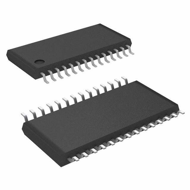
ICGOO电子元器件商城为您提供ADS8505IBDW由Texas Instruments设计生产,在icgoo商城现货销售,并且可以通过原厂、代理商等渠道进行代购。 ADS8505IBDW价格参考¥111.42-¥185.81。Texas InstrumentsADS8505IBDW封装/规格:数据采集 - 模数转换器, 16 Bit Analog to Digital Converter 1 Input 1 SAR 28-SOIC。您可以下载ADS8505IBDW参考资料、Datasheet数据手册功能说明书,资料中有ADS8505IBDW 详细功能的应用电路图电压和使用方法及教程。
| 参数 | 数值 |
| 产品目录 | 集成电路 (IC)半导体 |
| 描述 | IC ADC 16BIT 250KSPS 28-SOIC模数转换器 - ADC 16-Bit 250kHz CMOS w/Parallel Interface |
| 产品分类 | |
| 品牌 | Texas Instruments |
| 产品手册 | http://www.ti.com/litv/slas180b |
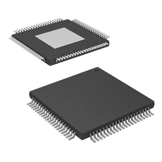
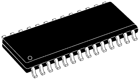
| 产品图片 |
|
| rohs | 符合RoHS无铅 / 符合限制有害物质指令(RoHS)规范要求 |
| 产品系列 | 数据转换器IC,模数转换器 - ADC,Texas Instruments ADS8505IBDW- |
| 数据手册 | |
| 产品型号 | ADS8505IBDW |
| 产品培训模块 | http://www.digikey.cn/PTM/IndividualPTM.page?site=cn&lang=zhs&ptm=13240 |
| 产品目录页面 | |
| 产品种类 | 模数转换器 - ADC |
| 位数 | 16 |
| 供应商器件封装 | 28-SOIC |
| 信噪比 | 88 dB |
| 其它名称 | 296-18676-5 |
| 分辨率 | 16 bit |
| 制造商产品页 | http://www.ti.com/general/docs/suppproductinfo.tsp?distId=10&orderablePartNumber=ADS8505IBDW |
| 包装 | 管件 |
| 单位重量 | 730.800 mg |
| 商标 | Texas Instruments |
| 安装类型 | 表面贴装 |
| 安装风格 | SMD/SMT |
| 封装 | Tube |
| 封装/外壳 | 28-SOIC(0.295",7.50mm 宽) |
| 封装/箱体 | SOIC-28 |
| 工作温度 | -40°C ~ 85°C |
| 工作电源电压 | 5 V |
| 工厂包装数量 | 20 |
| 接口类型 | Parallel |
| 数据接口 | 并联 |
| 最大功率耗散 | 100 mW |
| 最大工作温度 | + 85 C |
| 最小工作温度 | - 40 C |
| 标准包装 | 20 |
| 特性 | - |
| 电压参考 | Internal, External |
| 电压源 | 模拟和数字 |
| 系列 | ADS8505 |
| 结构 | SAR |
| 转换器数 | 1 |
| 转换器数量 | 1 |
| 转换速率 | 250 kS/s |
| 输入数和类型 | 1 个单端,双极 |
| 输入类型 | Single-Ended |
| 通道数量 | 1 Channel |
| 配用 | /product-detail/zh/ADS8505EVM/296-20817-ND/1216422 |
| 采样率(每秒) | 250k |






- 商务部:美国ITC正式对集成电路等产品启动337调查
- 曝三星4nm工艺存在良率问题 高通将骁龙8 Gen1或转产台积电
- 太阳诱电将投资9.5亿元在常州建新厂生产MLCC 预计2023年完工
- 英特尔发布欧洲新工厂建设计划 深化IDM 2.0 战略
- 台积电先进制程称霸业界 有大客户加持明年业绩稳了
- 达到5530亿美元!SIA预计今年全球半导体销售额将创下新高
- 英特尔拟将自动驾驶子公司Mobileye上市 估值或超500亿美元
- 三星加码芯片和SET,合并消费电子和移动部门,撤换高东真等 CEO
- 三星电子宣布重大人事变动 还合并消费电子和移动部门
- 海关总署:前11个月进口集成电路产品价值2.52万亿元 增长14.8%




PDF Datasheet 数据手册内容提取
(cid:2)(cid:17)(cid:14)(cid:14)(cid:20)(cid:2)(cid:14)(cid:13)(cid:18)(cid:12) (cid:4)(cid:14)(cid:13)(cid:8)(cid:17)(cid:7)(cid:16)(cid:15) (cid:10)(cid:14)(cid:13)(cid:11) (cid:5)(cid:9)(cid:19)(cid:6)(cid:15) (cid:3)(cid:12)(cid:15)(cid:16)(cid:14)(cid:17)(cid:11)(cid:9)(cid:12)(cid:16)(cid:15) ADS8505 SLAS180B–SEPTEMBER2005–REVISEDJUNE2007 16-BIT 250-KSPS SAMPLING CMOS ANALOG-TO-DIGITAL CONVERTER FEATURES APPLICATIONS • 105dBSFDRat250-kHzSampleRate • IndustrialProcessControl • Standard– 10-VInputRange • DataAcquisitionSystems • – 1.5LSBMaxINL • DigitalSignalProcessing • – 1LSBMaxDNL,16-BitsNoMissingCodes • MedicalEquipment • – 2mVMaxBipolarZeroErrorWith– 0.4 • Instrumentation PPM/(cid:176) CDrift DESCRIPTION • – 0.1%FSRMaxFull-ScaleErrorWith– 2 PPM/(cid:176) CDrift The ADS8505 is a complete 16-bit sampling A/D converter using state-of-the-art CMOS structures. It • Single5-VSupplyOperation contains a complete 16-bit, capacitor-based, SAR • Pin-CompatibleWithADS7805(LowSpeed) A/D with S/H, reference, clock, interface for and12-BitADS8504/7804 microprocessoruse,and3-stateoutputdrivers. • UsesInternalorExternalReference The ADS8505 is specified at a 250-kHz sampling • FullParallelDataOutput rate over the full temperature range. Precision • 70-mWTypPowerDissipationat250KSPS resistors provide an industry standard – 10-V input range, while the innovative design allows operation • 28-PinSSOPandSOICPackages from a single +5-V supply, with power dissipation under100mW. The ADS8505 is available in 28-pin SOIC and 28-pin SSOP packages, both fully specified for operation overtheindustrial–40(cid:176) Cto85(cid:176) Ctemperaturerange. R/C Clock Successive Approximation Register and Control Logic CS BYTE BUSY CDAC Output 9.8 kΩ Latches Three ±10 V Input and State Three Parallel 5 kΩ 2 kΩ State Data Comparator Drivers Bus CAP Buffer Internal +2.5 V Ref 4 kΩ REF Pleasebeawarethatanimportantnoticeconcerningavailability,standardwarranty,anduseincriticalapplicationsofTexas Instrumentssemiconductorproductsanddisclaimerstheretoappearsattheendofthisdatasheet. PRODUCTIONDATAinformationiscurrentasofpublicationdate. Copyright©2005–2007,TexasInstrumentsIncorporated Products conform to specifications per the terms of the Texas Instruments standard warranty. Production processing does not necessarilyincludetestingofallparameters.
ADS8505 www.ti.com SLAS180B–SEPTEMBER2005–REVISEDJUNE2007 Thesedeviceshavelimitedbuilt-inESDprotection.Theleadsshouldbeshortedtogetherorthedeviceplacedinconductivefoam duringstorageorhandlingtopreventelectrostaticdamagetotheMOSgates. PACKAGE/ORDERINGINFORMATION(1) MINIMUM NO MINIMUM SPECIFICATION RELATIVE PACKAGE PACKAGE ORDERING TRANSPORT PRODUCT MISSING SINAD TEMPERATURE ACCURACY LEAD DESIGNATOR NUMBER MEDIA,QTY CODE (dB) RANGE (LSB) ADS8505IBDW Tube,20 SO-28 DW ADS8505IBDWR TapeandReel,1000 ADS8505IB –1.5 16 86 –40(cid:176)C to85(cid:176)C ADS8505IBDB Tube,50 SSOP-28 DB ADS8505IBDBR TapeandReel,2000 ADS8505IDW Tube,20 SO-28 DW ADS8505IDWR TapeandReel,1000 ADS8505I – 4 15 83 –40(cid:176)Cto85(cid:176)C ADS8505IDB Tube,50 SSOP-28 DB ADS8505IDBR TapeandReel,2000 (1) Forthemostcurrentpackageandorderinginformation,seethePackageOptionAddendumattheendofthisdocument,orseetheTI websiteatwww.ti.com. ABSOLUTE MAXIMUM RATINGS(1) overoperatingfree-airtemperaturerange(unlessotherwisenoted)(2) UNIT V – 25V IN Analoginputs REF +V +0.3VtoAGND2–0.3V ANA CAP IndefiniteshorttoAGND2,momentaryshorttoV ANA DGND,AGND1,AGND2 – 0.3V V 6V ANA Groundvoltagedifferences V toV 0.3V DIG ANA V 6V DIG Digitalinputs –0.3Vto+V +0.3V DIG Maximumjunctiontemperature 165(cid:176) C Internalpowerdissipation 825mW Leadtemperature(soldering,10s) 300(cid:176) C (1) Stressesbeyondthoselistedunder"absolutemaximumratings"maycausepermanentdamagetothedevice.Thesearestressratings only,andfunctionaloperationofthedeviceattheseoranyotherconditionsbeyondthoseindicatedunder"recommendedoperating conditions"isnotimplied.Exposuretoabsolute-maximum-ratedconditionsforextendedperiodsmayaffectdevicereliability. (2) Allvoltagevaluesarewithrespecttonetworkgroundterminal. ELECTRICAL CHARACTERISTICS T =–40(cid:176) Cto85(cid:176) C,f =250kHz,V =V =5V,usinginternalreference(unlessotherwisenoted) A s DIG ANA ADS8505I ADS8505IB PARAMETER TESTCONDITIONS UNIT MIN TYP MAX MIN TYP MAX Resolution 16 16 Bits ANALOGINPUT Voltagerange – 10 – 10 V Impedance 11.5 11.5 kW Capacitance 50 50 pF THROUGHPUTSPEED Conversioncycle Acquireandconvert 4 4 m s Throughputrate 250 250 kHz 2 SubmitDocumentationFeedback
ADS8505 www.ti.com SLAS180B–SEPTEMBER2005–REVISEDJUNE2007 ELECTRICAL CHARACTERISTICS (continued) T =–40(cid:176) Cto85(cid:176) C,f =250kHz,V =V =5V,usinginternalreference(unlessotherwisenoted) A s DIG ANA ADS8505I ADS8505IB PARAMETER TESTCONDITIONS UNIT MIN TYP MAX MIN TYP MAX DCACCURACY INL Integrallinearityerror –4 4 –1.5 1.5 LSB(1) DNL Differentialllinearityerror –2 2 –1 1 LSB(1) Nomissingcodes 15 16 Bits Transitionnoise(2) 0.77 0.77 LSB Full-scaleerror(3)(4) Int.ref. –0.5 0.5 –0.25 0.25 %FSR Full-scaleerrordrift Int.ref. – 7 – 7 ppm/(cid:176)C Full-scaleerror(3)(4) Ext.2.5-Vref. –0.25 0.25 –0.1 – 0.01 0.1 %FSR Full-scaleerrordrift Ext.2.5-Vref. – 2 – 2 ppm/(cid:176)C Bipolarzeroerror(3) –5 5 –2 2 mV Bipolarzeroerrordrift – 0.4 – 0.4 ppm/(cid:176)C Powersupplysensitivity –8 8 –8 8 (VDIG=VANA=VD) +4.75V<VD<+5.25V LSB ACACCURACY SFDR Spuriousfreedynamicrange fI=20kHz 92 98 96 105 dB(5) THD Totalharmonicdistortion fI=20kHz –98 –92 –103 –96 dB fI=20kHz 83 88 86 88 dB SINAD Signal-to-(noise+distortion) –60-dBInput 30 32 dB SNR Signal-to-noiseratio fI=20kHz 83 88 86 88 dB Full-powerbandwidth(6) 500 500 kHz SAMPLINGDYNAMICS Aperturedelay 5 5 ns Transientresponse FSStep 2 2 m s Overvoltagerecovery(7) 150 150 ns REFERENCE Internalreferencevoltage 2.48 2.5 2.52 2.48 2.5 2.52 V Internalreferencesourcecurrent(must 1 1 m A useexternalbuffer) Internalreferencedrift 8 8 ppm/(cid:176)C Externalreferencevoltagerangefor 2.3 2.5 2.7 2.3 2.5 2.7 V specifiedlinearity Externalreferencecurrentdrain Ext.2.5-Vref. 100 100 m A DIGITALINPUTS Logiclevels VIL Low-levelinputvoltage –0.3 0.8 –0.3 0.8 V VIH High-levelinputvoltage 2.0 VDIG+0.3V 2.0 VDIG+0.3V V IIL Low-levelinputcurrent – 10 – 10 m A IIH High-levelinputcurrent – 10 – 10 m A DIGITALOUTPUTS Dataformat(parallel16-bits) Datacoding(binary2'scomplement) VOL Low-leveloutputvoltage ISINK=1.6mA 0.4 0.4 V VOH High-leveloutputvoltage ISOURCE=500mA 4 4 V Leakagecurrent Hi-Zstate, – 5 – 5 m A VOUT=0VtoVDIG Outputcapacitance Hi-Zstate 15 15 pF (1) LSBmeansleastsignificantbit.Forthe16-bit,– 10-VinputADS8505,oneLSBis305m V. (2) Typicalrmsnoiseatworstcasetransitionsandtemperatures. (3) AsmeasuredwithfixedresistorsshowninFigure27.Adjustabletozerowithexternalpotentiometer. (4) Full-scaleerroristheworstcaseof–full-scaleor+full-scaledeviationfromidealfirstandlastcodetransitions,dividedbythetransition voltage(notdividedbythefull-scalerange)andincludestheeffectofoffseterror. (5) AllspecificationsindBarereferredtoafull-scale– 10-Vinput. (6) Full-powerbandwidthisdefinedasthefull-scaleinputfrequencyatwhichsignal-to-(noise+distortion)degradesto60dB,or10bitsof accuracy. (7) Recoverstospecifiedperformanceafter2xFSinputovervoltage. SubmitDocumentationFeedback 3
ADS8505 www.ti.com SLAS180B–SEPTEMBER2005–REVISEDJUNE2007 ELECTRICAL CHARACTERISTICS (continued) T =–40(cid:176) Cto85(cid:176) C,f =250kHz,V =V =5V,usinginternalreference(unlessotherwisenoted) A s DIG ANA ADS8505I ADS8505IB PARAMETER TESTCONDITIONS UNIT MIN TYP MAX MIN TYP MAX DIGITALTIMING Busaccesstiming 83 83 ns Busrelinquishtiming 83 83 ns POWERSUPPLIES VDIG Digitalinputvoltage 4.75 5 5.25 4.75 5 5.25 V VANA Analoginputvoltage Mustbe£ VANA 4.75 5 5.25 4.75 5 5.25 V IDIG Digitalinputcurrent 2 5 2 5 mA IANA Analoginputcurrent 12 15 12 15 mA Powerdissipation fS=250kHz 70 100 70 100 mW TEMPERATURERANGE Specifiedperformance –40 85 –40 85 (cid:176)C Deratedperformance(8) –55 125 –55 125 (cid:176)C Storage –65 150 –65 150 (cid:176)C THERMALRESISTANCE(Q JA) SSOP 62 62 (cid:176)C/W SO 46 46 (cid:176)C/W (8) Theinternalreferencemaynotbestartedcorrectlybeyondtheindustrialtemperaturerange(–40(cid:176) Cto85(cid:176) C),thereforeuseofan externalreferenceisrecommended. DEVICE INFORMATION DBORDWPACKAGE (TOPVIEW) VIN 1 28 VDIG AGND1 2 27 VANA REF 3 26 BUSY CAP 4 25 CS AGND2 5 24 R/C D15 (MSB) 6 23 BYTE D14 7 22 D0 (LSB) D13 8 21 D1 D12 9 20 D2 D11 10 19 D3 D10 11 18 D4 D9 12 17 D5 D8 13 16 D6 DGND 14 15 D7 4 SubmitDocumentationFeedback
ADS8505 www.ti.com SLAS180B–SEPTEMBER2005–REVISEDJUNE2007 DEVICE INFORMATION (continued) TerminalFunctions TERMINAL DIGITAL DESCRIPTION NAME DB/DWNO. I/O AGND1 2 Analogground.Usedinternallyasgroundreferencepoint. AGND2 5 Analogground. BUSY 26 O Atthestartofaconversion,BUSYgoeslowandstayslowuntiltheconversionis completedandthedigitaloutputshavebeenupdated. BYTE 23 I Selects8mostsignificantbits(low)or8leastsignificantbits(high). CAP 4 Referencebuffercapacitor.2.2-m FTantalumcapacitortoground. CS 25 I InternallyORedwithR/C.IfR/Cislow,afallingedgeonCSinitiatesanewconversion. DGND 14 Digitalground. D15(MSB) 6 O Databit15.Mostsignificantbit(MSB)ofconversionresults.Hi-ZstatewhenCSis high,orwhenR/Cislow. D14 7 O Databit14.Hi-ZstatewhenCSishigh,orwhenR/Cislow. D13 8 O Databit13.Hi-ZstatewhenCSishigh,orwhenR/Cislow. D12 9 O Databit12.Hi-ZstatewhenCSishigh,orwhenR/Cislow. D11 10 O Databit11.Hi-ZstatewhenCSishigh,orwhenR/Cislow. D10 11 O Databit10.Hi-ZstatewhenCSishigh,orwhenR/Cislow. D9 12 O Databit9.Hi-ZstatewhenCSishigh,orwhenR/Cislow. D8 13 O Databit8.Hi-ZstatewhenCSishigh,orwhenR/Cislow. D7 15 O Databit7.Hi-ZstatewhenCSishigh,orwhenR/Cislow. D6 16 O Databit6.Hi-ZstatewhenCSishigh,orwhenR/Cislow. D5 17 O Databit5.Hi-ZstatewhenCSishigh,orwhenR/Cislow. D4 18 O Databit4.Hi-ZstatewhenCSishigh,orwhenR/Cislow. D3 19 O Databit3.Hi-ZstatewhenCSishigh,orwhenR/Cislow. D2 20 O Databit2.Hi-ZstatewhenCSishigh,orwhenR/Cislow. D1 21 O Databit1.Hi-ZstatewhenCSishigh,orwhenR/Cislow. D0(LSB) 22 O Databit0.Leastsignificantbit(LSB)ofconversionresults.Hi-ZstatewhenCSishigh, orwhenR/Cislow. R/C 24 I WithCSlowandBUSYhigh,afallingedgeonR/Cinitiatesanewconversion.WithCS low,arisingedgeonR/Cenablestheparalleloutput. REF 3 Referenceinput/output.2.2-m FTantalumcapacitortoground. V 27 Analogsupplyinput.Nominally+5V.Decoupletogroundwith0.1-m Fceramicand ANA 10-m Ftantalumcapacitors. V 28 Digitalsupplyinput.Nominally+5V.Connectdirectlytopin27.Mustbe£ V . DIG ANA V 1 Analoginput.SeeFigure28. IN SubmitDocumentationFeedback 5
ADS8505 www.ti.com SLAS180B–SEPTEMBER2005–REVISEDJUNE2007 TYPICAL CHARACTERISTICS SPURIOUSFREEDYNAMICRANGE TOTALHARMONICDISTORTION SIGNAL-TO-NOISERATIO vs vs vs FREE-AIRTEMPERATURE FREE-AIRTEMPERATURE FREE-AIRTEMPERATURE B 110 -105 100 d DR - Spurious Free Dynamic Range - 119089005550 ffsi== 2205 0kH KzSPS, THotaD - Tl Harmonic Distortion - dB -1----0998805050 ffsi== 2205 0k HKzSPS SNR - Signal-to-Noise Ratio - dB 7889950505 ffsi== 2205 0k HKzSPS SF 80 -75 70 -40 -20 0 20 40 60 80 -40 -20 0 20 40 60 80 -40 -20 0 20 40 60 80 TA- Free-Air Temperature -ºC TA- Free-Air Temperature -ºC TA- Free-Air Temperature -ºC Figure1. Figure2. Figure3. SIGNAL-TO-NOISE SIGNAL-TO-NOISE ANDDISTORTION SIGNAL-TO-NOISERATIO ANDDISTORTION vs vs vs FREE-AIRTEMPERATURE INPUTFREQUENCY INPUTFREQUENCY AD - Signal-to-Noise and Distortion - dB 1897890505050 ffsI== 2205 0kH KzSPS SNR - Signal-to-Noise Ratio - dB 1089798055500 AD - Signal-to-Noise and Distortion - dB 11006778899055050505 SIN 70 70 SIN 60 -40 -20 0 20 40 60 80 1 10 100 125 1 10 100 125 TA- Free-Air Temperature -ºC fi- Input Frequency - kHz fi- Input Frequency - kHz Figure4. Figure5. Figure6. SPURIOUSFREEDYNAMICRANGE TOTALHARMONICDISTORTION INTERNALREFERENCEVOLTAGE vs vs vs INPUTFREQUENCY INPUTFREQUENCY FREE-AIRTEMPERATURE 120 120 2.510 B R - Spurious Free Dynamic Range - d 11110089189150555000 HD - Total Harmonic Distortion - dB 117890100000 Internal Reference Voltage − V 222222222.........444455555999900000246802468 D T SF 75 60 2.490 1 10 100125 1 10 100125 −40 −20 0 20 40 60 80 fi- Input Frequency - kHz fi- Input Frequency - kHz TA − Free-Air Temperature − (cid:1)C Figure7. Figure8. Figure9. 6 SubmitDocumentationFeedback
ADS8505 www.ti.com SLAS180B–SEPTEMBER2005–REVISEDJUNE2007 TYPICAL CHARACTERISTICS (continued) BIPOLARZEROSCALEERROR NEGATIVEFULL-SCALEERROR NEGATIVEFULL-SCALEERROR vs vs vs FREE-AIRTEMPERATURE FREE-AIRTEMPERATURE FREE-AIRTEMPERATURE 5 0.25 0.2 mV 4 R 0.2 Internal Reference R 0.15 External Reference BPZ − Bipolar Zero Scale Error − −−−−01234321 Negative Full−Scale Error − %FS −−−−0000..0..000110...55105521 Negative Full−Scale Error − %FS −−−000.0..0010..510551 −5 −0.25 −0.2 −40 −20 0 20 40 60 80 −40 −20 0 20 40 60 80 −40 −20 0 20 40 60 80 TA − Free-Air Temperature − (cid:1)C TA − Free-Air Temperature − (cid:1)C TA − Free-Air Temperature − (cid:1)C Figure10. Figure11. Figure12. POSITIVEFULL-SCALEERROR POSITIVEFULL-SCALEERROR SUPPLYCURRENT vs vs vs FREE-AIRTEMPERATURE FREE-AIRTEMPERATURE FREE-AIRTEMPERATURE 0.25 0.2 20 0.2 Internal Reference External Reference 19 Positive Full−Scale Error − %FSR −−−−0000..0..000110...55105521 Positive Full−Scale Error − %FSR−−−0000..0..00110..5510551 I- Supply Current - mADD 1111111123456781 −0.25 −0.2 10 −40 −20 0 20 40 60 80 −40 −20 0 20 40 60 80 -40 -20 0 20 40 60 80 TA − Free-Air Temperature − (cid:1)C TA − Free-Air Temperature − (cid:1)C TA- Free-Air Temperature -ºC Figure13. Figure14. Figure15. PERFORMANCE vs HISTOGRAM CAPPINCAPACITORESR 4500 110 4000 8C1o9n2versions 4028 |THD | of a DC Input 100 3500 3000 SINAD e 90 c Hits2500 2221 man 80 2000 1713 erfor 1500 P 70 1000 60 2.2mF Capacitor on 500 CAPPin (pin 4) 1 151 76 2 0 50 −3 −2 −1 0 1 2 3 0 1 2 3 4 5 6 7 8 9 10 Code ESR - Resistance -W Figure16. Figure17. SubmitDocumentationFeedback 7
ADS8505 www.ti.com SLAS180B–SEPTEMBER2005–REVISEDJUNE2007 TYPICAL CHARACTERISTICS (continued) INTEGRALNONLINEARITY 1.5 1 0.5 s B S L 0 - L N I -0.5 -1 -1.5 0 16384 32768 49152 65536 Code Figure18. DIFFERENTIALNONLINEARITY 1 0.5 s B S L 0 - L N D -0.5 -1 0 16384 32768 49152 65536 Code Figure19. FFT(20-kHzInput) 20 0 8192 Points -20 fs= 250 KSPS B fi= 20 KHz, 0dB d -40 SINAD = 87.7 dB e - -60 THD = -103.9 dB d u -80 plit -100 m A -120 -140 -160 -180 0 25 50 75 100 125 f - Frequency - kHz Figure20. BASIC OPERATION Figure 21 shows a basic circuit to operate the ADS8505 with a full parallel data output. Taking R/C (pin 24) low for a minimum of 40 ns (1.75 m s max) initiates a conversion. BUSY (pin 26) goes low and stays low until the conversion is completed and the output registers are updated. Data is output in binary 2's complement format withtheMSBonpin6.BUSYgoinghighcanbeusedtolatchthedata. 8 SubmitDocumentationFeedback
ADS8505 www.ti.com SLAS180B–SEPTEMBER2005–REVISEDJUNE2007 BASIC OPERATION (continued) The ADS8505 begins tracking the input signal at the end of the conversion. Allowing 4 m s between convert commandsassuresaccurateacquisitionofanewsignal. The offset and gain are adjusted internally to allow external trimming with a single supply. The external resistors compensate for this adjustment and can be left out if the offset and gain are corrected in software (refer to the CALIBRATIONsection). STARTINGACONVERSION The combination of CS (pin 25) and R/C (pin 24) low for a minimum of 40 ns immediately puts the sample/hold of the ADS8505 in the hold state and starts conversion n. BUSY (pin 26) goes low and stays low until conversion n is completed and the internal output register has been updated. All new convert commands during BUSYlowwillaborttheconversioninprogressandresettheADC(seeFigure26). The ADS8505 begins tracking the input signal at the end of the conversion. Allowing 4 m s between convert commands assures accurate acquisition of a new signal. Refer to Table 1 for a summary of CS, R/C, and BUSY statesandFigure23throughFigure25forthetimingdiagrams. CS and R/C are internally ORed and level triggered. There is not a requirement which input goes low first when initiating a conversion. If, however, it is critical that CS or R/C initiates conversion n, be sure the less critical inputislowatleast10nspriortotheinitiatinginput. To reduce the number of control pins, CS can be tied low using R/C to control the read and convert modes. The paralleloutputbecomesactivewheneverR/Cgoeshigh.RefertotheREADINGDATAsection. Table1.ControlLineFunctionsforReadandConvert CS R/C BUSY OPERATION 1 X X None.DatabusisinHi-Zstate. fl 0 1 Initiatesconversionn.DatabusremainsinHi-Zstate. 0 fl 1 Initiatesconversionn.DatabusentersHi-Zstate. 0 1 › Conversionncompleted.Validdatafromconversionnonthedatabus. fl 1 1 Enablesdatabuswithvaliddatafromconversionn. fl 1 0 Enablesdatabuswithvaliddatafromconversionn-1(1).Conversionninprogress. 0 › 0 Enablesdatabuswithvaliddatafromconversionn-1(1).Conversionninprogress. 0 0 › Dataisinvalid.CSand/orR/CmustbehighwhenBUSYgoeshigh. X fl 0 Conversionnishalted.CausesADCtoreset.(2) (1) SeeFigure23andFigure24forconstraintsondatavalidfromconversionn-1. (2) SeeFigure26fordetailsonADCreset. SubmitDocumentationFeedback 9
ADS8505 www.ti.com SLAS180B–SEPTEMBER2005–REVISEDJUNE2007 200 W 1 28 33.2 kW 2.2 m F 2 27 +0.1 m F +10 m F+5V + 3 26 4 25 2.2 m F + Convert Pulse 5 24 B15 (MSB) 6 23 B14 7 22 B0 (LSB) 40 ns Min ADS8505 B13 8 21 B1 B12 9 20 B2 B11 10 19 B3 B10 11 18 B4 B9 12 17 B5 B8 13 16 B6 14 15 B7 Figure21.BasicOperation READING DATA The ADS8505 outputs full or byte-reading parallel data in binary 2's complement data output format. The parallel output is active when R/C (pin 24) is high and CS (pin 25) is low. Any other combination of CS and R/C 3-states the parallel output. Valid conversion data can be read in a full parallel, 16-bit word or two 8-bit bytes on pins 6-13 and pins 15-22. BYTE (pin 23) can be toggled to read both bytes within one conversion cycle. Refer to Table2foridealoutputcodesandFigure22forbitlocationsrelativetothestateofBYTE. Table2.IdealInputVoltagesandOutputCodes DIGITALOUTPUTBINARY2'SCOMPLEMENT DESCRIPTION ANALOGINPUT BINARYCODE HEXCODE Full-scalerange – 10V Leastsignificantbit(LSB) 305m V Fullscale(10V-1LSB) 9.999695V 0111111111111111 7FFF Midscale 0V 0000000000000000 0000 OneLSBbelowmidscale -305m V 1111111111111111 FFFF –Fullscale -10V 1000000000000000 8000 PARALLEL OUTPUT (After a Conversion) After conversion n is completed and the output registers have been updated, BUSY (pin 26) goes high. Valid data from conversion n is available on D15-D0 (pins 6-13 and 15-22). BUSY going high can be used to latch the data.RefertoTable3,Figure23,Figure24,andFigure25fortimingspecifications. PARALLEL OUTPUT (During a Conversion) After conversion n has been initiated, valid data from conversion n-1 can be read and is valid up to t (2.2 m s 2 typ) after the start of conversion n. Do not attempt to read data from t (2.2 m s typ) after the start of conversion n 2 untilBUSY(pin26)goeshigh;thismayresultinreadinginvaliddata.RefertoTable3,Figure 23, Figure 24, and Figure25fortimingspecifications. Note: For the best possible performance, data should not be read during a conversion. The switching noise of theasynchronousdatatransfercancausedigitalfeedthroughdegradingconverterperformance. 10 SubmitDocumentationFeedback
ADS8505 www.ti.com SLAS180B–SEPTEMBER2005–REVISEDJUNE2007 The number of control lines can be reduced by tying CS low while using the falling edge of R/C to initiate conversionsandtherisingedgeofR/Ctoactivatetheoutputmodeoftheconverter.SeeFigure23. Table3.ConversionTiming SYMBOL DESCRIPTION MIN TYP MAX UNITS t Pulseduration,convert 40 1750 ns w1 t Accesstime,datavalidafterR/Clow 2.2 3.2 m s a t Propagationdelaytime,BUSYfromR/Clow 15 25 ns pd t Pulseduration,BUSYlow 2.2 m s w2 t Delaytime,BUSYafterendofconversion 5 ns d1 t Delaytime,aperture 5 ns d2 t Conversiontime 2.2 m s conv t Acquisitiontime 1.8 m s acq t Disabletime,bus 10 30 83 ns dis t Delaytime,BUSYafterdatavalid 35 50 ns d3 t Validtime,previousdataremainsvalidafterR/Clow 1.5 2 m s v t +t Throughputtime 4 m s conv acq t Setuptime,R/CtoCS 10 ns su t Cycletimebetweenconversions 4 m s c t Enabletime,bus 10 30 83 ns en t Delaytime,BYTE 5 10 30 ns d4 BYTE LOW BYTE HIGH +5 V Bit 15 (MSB) 6 23 Bit 7 6 23 Bit 14 7 22 Bit 0 (LSB) Bit 6 7 22 Bit 8 ADS8505 ADS8505 Bit 13 8 21 Bit 1 Bit 5 8 21 Bit 9 Bit 12 9 20 Bit 2 Bit 4 9 20 Bit 10 Bit 11 10 19 Bit 3 Bit 3 10 19 Bit 11 Bit 10 11 18 Bit 4 Bit 2 11 18 Bit 12 Bit 9 12 17 Bit 5 Bit 1 12 17 Bit 13 Bit 8 13 16 Bit 6 Bit 0 (LSB) 13 16 Bit 14 14 15 Bit 7 14 15 Bit 15 (MSB) Figure22. BitLocationsRelativetoStateofBYTE(Pin23) SubmitDocumentationFeedback 11
ADS8505 www.ti.com SLAS180B–SEPTEMBER2005–REVISEDJUNE2007 tw1 R/C tc ta1 tw2 BUSY tpd td2 td1 MODE Acquire Convert Acquire Convert tconv tacq Previous Previous DATA BUS Hi−Z Not Valid Data Valid Hi−Z Data Valid Data Valid Data Valid tdis td3 tv Figure23.ConversionTimingwithOutputsEnabledafterConversion(CSTiedLow) tsu tsu tsu tsu R/C tw1 CS tpd tw2 BUSY td2 MODE Acquire Convert Acquire tconv DATA BUS Hi−Z State Data Valid Hi−Z State ten tdis Figure24. UsingCStoControlConversionandReadTiming tsu tsu R/C CS BYTE Pins 6 − 13 Hi−Z High Byte Low Byte Hi−Z ten td4 tdis Pins 15 − 22 Hi−Z Low Byte High Byte Hi−Z Figure25.UsingCSandBYTEtoControlDataBus 12 SubmitDocumentationFeedback
ADS8505 www.ti.com SLAS180B–SEPTEMBER2005–REVISEDJUNE2007 t c t t w1 w1 R/C tpd tpd BUSY 0 ns MIN 4.75V VANA VDIG DATABUS Unknown Hi-Z Not Valid Hi-Z Not Valid Data Valid t d3 Figure26.ADCReset ADC RESET TheADCresetfunctionoftheADS8505canbeusedtoterminatethecurrentconversioncycle.BringingR/Clow for at least 40 ns while BUSY is low will initiate the ADC reset. To initiate a new conversion, R/C must return to thehighstateandremainhighlongenoughtoacquireanewsample(see Table 3, t ) before going low to initiate c the next conversion sequence. In applications that do not monitor the BUSY signal, it is recommended that the ADCresetfunctionbeimplementedaspartofasysteminitializationsequence. INPUT RANGES The ADS8505 offers a standard – 10-V input range. Figure 28 shows the necessary circuit connections for the ADS8505 with and without hardware trim. Offset and full-scale error specifications are tested and specified with the fixed resistors shown in Figure 28(b). Full-scale error includes offset and gain errors measured at both +FS and–FS.AdjustmentsforoffsetandgainaredescribedintheCALIBRATIONsectionofthisdatasheet. Offset and gain are adjusted internally to allow external trimming with a single supply. The external resistors compensate for this adjustment and can be left out if the offset and gain are corrected in software (refer to the CALIBRATIONsection). The nominal input impedance of 11.5 kW results from the combination of the internal resistor network shown on the front page of the product data sheet and the external resistors. The input resistor divider network provides inherent overvoltage protection assured to at least – 25 V. The 1% resistors used for the external circuitry do not compromise the accuracy or drift of the converter. They have little influence relative to the internal resistors, and tightertolerancesarenotrequired. The input signal must be referenced to AGND1. This minimizes the ground loop problem typical to analog designs. The analog signal should be driven by a low impedance source. A typical driving circuit using an OPA627orOPA132isshowninFigure27. SubmitDocumentationFeedback 13
ADS8505 www.ti.com SLAS180B–SEPTEMBER2005–REVISEDJUNE2007 +15 V 2.2 (cid:2)F 22 pF ADS8505 200 (cid:1) 100 nF VIN GND 2 k(cid:1) Pin7 Pin1 2 k(cid:1) Vin Pin2 − REF OPA627 22 pF or 33.2 k(cid:1) 2.2 (cid:2)F OPA132 Pin6 + Pin3 AGND1 Pin4 GND CAP GND 2.2 (cid:2)F 2.2 (cid:2)F GND DGND 100 nF GND AGND2 −15V GND Figure27.TypicalDrivingCircuit(– 10V,NoTrim) 14 SubmitDocumentationFeedback
ADS8505 www.ti.com SLAS180B–SEPTEMBER2005–REVISEDJUNE2007 APPLICATION INFORMATION CALIBRATION The ADS8505 can be trimmed in hardware or software. The offset should be trimmed before the gain since the offsetdirectlyaffectsthegain.Toachieveoptimumperformance,severaliterationsmayberequired. Hardware Calibration To calibrate the offset and gain of the ADS8505, install the proper resistors and potentiometers as shown in Figure28(a). Software Calibration To calibrate the offset and gain of the ADS8505 in software, no external resistors are required. See the No Calibrationsectionfordetailsontheeffectsoftheexternalresistors. No Calibration See Figure 28(b) for circuit connections. The external resistors shown in Figure 28(b) may not be necessary in some applications. These resistors provide compensation for an internal adjustment of the offset and gain which allowscalibrationwithasinglesupply. ±10 V 200 W 1 VIN ±10 V 200 W 1 VIN 2 2 33.2 kW AGND1 AGND1 +5 V 2.2 m F+ 3 33.2 kW 2.2 m F+ 3 REF REF 50 kW 576 kW Offset 4 4 CAP CAP 50 kW Gain + + 2.2 m F 2.2 m F 5 5 AGND2 AGND2 (a) ±10 V With Hardware Trim (b) ±10 V Without Hardware Trim Note: Use 1% metal film resistors. Figure28.CircuitDiagramWithandWithoutExternalResistors REFERENCE The ADS8505 can operate with its internal 2.5-V reference or an external reference. By applying an external reference to pin 5, the internal reference can be bypassed. The reference voltage at REF is buffered internally withtheoutputonCAP(pin4). The internal reference has an 8 ppm/(cid:176) C drift (typical) and accounts for approximately 20% of the full-scale error (FSE=– 0.5%). REF REF(pin3)isaninputforanexternalreferenceor the output for the internal 2.5-V reference. A 2.2-m F capacitor shouldbeconnectedasclosetotheREFpinaspossible.Thecapacitorandtheoutputresistance of REF create a low-pass filter to bandlimit noise on the reference. Using a smaller value capacitor introduces more noise to thereferencedegradingtheSNRandSINAD.TheREFpinshouldnotbeusedtodriveexternalacordcloads. The range for the external reference is 2.3 V to 2.7 V and determines the actual LSB size. Increasing the referencevoltageincreasesthefull-scalerangeandtheLSBsizeoftheconverterwhichcanimprovetheSNR. SubmitDocumentationFeedback 15
ADS8505 www.ti.com SLAS180B–SEPTEMBER2005–REVISEDJUNE2007 APPLICATION INFORMATION (continued) CAP CAP (pin 4) is the output of the internal reference buffer. A 2.2-m F capacitor can be placed between the CAP pin and ground. Because the internal reference buffer is internally compensated, the external capacitor is not necessary for compensation of the reference buffer. This relaxes the performance requirements of the capacitor andmakestheperformanceoftheADClesssensitivetothecapacitor. The output of the buffer is capable of driving up to 2 mA of current to a dc load. A dc load requiring more than 2 mA of current from the CAP pin begins to degrade the linearity of the ADS8505. Using an external buffer allows the internal reference to be used for larger dc loads and ac loads. Do not attempt to directly drive an ac load withtheoutputvoltageonCAP.Thiscausesperformancedegradationoftheconverter. LAYOUT POWER For optimum performance, tie the analog and digital power pins to the same +5-V power supply and tie the analog and digital grounds together. As noted in the electrical specifications, the ADS8505 uses 90% of its powerfortheanalogcircuitry.TheADS8505shouldbeconsideredasananalogcomponent. The +5-V power for the A/D should be separate from the +5 V used for the system's digital logic. Connecting V (pin 28) directly to a digital supply can reduce converter performance due to switching noise from the digital DIG logic. For best performance, the +5-V supply can be produced from whatever analog supply is used for the rest of the analog signal conditioning. If +12-V or +15-V supplies are present, a simple +5-V regulator can be used. Although it is not suggested, if the digital supply must be used to power the converter, be sure to properly filter the supply. Either using a filtered digital supply or a regulated analog supply, both V and V should be tied DIG ANA tothesame+5-Vsource. GROUNDING Three ground pins are present on the ADS8505. DGND is the digital supply ground. AGND2 is the analog supplyground.AGND1isthegroundwhichallanalogsignalsinternaltotheA/Darereferenced.AGND1ismore susceptible to current induced voltage drops and must have the path of least resistance back to the power supply. All the ground pins of the A/D should be tied to the analog ground plane, separated from the system's digital logic ground, to achieve optimum performance. Both analog and digital ground planes should be tied to the system ground as near to the power supplies as possible. This helps to prevent dynamic digital ground currents frommodulatingtheanaloggroundthroughacommonimpedancetopowerground. SIGNAL CONDITIONING The FET switches used for the sample/hold on many CMOS A/D converters release a significant amount of charge injection which can cause the driving op-amp to oscillate. The FET switch on the ADS8505, compared to the FET switches on other CMOS A/D converters, releases 5% to 10% of the charge. There is also a resistive front end which attenuates any charge which is released. The end result is a minimal requirement for the anti-alias filter on the front end. Any op-amp sufficient for the signal in an application is sufficient to drive the ADS8505. The resistive front end of the ADS8505 also provides an assured – 25-V overvoltage protection. In most cases, thiseliminatestheneedforexternalinputprotectioncircuitry. INTERMEDIATE LATCHES The ADS8505 does have 3-state outputs for the parallel port, but intermediate latches should be used if the bus is to be active during conversions. If the bus is not active during conversion, the 3-state outputs can be used to isolate the A/D from other peripherals on the same bus. The 3-state outputs can also be used when the A/D is theonlyperipheralonthedatabus. 16 SubmitDocumentationFeedback
ADS8505 www.ti.com SLAS180B–SEPTEMBER2005–REVISEDJUNE2007 Intermediate latches are beneficial on any monolithic A/D converter. The ADS8505 has an internal LSB size of 38m V.Transientsfromfastswitchingsignalson the parallel port, even when the A/D is 3-stated, can be coupled throughthesubstratetotheanalogcircuitrycausingdegradationofconverterperformance. SubmitDocumentationFeedback 17
ADS8505 www.ti.com SLAS180B–SEPTEMBER2005–REVISEDJUNE2007 Revision History NOTE:Pagenumbersforpreviousrevisionsmaydifferfrompagenumbersinthecurrentversion. ChangesfromOriginal(September,2005)toARevision ............................................................................................. Page • AddedSFDRvalue............................................................................................................................................................... 1 • Changed3.0to1.5MaxINL................................................................................................................................................. 1 • Changed3.0to1.5MinimumRelativeAccuracy.................................................................................................................. 2 • ChangedREFandCAP-reversed...................................................................................................................................... 2 • ChangedINL,SFDR,THD,SNRvalues.............................................................................................................................. 2 • ChangedSFDR-TA,THD-TA,SINAD-TA,SNR-fi,SINAD-fiSFDR-fi,THD-fi,IDD-TA,CAPESR,INL,DNL,and FFTcurves............................................................................................................................................................................ 6 • ChangedCAPdescription................................................................................................................................................... 16 ChangesfromARevision(October,2006)toBRevision ............................................................................................. Page • Deletedtextfrombasicoperationdescription...................................................................................................................... 8 • Changedtextinstartingaconversiondescription................................................................................................................ 9 • ChangedoperationdescriptionsandR/Cintable................................................................................................................ 9 • AddedSARResettiming.................................................................................................................................................... 13 • AddedADCRESETsection............................................................................................................................................... 13 18 SubmitDocumentationFeedback
PACKAGE OPTION ADDENDUM www.ti.com 11-Jul-2017 PACKAGING INFORMATION Orderable Device Status Package Type Package Pins Package Eco Plan Lead/Ball Finish MSL Peak Temp Op Temp (°C) Device Marking Samples (1) Drawing Qty (2) (6) (3) (4/5) ADS8505IBDB ACTIVE SSOP DB 28 50 Green (RoHS CU NIPDAU Level-2-260C-1 YEAR -40 to 85 ADS8505I & no Sb/Br) B ADS8505IBDBG4 ACTIVE SSOP DB 28 50 Green (RoHS CU NIPDAU Level-2-260C-1 YEAR -40 to 85 ADS8505I & no Sb/Br) B ADS8505IBDBR ACTIVE SSOP DB 28 2000 Green (RoHS CU NIPDAU Level-2-260C-1 YEAR -40 to 85 ADS8505I & no Sb/Br) B ADS8505IBDBRG4 ACTIVE SSOP DB 28 2000 Green (RoHS CU NIPDAU Level-2-260C-1 YEAR -40 to 85 ADS8505I & no Sb/Br) B ADS8505IBDW ACTIVE SOIC DW 28 20 Green (RoHS CU NIPDAU Level-2-260C-1 YEAR -40 to 85 ADS8505I & no Sb/Br) B ADS8505IBDWG4 ACTIVE SOIC DW 28 20 Green (RoHS CU NIPDAU Level-2-260C-1 YEAR -40 to 85 ADS8505I & no Sb/Br) B ADS8505IBDWR ACTIVE SOIC DW 28 1000 Green (RoHS CU NIPDAU Level-2-260C-1 YEAR -40 to 85 ADS8505I & no Sb/Br) B ADS8505IDB ACTIVE SSOP DB 28 50 Green (RoHS CU NIPDAU Level-2-260C-1 YEAR -40 to 85 ADS8505I & no Sb/Br) ADS8505IDW ACTIVE SOIC DW 28 20 Green (RoHS CU NIPDAU Level-2-260C-1 YEAR -40 to 85 ADS8505I & no Sb/Br) ADS8505IDWG4 ACTIVE SOIC DW 28 20 Green (RoHS CU NIPDAU Level-2-260C-1 YEAR -40 to 85 ADS8505I & no Sb/Br) ADS8505IDWR ACTIVE SOIC DW 28 1000 Green (RoHS CU NIPDAU Level-2-260C-1 YEAR -40 to 85 ADS8505I & no Sb/Br) (1) The marketing status values are defined as follows: ACTIVE: Product device recommended for new designs. LIFEBUY: TI has announced that the device will be discontinued, and a lifetime-buy period is in effect. NRND: Not recommended for new designs. Device is in production to support existing customers, but TI does not recommend using this part in a new design. PREVIEW: Device has been announced but is not in production. Samples may or may not be available. OBSOLETE: TI has discontinued the production of the device. (2) RoHS: TI defines "RoHS" to mean semiconductor products that are compliant with the current EU RoHS requirements for all 10 RoHS substances, including the requirement that RoHS substance do not exceed 0.1% by weight in homogeneous materials. Where designed to be soldered at high temperatures, "RoHS" products are suitable for use in specified lead-free processes. TI may reference these types of products as "Pb-Free". RoHS Exempt: TI defines "RoHS Exempt" to mean products that contain lead but are compliant with EU RoHS pursuant to a specific EU RoHS exemption. Green: TI defines "Green" to mean the content of Chlorine (Cl) and Bromine (Br) based flame retardants meet JS709B low halogen requirements of <=1000ppm threshold. Antimony trioxide based flame retardants must also meet the <=1000ppm threshold requirement. Addendum-Page 1
PACKAGE OPTION ADDENDUM www.ti.com 11-Jul-2017 (3) MSL, Peak Temp. - The Moisture Sensitivity Level rating according to the JEDEC industry standard classifications, and peak solder temperature. (4) There may be additional marking, which relates to the logo, the lot trace code information, or the environmental category on the device. (5) Multiple Device Markings will be inside parentheses. Only one Device Marking contained in parentheses and separated by a "~" will appear on a device. If a line is indented then it is a continuation of the previous line and the two combined represent the entire Device Marking for that device. (6) Lead/Ball Finish - Orderable Devices may have multiple material finish options. Finish options are separated by a vertical ruled line. Lead/Ball Finish values may wrap to two lines if the finish value exceeds the maximum column width. Important Information and Disclaimer:The information provided on this page represents TI's knowledge and belief as of the date that it is provided. TI bases its knowledge and belief on information provided by third parties, and makes no representation or warranty as to the accuracy of such information. Efforts are underway to better integrate information from third parties. TI has taken and continues to take reasonable steps to provide representative and accurate information but may not have conducted destructive testing or chemical analysis on incoming materials and chemicals. TI and TI suppliers consider certain information to be proprietary, and thus CAS numbers and other limited information may not be available for release. In no event shall TI's liability arising out of such information exceed the total purchase price of the TI part(s) at issue in this document sold by TI to Customer on an annual basis. Addendum-Page 2
PACKAGE MATERIALS INFORMATION www.ti.com 11-Jul-2017 TAPE AND REEL INFORMATION *Alldimensionsarenominal Device Package Package Pins SPQ Reel Reel A0 B0 K0 P1 W Pin1 Type Drawing Diameter Width (mm) (mm) (mm) (mm) (mm) Quadrant (mm) W1(mm) ADS8505IBDBR SSOP DB 28 2000 330.0 16.4 8.1 10.4 2.5 12.0 16.0 Q1 ADS8505IBDWR SOIC DW 28 1000 330.0 32.4 11.35 18.67 3.1 16.0 32.0 Q1 ADS8505IDWR SOIC DW 28 1000 330.0 32.4 11.35 18.67 3.1 16.0 32.0 Q1 PackMaterials-Page1
PACKAGE MATERIALS INFORMATION www.ti.com 11-Jul-2017 *Alldimensionsarenominal Device PackageType PackageDrawing Pins SPQ Length(mm) Width(mm) Height(mm) ADS8505IBDBR SSOP DB 28 2000 367.0 367.0 38.0 ADS8505IBDWR SOIC DW 28 1000 367.0 367.0 55.0 ADS8505IDWR SOIC DW 28 1000 367.0 367.0 55.0 PackMaterials-Page2
None
None
MECHANICAL DATA MSSO002E – JANUARY 1995 – REVISED DECEMBER 2001 DB (R-PDSO-G**) PLASTIC SMALL-OUTLINE 28 PINS SHOWN 0,38 0,65 0,15 M 0,22 28 15 0,25 0,09 5,60 8,20 5,00 7,40 Gage Plane 1 14 0,25 A 0°–(cid:1)8° 0,95 0,55 Seating Plane 2,00 MAX 0,05 MIN 0,10 PINS ** 14 16 20 24 28 30 38 DIM A MAX 6,50 6,50 7,50 8,50 10,50 10,50 12,90 A MIN 5,90 5,90 6,90 7,90 9,90 9,90 12,30 4040065/E 12/01 NOTES: A. All linear dimensions are in millimeters. B. This drawing is subject to change without notice. C. Body dimensions do not include mold flash or protrusion not to exceed 0,15. D. Falls within JEDEC MO-150 • POST OFFICE BOX 655303 DALLAS, TEXAS 75265
IMPORTANTNOTICE TexasInstrumentsIncorporated(TI)reservestherighttomakecorrections,enhancements,improvementsandotherchangestoits semiconductorproductsandservicesperJESD46,latestissue,andtodiscontinueanyproductorserviceperJESD48,latestissue.Buyers shouldobtainthelatestrelevantinformationbeforeplacingordersandshouldverifythatsuchinformationiscurrentandcomplete. TI’spublishedtermsofsaleforsemiconductorproducts(http://www.ti.com/sc/docs/stdterms.htm)applytothesaleofpackagedintegrated circuitproductsthatTIhasqualifiedandreleasedtomarket.AdditionaltermsmayapplytotheuseorsaleofothertypesofTIproductsand services. ReproductionofsignificantportionsofTIinformationinTIdatasheetsispermissibleonlyifreproductioniswithoutalterationandis accompaniedbyallassociatedwarranties,conditions,limitations,andnotices.TIisnotresponsibleorliableforsuchreproduced documentation.Informationofthirdpartiesmaybesubjecttoadditionalrestrictions.ResaleofTIproductsorserviceswithstatements differentfromorbeyondtheparametersstatedbyTIforthatproductorservicevoidsallexpressandanyimpliedwarrantiesforthe associatedTIproductorserviceandisanunfairanddeceptivebusinesspractice.TIisnotresponsibleorliableforanysuchstatements. BuyersandotherswhoaredevelopingsystemsthatincorporateTIproducts(collectively,“Designers”)understandandagreethatDesigners remainresponsibleforusingtheirindependentanalysis,evaluationandjudgmentindesigningtheirapplicationsandthatDesignershave fullandexclusiveresponsibilitytoassurethesafetyofDesigners'applicationsandcomplianceoftheirapplications(andofallTIproducts usedinorforDesigners’applications)withallapplicableregulations,lawsandotherapplicablerequirements.Designerrepresentsthat,with respecttotheirapplications,Designerhasallthenecessaryexpertisetocreateandimplementsafeguardsthat(1)anticipatedangerous consequencesoffailures,(2)monitorfailuresandtheirconsequences,and(3)lessenthelikelihoodoffailuresthatmightcauseharmand takeappropriateactions.DesigneragreesthatpriortousingordistributinganyapplicationsthatincludeTIproducts,Designerwill thoroughlytestsuchapplicationsandthefunctionalityofsuchTIproductsasusedinsuchapplications. TI’sprovisionoftechnical,applicationorotherdesignadvice,qualitycharacterization,reliabilitydataorotherservicesorinformation, including,butnotlimitedto,referencedesignsandmaterialsrelatingtoevaluationmodules,(collectively,“TIResources”)areintendedto assistdesignerswhoaredevelopingapplicationsthatincorporateTIproducts;bydownloading,accessingorusingTIResourcesinany way,Designer(individuallyor,ifDesignerisactingonbehalfofacompany,Designer’scompany)agreestouseanyparticularTIResource solelyforthispurposeandsubjecttothetermsofthisNotice. TI’sprovisionofTIResourcesdoesnotexpandorotherwisealterTI’sapplicablepublishedwarrantiesorwarrantydisclaimersforTI products,andnoadditionalobligationsorliabilitiesarisefromTIprovidingsuchTIResources.TIreservestherighttomakecorrections, enhancements,improvementsandotherchangestoitsTIResources.TIhasnotconductedanytestingotherthanthatspecifically describedinthepublisheddocumentationforaparticularTIResource. Designerisauthorizedtouse,copyandmodifyanyindividualTIResourceonlyinconnectionwiththedevelopmentofapplicationsthat includetheTIproduct(s)identifiedinsuchTIResource.NOOTHERLICENSE,EXPRESSORIMPLIED,BYESTOPPELOROTHERWISE TOANYOTHERTIINTELLECTUALPROPERTYRIGHT,ANDNOLICENSETOANYTECHNOLOGYORINTELLECTUALPROPERTY RIGHTOFTIORANYTHIRDPARTYISGRANTEDHEREIN,includingbutnotlimitedtoanypatentright,copyright,maskworkright,or otherintellectualpropertyrightrelatingtoanycombination,machine,orprocessinwhichTIproductsorservicesareused.Information regardingorreferencingthird-partyproductsorservicesdoesnotconstitutealicensetousesuchproductsorservices,orawarrantyor endorsementthereof.UseofTIResourcesmayrequirealicensefromathirdpartyunderthepatentsorotherintellectualpropertyofthe thirdparty,oralicensefromTIunderthepatentsorotherintellectualpropertyofTI. TIRESOURCESAREPROVIDED“ASIS”ANDWITHALLFAULTS.TIDISCLAIMSALLOTHERWARRANTIESOR REPRESENTATIONS,EXPRESSORIMPLIED,REGARDINGRESOURCESORUSETHEREOF,INCLUDINGBUTNOTLIMITEDTO ACCURACYORCOMPLETENESS,TITLE,ANYEPIDEMICFAILUREWARRANTYANDANYIMPLIEDWARRANTIESOF MERCHANTABILITY,FITNESSFORAPARTICULARPURPOSE,ANDNON-INFRINGEMENTOFANYTHIRDPARTYINTELLECTUAL PROPERTYRIGHTS.TISHALLNOTBELIABLEFORANDSHALLNOTDEFENDORINDEMNIFYDESIGNERAGAINSTANYCLAIM, INCLUDINGBUTNOTLIMITEDTOANYINFRINGEMENTCLAIMTHATRELATESTOORISBASEDONANYCOMBINATIONOF PRODUCTSEVENIFDESCRIBEDINTIRESOURCESOROTHERWISE.INNOEVENTSHALLTIBELIABLEFORANYACTUAL, DIRECT,SPECIAL,COLLATERAL,INDIRECT,PUNITIVE,INCIDENTAL,CONSEQUENTIALOREXEMPLARYDAMAGESIN CONNECTIONWITHORARISINGOUTOFTIRESOURCESORUSETHEREOF,ANDREGARDLESSOFWHETHERTIHASBEEN ADVISEDOFTHEPOSSIBILITYOFSUCHDAMAGES. UnlessTIhasexplicitlydesignatedanindividualproductasmeetingtherequirementsofaparticularindustrystandard(e.g.,ISO/TS16949 andISO26262),TIisnotresponsibleforanyfailuretomeetsuchindustrystandardrequirements. WhereTIspecificallypromotesproductsasfacilitatingfunctionalsafetyorascompliantwithindustryfunctionalsafetystandards,such productsareintendedtohelpenablecustomerstodesignandcreatetheirownapplicationsthatmeetapplicablefunctionalsafetystandards andrequirements.Usingproductsinanapplicationdoesnotbyitselfestablishanysafetyfeaturesintheapplication.Designersmust ensurecompliancewithsafety-relatedrequirementsandstandardsapplicabletotheirapplications.DesignermaynotuseanyTIproductsin life-criticalmedicalequipmentunlessauthorizedofficersofthepartieshaveexecutedaspecialcontractspecificallygoverningsuchuse. Life-criticalmedicalequipmentismedicalequipmentwherefailureofsuchequipmentwouldcauseseriousbodilyinjuryordeath(e.g.,life support,pacemakers,defibrillators,heartpumps,neurostimulators,andimplantables).Suchequipmentincludes,withoutlimitation,all medicaldevicesidentifiedbytheU.S.FoodandDrugAdministrationasClassIIIdevicesandequivalentclassificationsoutsidetheU.S. TImayexpresslydesignatecertainproductsascompletingaparticularqualification(e.g.,Q100,MilitaryGrade,orEnhancedProduct). Designersagreethatithasthenecessaryexpertisetoselecttheproductwiththeappropriatequalificationdesignationfortheirapplications andthatproperproductselectionisatDesigners’ownrisk.Designersaresolelyresponsibleforcompliancewithalllegalandregulatory requirementsinconnectionwithsuchselection. DesignerwillfullyindemnifyTIanditsrepresentativesagainstanydamages,costs,losses,and/orliabilitiesarisingoutofDesigner’snon- compliancewiththetermsandprovisionsofthisNotice. MailingAddress:TexasInstruments,PostOfficeBox655303,Dallas,Texas75265 Copyright©2017,TexasInstrumentsIncorporated
 Datasheet下载


