ICGOO在线商城 > 集成电路(IC) > 数据采集 - 模数转换器 > ADS8325IDRBT
 Datasheet下载
- 型号: ADS8325IDRBT
- 制造商: Texas Instruments
- 库位|库存: xxxx|xxxx
- 要求:
| 数量阶梯 | 香港交货 | 国内含税 |
| +xxxx | $xxxx | ¥xxxx |
查看当月历史价格
查看今年历史价格
ADS8325IDRBT产品简介:
ICGOO电子元器件商城为您提供ADS8325IDRBT由Texas Instruments设计生产,在icgoo商城现货销售,并且可以通过原厂、代理商等渠道进行代购。 ADS8325IDRBT价格参考¥66.44-¥113.39。Texas InstrumentsADS8325IDRBT封装/规格:数据采集 - 模数转换器, 16 Bit Analog to Digital Converter 1 Input 1 SAR 8-SON (3x3)。您可以下载ADS8325IDRBT参考资料、Datasheet数据手册功能说明书,资料中有ADS8325IDRBT 详细功能的应用电路图电压和使用方法及教程。
Texas Instruments(德州仪器)的ADS8325IDRBT是一款16位模数转换器(ADC),属于数据采集系统中的关键组件。以下是其主要应用场景:

 1. 工业自动化与控制
   - ADS8325IDRBT适用于工业自动化设备,例如PLC(可编程逻辑控制器)、DCS(分布式控制系统)和SCADA(数据采集与监控系统)。它能够将传感器采集的模拟信号(如温度、压力、流量等)转换为数字信号,供微控制器或处理器分析和处理。
   - 在工业环境中,其高分辨率和低噪声特性可以确保精确的数据采集。

 2. 医疗设备
   - 该器件可用于医疗仪器中,例如超声波设备、心电图仪(ECG)和血压监测仪。其高精度性能能够准确捕捉生物电信号或生理参数的变化。
   - 对于需要实时监测的应用场景,ADS8325IDRBT的快速转换速度和低功耗特点非常有优势。

 3. 电力与能源管理
   - 在电力系统中,ADS8325IDRBT可用于智能电表、电网监测和功率分析仪。它可以测量电压、电流和其他电力参数,并提供高精度的数字化输出。
   - 其宽输入范围和低失真特性使其适合复杂的电力信号采集任务。

 4. 测试与测量设备
   - 该ADC广泛应用于示波器、信号发生器和频谱分析仪等测试设备中。它的高分辨率和线性度保证了测试结果的准确性。
   - 在实验室或生产环境中,ADS8325IDRBT能够满足对信号质量要求较高的应用需求。

 5. 汽车电子
   - 在汽车行业中,ADS8325IDRBT可用于传感器接口模块,例如胎压监测系统(TPMS)、发动机控制单元(ECU)和电池管理系统(BMS)。它能够精确地将模拟信号转换为数字信号,以支持车辆的智能化控制。

 6. 通信设备
   - 在通信领域,这款ADC可用于基站、调制解调器和其他射频设备中。其优异的动态性能可以处理复杂的通信信号,确保数据传输的稳定性和可靠性。

 总结
ADS8325IDRBT凭借其16位分辨率、低功耗设计和高精度特性,在需要高精度数据采集的场景中表现出色。无论是工业、医疗还是通信领域,它都能为用户提供可靠的模数转换解决方案。
| 参数 | 数值 |
| 产品目录 | 集成电路 (IC) |
| 描述 | IC ADC MICROPWR SMPL 16BIT 8SON |
| 产品分类 | |
| 品牌 | Texas Instruments |
| 数据手册 | |
| 产品图片 |
|
| 产品型号 | ADS8325IDRBT |
| rohs | 无铅 / 符合限制有害物质指令(RoHS)规范要求 |
| 产品系列 | microPOWER™ |
| 产品培训模块 | http://www.digikey.cn/PTM/IndividualPTM.page?site=cn&lang=zhs&ptm=13240 |
| 位数 | 16 |
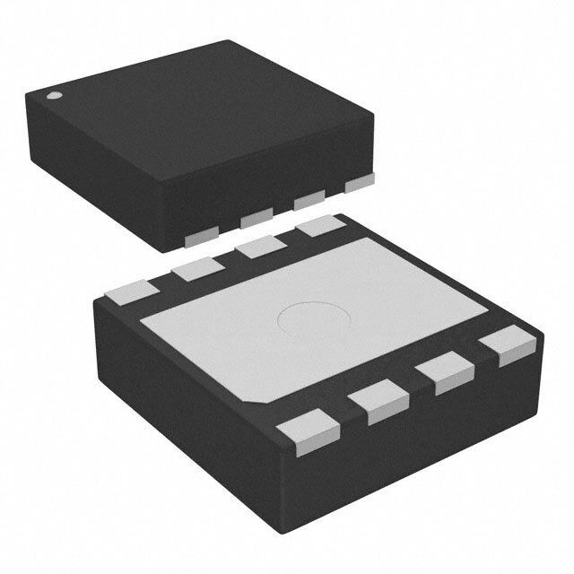
| 供应商器件封装 | 8-SON 裸露焊盘(3x3) |
| 其它名称 | 296-19860-1 |
| 制造商产品页 | http://www.ti.com/general/docs/suppproductinfo.tsp?distId=10&orderablePartNumber=ADS8325IDRBT |
| 包装 | 剪切带 (CT) |
| 安装类型 | 表面贴装 |
| 封装/外壳 | 8-VDFN 裸露焊盘 |
| 工作温度 | -40°C ~ 85°C |
| 数据接口 | SPI |
| 标准包装 | 1 |
| 特性 | - |
| 电压源 | 单电源 |
| 转换器数 | 1 |
| 输入数和类型 | 2 个单端,单极1 个差分,单极 |
| 配用 | /product-detail/zh/ADS8325EVM/296-18378-ND/809673 |
| 采样率(每秒) | 100k |


- 商务部:美国ITC正式对集成电路等产品启动337调查
- 曝三星4nm工艺存在良率问题 高通将骁龙8 Gen1或转产台积电
- 太阳诱电将投资9.5亿元在常州建新厂生产MLCC 预计2023年完工
- 英特尔发布欧洲新工厂建设计划 深化IDM 2.0 战略
- 台积电先进制程称霸业界 有大客户加持明年业绩稳了
- 达到5530亿美元!SIA预计今年全球半导体销售额将创下新高
- 英特尔拟将自动驾驶子公司Mobileye上市 估值或超500亿美元
- 三星加码芯片和SET,合并消费电子和移动部门,撤换高东真等 CEO
- 三星电子宣布重大人事变动 还合并消费电子和移动部门
- 海关总署:前11个月进口集成电路产品价值2.52万亿元 增长14.8%


PDF Datasheet 数据手册内容提取
(cid:2)(cid:17)(cid:14)(cid:14)(cid:20)(cid:2)(cid:14)(cid:13)(cid:18)(cid:12) (cid:4)(cid:14)(cid:13)(cid:8)(cid:17)(cid:7)(cid:16)(cid:15) ADS8325 (cid:10)(cid:14)(cid:13)(cid:11) (cid:5)(cid:9)(cid:19)(cid:6)(cid:15) (cid:3)(cid:12)(cid:15)(cid:16)(cid:14)(cid:17)(cid:11)(cid:9)(cid:12)(cid:16)(cid:15) ADS8325 ADS8325 SBAS226C–MARCH2002–REVISEDAUGUST2007 16-Bit, High-Speed, 2.7V to 5.5V microPower Sampling ANALOG-TO-DIGITAL CONVERTER FEATURES DESCRIPTION 1 • 16-BitsNoMissingCodes The ADS8325 is a 16-bit, sampling, Analog-to-Digital 23 • VeryLowNoise:3LSB (A/D) converter specified for a supply voltage range PP • ExcellentLinearity:±1.5LSBtyp from 2.7V to 5.5V. It requires very little power, even when operating at the full 100kHz data rate. At lower • microPower: data rates, the high speed of the device enables it to – 4.5mWat100kHz spend most of its time in the power-down mode. For example, the average power dissipation is less than – 1mWat10kHz 1mWata10kHzdatarate. • MSOP-8andSON-8Packages(SONPackage SizeSameas3x3QFN) The ADS8325 offers excellent linearity and very low noise and distortion. It also features a synchronous • 16-BitUpgradetothe12-BitADS7816and serial (SPI/SSI compatible) interface and a differential ADS7822 input. The reference voltage can be set to any level • Pin-CompatibleWiththeADS7816,ADS7822, withintherangeof2.5VtoV . DD ADS7826,ADS7827,ADS7829,andADS8320 Low power and small size make the ADS8325 ideal • Serial(SPI™/SSI)Interfaces for portable and battery-operated systems. It is also a perfect fit for remote data acquisition modules, APPLICATIONS simultaneous multichannel systems, and isolated • Battery-OperatedSystems data acquisition. The ADS8325 is available in • RemoteDataAcquisition MSOP-8 and SON-8 packages. The SON package sizeisthesameasa3x3QFNpackage. • IsolatedDataAcquisition • SimultaneousSampling,Multi-Channel Systems • IndustrialControls • Robotics • VibrationAnalysis SAR REF ADS8325 D OUT +IN CDAC Serial -IN Interface DCLOCK S/H Amp Comparator CS/SHDN 1 Pleasebeawarethatanimportantnoticeconcerningavailability,standardwarranty,anduseincriticalapplicationsof TexasInstrumentssemiconductorproductsanddisclaimerstheretoappearsattheendofthisdatasheet. SPIisatrademarkofMotorola,Inc. 2 Allothertrademarksarethepropertyoftheirrespectiveowners. 3 PRODUCTIONDATAinformationiscurrentasofpublicationdate. Copyright©2002–2007,TexasInstrumentsIncorporated Products conform to specifications per the terms of the Texas Instruments standard warranty. Production processing does not necessarilyincludetestingofallparameters.
ADS8325 www.ti.com SBAS226C–MARCH2002–REVISEDAUGUST2007 This integrated circuit can be damaged by ESD. Texas Instruments recommends that all integrated circuits be handled with appropriateprecautions.Failuretoobserveproperhandlingandinstallationprocedurescancausedamage. ESDdamagecanrangefromsubtleperformancedegradationtocompletedevicefailure.Precisionintegratedcircuitsmaybemore susceptibletodamagebecauseverysmallparametricchangescouldcausethedevicenottomeetitspublishedspecifications. PACKAGE/ORDERINGINFORMATION(1) MAXIMUM INTEGRAL NOMISSING SPECIFIED LINEARITY CODESERROR PACKAGE- PACKAGE TEMPERATURE PACKAGE ORDERING TRANSPORTMEDIA, PRODUCT ERROR(LSB) (LSB)(2) LEAD DESIGNATOR RANGE MARKING NUMBER QUANTITY ADS8325IDGKT TapeandReel,250 ADS8325I ±6 15 MSOP-8 DGK –40(cid:176)Cto+85(cid:176)C B25 ADS8325IDGKR TapeandReel,2500 ADS8325IBDGKT TapeandReel,250 ADS8325IB ±4 16 MSOP-8 DGK –40(cid:176)Cto+85(cid:176)C B25 ADS8325IBDGKR TapeandReel,2500 ADS8325IDRBT TapeandReel,250 ADS8325I ±6 15 SON-8 DRB –40(cid:176)Cto+85(cid:176)C B25 ADS8325IDRBR TapeandReel,2500 ADS8325IBDRBT TapeandReel,250 ADS8325IB ±4 16 SON-8 DRB –40(cid:176)Cto+85(cid:176)C B25 ADS8325IBDRBR TapeandReel,2500 (1) Forthemostcurrentspecificationsandpackageinformation,refertoourwebsiteatwww.ti.com. (2) NoMissingCodesErrorspecifiesa5Vpowersupplyandreferencevoltage. ABSOLUTE MAXIMUM RATINGS(1) Overoperatingfree-airtemperaturerange(unlessotherwisenoted) ADS8325 UNIT Supplyvoltage,DGNDtoV –0.3to6 V DD Analoginputvoltage(2) –0.3toV +0.3 V DD Referenceinputvoltage(2) –0.3toV +0.3 V DD Digitalinputvoltage(2) –0.3toV +0.3 V DD Inputcurrenttoanypinexceptsupply –20to20 mA Powerdissipation SeeDissipationRatingTable T Operatingvirtualjunctiontemperaturerange –40to+150 (cid:176) C J T Operatingfree-airtemperaturerange –40to+85 (cid:176) C A T Storagetemperaturerange –65to+150 (cid:176) C STG Leadtemperature1,6mm(1/16inch)fromcasefor10sec +260 (cid:176) C (1) Stressesbeyondthoselistedunderabsolutemaximumratingsmaycausepermanentdamagetothedevice.Thesearestressratings only,andfunctionaloperationofthedeviceattheseoranyotherconditionsbeyondthoseindicatedunderrecommendedoperating conditionsisnotimplied.Exposuretoabsolute-maximum-ratedconditionsofextendedperiodsmayaffectdevicereliability. (2) Allvoltagevaluesarewithrespecttogroundterminal. PACKAGE DISSIPATION RATINGS DERATINGFACTOR T ≤+25(cid:176) C T =+70(cid:176) C T =+85(cid:176) C A A A PACKAGE R R ABOVET =+25(cid:176) C POWERRATING POWERRATING POWERRATING θJC θJA A DGK 39.1(cid:176) C/W 206.3(cid:176) C/W 4.847mW/(cid:176) C 606mW 388mW 315mW DRB 5(cid:176) C/W 45.8(cid:176) C/W 3.7mW/C 370mW 204mW 148mW 2 SubmitDocumentationFeedback Copyright©2002–2007,TexasInstrumentsIncorporated ProductFolderLink(s):ADS8325
ADS8325 www.ti.com SBAS226C–MARCH2002–REVISEDAUGUST2007 EQUIVALENTINPUTCIRCUIT VDD 5R0OWN C(4SA0MpPFLE) VDD ShSuwt-iDtcohwn 20pF VDD ANALOG IN REF I/O 5kW GND GND GND Diode Turn-On Voltage: 0.35V Equivalent Reference Equivalent Digital Input/Output Circuit Equivalent Analog Input Circuit Input Circuit RECOMMENDED OPERATING CONDITIONS Overoperatingfree-airtemperaturerange(unlessotherwisenoted) MIN TYP MAX UNIT Low-voltagelevels 2.7 3.6 V Supplyvoltage,GNDtoV DD 5Vlogiclevels 4.5 5.0 5.5 V Referenceinputvoltage 2.5 V V DD –IN –0.3 0 0.5 V Analoginputvoltage +IN–(–IN) 0 V V REF T Operatingjunctiontemperaturerange –40 +125 (cid:176) C J ELECTRICAL CHARACTERISTICS: V = +5 V DD Overrecommendedoperatingfree-airtemperatureat–40(cid:176) Cto+85(cid:176) C,V =5V,–IN=GND,f =100kHz,andf = REF SAMPLE CLK 24· f ,unlessotherwisenoted. SAMPLE ADS8325I ADS8325IB PARAMETER TESTCONDITIONS MIN TYP MAX MIN TYP MAX UNIT ANALOGINPUT Full-scalerange FSR +IN–(–IN) 0 VREF 0 VREF V Operatingcommon-modesignal –0.3 0.5 –0.3 0.5 V Inputresistance –IN=GND 5 5 GΩ Inputcapacitance –IN=GND,duringsampling 45 45 pF Inputleakagecurrent –IN=GND ±50 ±50 nA Differentialinputcapacitance +INto–IN,duringsampling 20 20 pF Full-powerbandwidth FSBW FSsinewave,SINAD=–3dB 20 20 kHz DCACCURACY Resolution 16 16 Bits Nomissingcode NMC 15 16 Bits Integrallinearityerror INL ±3 ±6 ±1.5 ±4 LSB Offseterror VOS ±0.75 ±1.5 ±0.5 ±1 mV Offseterrordrift TCVOS ±0.2 ±0.2 ppm/(cid:176)C Gainerror GERR ±24 ±12 LSB Gainerrordrift TCGERR ±3 ±3 ppm/(cid:176)C Noise 20 20 μVRMS Power-supplyrejection 4.75V≤VDD≤5.25V 3 3 LSB SAMPLINGDYNAMICS Conversiontime tCONV 24kHz<fCLK≤2.4MHz 6.667 666.7 6.667 666.7 μs Acquisitiontime tAQ fCLK=2.4MHz 1.875 1.875 μs Throughputrate 100 100 kSPS Clockfrequency 0.024 2.4 0.024 2.4 MHz ACACCURACY Copyright©2002–2007,TexasInstrumentsIncorporated SubmitDocumentationFeedback 3 ProductFolderLink(s):ADS8325
ADS8325 www.ti.com SBAS226C–MARCH2002–REVISEDAUGUST2007 ELECTRICAL CHARACTERISTICS: V = +5 V (continued) DD Overrecommendedoperatingfree-airtemperatureat–40(cid:176) Cto+85(cid:176) C,V =5V,–IN=GND,f =100kHz,andf = REF SAMPLE CLK 24· f ,unlessotherwisenoted. SAMPLE ADS8325I ADS8325IB PARAMETER TESTCONDITIONS MIN TYP MAX MIN TYP MAX UNIT Totalharmonicdistortion THD 5VPPsinewave,at1kHz –100 –106 dB Spurious-freedynamic range SFDR 5VPPsinewave,at1kHz –100 –108 dB Signal-to-noiseratio SNR –90 –91 dB Signal-to-noise+distortion SINAD 5VPPsinewave,at1kHz –90 –91 dB Effectivenumberofbits ENOB 14.6 14.7 Bits VOLTAGEREFERENCEINPUT Referencevoltage 2.5 VDD+0.3 2.5 VDD+0.3 V CS=GND,fSAMPLE=0Hz 5 5 kΩ Referenceinputresistance CS=VDD 5 5 GΩ Referenceinput 20 20 pF capacitance 1 1.5 1 1.5 mA Referenceinputcurrent CS=VDD 0.1 0.1 μA DIGITALINPUTS(1) Logicfamily CMOS CMOS High-levelinputvoltage VIH 0.7· VDD VDD+0.3 0.7· VDD VDD+0.3 V Low-levelinputvoltage VIL –0.3 0.3· VDD –0.3 0.3· VDD V Inputcurrent IIN VI=VDDorGND ±50 ±50 nA Inputcapacitance CI 5 5 pF DIGITALOUTPUTS(1) Logicfamily CMOS CMOS High-leveloutputvoltage VOH VDD=4.5V,IOH=–100μA 4.44 4.44 V Low-leveloutputvoltage VOL VDD=4.5V,IOL=100μA 0.5 0.5 V High-impedance-state outputcurrent IOZ CS=VDD,VI=VDDorGND ±50 ±50 nA Outputcapacitance CO 5 5 pF Loadcapacitance CL 30 30 pF Dataformat StraightBinary StraightBinary (1) Appliesfor5.0Vnominalsupply:V (min)=4.5VandV (max)=5.5V. DD DD 4 SubmitDocumentationFeedback Copyright©2002–2007,TexasInstrumentsIncorporated ProductFolderLink(s):ADS8325
ADS8325 www.ti.com SBAS226C–MARCH2002–REVISEDAUGUST2007 ELECTRICAL CHARACTERISTICS: V = +2.7V DD Overrecommendedoperatingfree-airtemperatureat–40(cid:176) Cto+85(cid:176) C,V =+2.5V,–IN=GND,f =100kHz,andf REF SAMPLE CLK =24· f ,unlessotherwisenoted. SAMPLE ADS8325I ADS8325IB PARAMETER TESTCONDITIONS MIN TYP MAX MIN TYP MAX UNIT ANALOGINPUT Full-scalerange FSR +IN–(–IN) 0 VREF 0 VREF V Operatingcommon-modesignal –0.3 0.5 –0.3 0.5 V Inputresistance –IN=GND 5 5 GΩ Inputcapacitance –IN=GND,duringsampling 45 45 pF Inputleakagecurrent –IN=GND ±50 ±50 nA Differentialinputcapacitance +INto–IN,duringsampling 20 20 pF Full-powerbandwidth FSBW FSsinewave,SINAD=–3dB 4 4 kHz DCACCURACY Resolution 16 16 Bits Nomissingcode NMC 14 15 Bits Integrallinearityerror INL ±3 ±6 ±1.5 ±4 LSB Offseterror VOS ±0.75 ±1.5 ±0.5 ±1 mV Offseterrordrift TCVOS ±3 ±3 ppm/(cid:176)C Gainerror GERR ±33 ±16 LSB Gainerrordrift TCGERR ±0.3 ±0.3 ppm/(cid:176)C Noise 20 20 μVRMS Power-supplyrejection 2.7V≤VDD≤3.6V 7 7 LSB SAMPLINGDYNAMICS Conversiontime tCONV 24kHz<fCLK≤2.4MHz 6.667 666.7 6.667 666.7 μs Acquisitiontime tAQ fCLK=2.4MHz 1.875 1.875 μs Throughputrate 100 100 kSPS Clockfrequency 0.024 2.4 0.024 2.4 MHz ACACCURACY Totalharmonicdistortion THD 2.5VPPsinewave,at1kHz –94 –94 dB Spurious-freedynamicrange SFDR 2.5VPPsinewave,at1kHz –96 –96 dB Signal-to-noiseratio SNR –85 –86 dB Signal-to-noise+distortion SINAD 2.5VPPsinewave,at1kHz –85 –85.5 dB Effectivenumberofbits ENOB 13.8 13.9 Bits VOLTAGEREFERENCEINPUT Referencevoltage 2.5 VDD+0.3 2.5 VDD+0.3 V CS=GND,fSAMPLE=0Hz 5 5 kΩ Referenceinputresistance CS=VDD 5 5 GΩ Referenceinputcapacitance 20 20 pF 0.5 0.75 0.5 0.75 mA Referenceinputcurrent CS=VDD 0.1 0.1 μA DIGITALINPUTS(1) Logicfamily LVCMOS LVCMOS High-levelinputvoltage VIH VDD=3.6V 2 VDD+0.3 2 VDD+0.3 V Low-levelinputvoltage VIL VDD=2.7V –0.3 0.8 –0.3 0.8 V Inputcurrent IIN VI=VDDorGND ±50 ±50 nA Inputcapacitance CI 5 5 pF (1) Appliesfor3.0Vnominalsupply:V (min)=2.7VandV (max)=3.6V. DD DD Copyright©2002–2007,TexasInstrumentsIncorporated SubmitDocumentationFeedback 5 ProductFolderLink(s):ADS8325
ADS8325 www.ti.com SBAS226C–MARCH2002–REVISEDAUGUST2007 ELECTRICAL CHARACTERISTICS: V = +2.7V (continued) DD Overrecommendedoperatingfree-airtemperatureat–40(cid:176) Cto+85(cid:176) C,V =+2.5V,–IN=GND,f =100kHz,andf REF SAMPLE CLK =24· f ,unlessotherwisenoted. SAMPLE ADS8325I ADS8325IB PARAMETER TESTCONDITIONS MIN TYP MAX MIN TYP MAX UNIT DIGITALOUTPUTS(2) Logicfamily LVCMOS LVCMOS High-leveloutputvoltage VOH VDD=2.7V,IOH=–100μA VDD–0.2 VDD–0.2 V Low-leveloutputvoltage VOL VDD=2.7V,IOL=100μA 0.2 0.2 V High-impedance-stateoutput current IOZ CS=VDD,VI=VDDorGND ±50 ±50 ±50 nA Outputcapacitance CO 5 5 pF Loadcapacitance CL 30 30 pF Dataformat StraightBinary StraightBinary (2) Appliesfor3.0Vnominalsupply:V (min)=2.7VandV (max)=3.6V. DD DD ELECTRICAL CHARACTERISTICS Overrecommendedoperatingfree-airtemperatureat–40(cid:176) Cto+85(cid:176) C,V =V ,–IN=GND,f =100kHz,andf = REF DD SAMPLE CLK 24· f ,unlessotherwisenoted. SAMPLE ADS8325I ADS8325IB UNIT PARAMETER TESTCONDITIONS MIN TYP MAX MIN TYP MAX POWER-SUPPLYREQUIREMENTS Low-voltagelevels 2.7 3.6 2.7 3.6 V Powersupply VDD 5Vlogiclevels 4.5 5.5 4.5 5.5 V VDD=3V 0.75 1.5 0.75 1.5 mA Operatingsupplycurrent IDD VDD=5V 0.9 1.5 0.9 1.5 mA VDD=3V 0.1 0.1 μA Power-downsupplycurrent (IDD VDD=5V 0.2 0.2 μA VDD=3V 2.25 4.5 2.25 4.5 mW Powerdissipation VDD=5V 4.5 7.5 4.5 7.5 mW VDD=3V,CS=VDD 0.3 0.3 μW Powerdissipationinpower-down VDD=5V,CS=VDD 0.6 0.6 μW 6 SubmitDocumentationFeedback Copyright©2002–2007,TexasInstrumentsIncorporated ProductFolderLink(s):ADS8325
ADS8325 www.ti.com SBAS226C–MARCH2002–REVISEDAUGUST2007 PIN CONFIGURATIONS DGKPACKAGE MSOP (TOPVIEW) REF 1 8 +V DD +IN 2 7 DCLOCK ADS8325 -IN 3 6 D OUT GND 4 5 CS/SHDN DRBPACKAGE(1) SON (TOPVIEW) REF 1 8 +V DD +IN 2 7 DCLOCK ADS8325 -IN 3 6 D OUT GND 4 (Thermal Pad) 5 CS/SHDN (1) The thermal pad is internally connected to the substrate. This pad can be connected to the analog ground or left floating.Keepthethermalpadseparatefromthedigitalground,ifpossible. PINASSIGNMENTS PIN NAME NO. I/O(1) DESCRIPTION REF 1 AI ReferenceInput +IN 2 AI NoninvertingInput –IN 3 AI InvertingAnalogInput GND 4 P Ground CS/SHDN 5 DI Chipselectwhenlow;Shutdownmodewhenhigh. D 6 DO Theserialoutputdataword. OUT DCLOCK 7 DI Dataclocksynchronizestheserialdatatransferanddeterminesconversionspeed. +V 8 P Powersupply DD (1) AIisAnalogInput,DIisDigitalInput,DOisDigitalOutput,andPisPower-SupplyConnection. Copyright©2002–2007,TexasInstrumentsIncorporated SubmitDocumentationFeedback 7 ProductFolderLink(s):ADS8325
ADS8325 www.ti.com SBAS226C–MARCH2002–REVISEDAUGUST2007 TIMING INFORMATION t CYC CS/SHDN Power Down Sample Conversion t SUCS DCLOCK t CSD Use positive clock edge for data transfer DOUT Hi-Z 0 B15 B14 B13 B12 B11 B10 B9 B8 B7 B6 B5 B4 B3 B2 B1 B0(1) Hi-Z (MSB) (LSB) t t SMPL CONV NOTE: (1) A minimum of 22 clock cycles are required for 16-bit conversion; 24 clock cycles are shown. IfCSremains low at the end of conversion, a new data stream is shifted out with LSB-first data followed by zeroes indefinitely. t CYC CS/SHDN tSUCS Power Down DCLOCK t CSD DOUT Hi-Z 0 B15 B14 B6 B5 B4 B3 B2 B1 B0 B1 B2 B3 B4 B5 B0 B11B12 B13 B14 B1(52) Hi-Z (MSB) (LSB) (MSB) t t SMPL CONV NOTE: (2) After completing the data transfer, if further clocks are applied withCSlow, the A/D converter will output zeroes indefinitely. 1.4V 3kW 90% D OUT DOUT Test Point 10% t t 100pF r f C LOAD Voltage Waveforms for D Rise and Fall Times, t, t OUT r f Load Circuit for t , t, and t dDO r f Test Point DCLOCK V DD 3kW tdisWaveform 2, ten tdDO DOUT D 100pF tdisWaveform 1 OUT C LOAD t hDO Load Circuit for t and t dis en Voltage Waveforms for D Delay Times, t OUT dDO 90% CS/SHDN CS/SHDN DOUT 90% DCLOCK 1 4 5 Waveform 1(3) t dis DOUT 10% DOUT B15 Waveform 2(4) t en Voltage Waveforms for t dis Voltage Waveforms for t en NOTES:(3) Waveform 1 is for an output with internal conditions such that the output is high unless disabled by the output control. (4) Waveform 2 is for an output with internal conditions such that the output is low unless disabled by the output control. Figure1.TimingDiagramsandTestCircuitsfortheParamtersinTable1 8 SubmitDocumentationFeedback Copyright©2002–2007,TexasInstrumentsIncorporated ProductFolderLink(s):ADS8325
ADS8325 www.ti.com SBAS226C–MARCH2002–REVISEDAUGUST2007 TIMING INFORMATION (continued) Table1.TimingCharacteristics SYMBOL DESCRIPTION MIN TYP MAX UNIT t AnalogInputSampleTime 4.5 5.0 ClkCycles SMPL t ConversionTime 16 ClkCycles CONV t ThroughputRate 100 kHz CYC t CSFallingtoDCLOCKLOW 0 ns CSD t CSFallingtoDCLOCKRising 20 ns SUCS t DCLOCKFallingtoCurrentD NotValid 5 15 ns HDO OUT t CSRisingtoDOUT3-State 70 100 ns DIS t DCLOCKFallingtoD Enabled 20 50 ns EN OUT t D FallTime 5 25 ns F OUT t D RiseTime 7 25 ns R OUT Copyright©2002–2007,TexasInstrumentsIncorporated SubmitDocumentationFeedback 9 ProductFolderLink(s):ADS8325
ADS8325 www.ti.com SBAS226C–MARCH2002–REVISEDAUGUST2007 TYPICAL CHARACTERISTICS: V = +5V DD AtT =+25(cid:176) C,V =+5V,V =+5V,f =100kHz,f =24· f ,unlessotherwisenoted. A DD REF SAMPLE CLK SAMPLE INTEGRALLINEARITYERROR DIFFERENTIALLINEARITYERROR vsCODE vsCODE 3 3 2 2 1 1 S) S) B B E (LS 0 E (LS 0 IL -1 DL -1 -2 -2 -3 -3 0000 4000 8000 C000 FFFF 0000 4000 8000 C000 FFFF H H H H H H H H H H Output Code Output Code Figure2. Figure3. FREQUENCYSPECTRUM FREQUENCYSPECTRUM (8192PointFFT,f =1.0132kHz,–0.2dB) (8192PointFFT,f =10.0022kHz,–0.2dB) IN IN 0 0 -20 -20 -40 -40 dB) -60 dB) -60 e ( e ( ud -80 ud -80 mplit -100 mplit -100 A A -120 -120 -140 -140 -160 -160 0 10 20 30 40 50 0 10 20 30 40 50 Frequency (kHz) Frequency (kHz) Figure4. Figure5. SIGNAL-TO-NOISERATIOAND SPURIOUS-FREEDYNAMICRANGEAND SIGNAL-TO-NOISE+DISTORTION TOTALHARMONICDISTORTION vsINPUTFREQUENCY vsINPUTFREQUENCY 105 110 -110 SFDR 100 105 -105 SNR B) 95 100 -100 d SINAD ( 9805 R (dB) 9950 --9950 D (dB) and 80 SFD 85 -85 TH R N SINAD S 75 80 NOTE: (1) First nine -80 (1) harmonics of the THD 70 75 input frequency. -75 65 70 -70 1 10 100 245 1 10 100 245 Frequency (kHz) Frequency (kHz) Figure6. Figure7. 10 SubmitDocumentationFeedback Copyright©2002–2007,TexasInstrumentsIncorporated ProductFolderLink(s):ADS8325
ADS8325 www.ti.com SBAS226C–MARCH2002–REVISEDAUGUST2007 TYPICAL CHARACTERISTICS: V = +5V (continued) DD AtT =+25(cid:176) C,V =+5V,V =+5V,f =100kHz,f =24· f ,unlessotherwisenoted. A DD REF SAMPLE CLK SAMPLE SIGNAL-TO-NOISE+DISTORTION PEAK-TO-PEAKNOISEFORADCINPUT vsINPUTLEVEL vsREFERENCEVOLTAGE 100 200 f = 1.0132kHz IN B) 90 100 d n ( 80 B) o S storti 70 se (L oise + Di 6500 Peak Noi 10 gnal-to-N 4300 Peak-to- Si 20 10 1 -80 -70 -60 -50 -40 -30 -20 -10 0 0.1 1 5 Input Level (dB) Reference Voltage (V) Figure8. Figure9. EFFECTIVENUMBEROFBITS CHANGEINSIGNAL-TO-NOISE+DISTORTION vsINPUTFREQUENCY vsTEMPERATURE 15.0 0.4 f = 1.0132kHz,-0.2dB 14.5 IN 0.2 s Bit 14.0 B) ber of 13.5 5°C (d 0.0 Num 13.0 m +2 -0.2 Effective 1122..50 Delta fro -0.4 -0.6 11.5 11.0 -0.8 1 10 100 -50 -25 0 25 50 75 100 Frequency (kHz) Temperature (°C) Figure10. Figure11. CHANGEINGAIN CHANGEINUPO vsTEMPERATURE vsTEMPERATURE 2.0 3.0 1.5 2.5 SBS) 1.0 SBS) 2.0 C (L 0.5 C (L 1.5 25° 25° 1.0 m 0.0 m Delta fro -0.5 Delta fro 00..50 -1.0 -0.5 -1.5 -1.0 -50 -25 0 25 50 75 100 -50 -25 0 25 50 75 100 Temperature (°C) Temperature (°C) Figure12. Figure13. Copyright©2002–2007,TexasInstrumentsIncorporated SubmitDocumentationFeedback 11 ProductFolderLink(s):ADS8325
ADS8325 www.ti.com SBAS226C–MARCH2002–REVISEDAUGUST2007 TYPICAL CHARACTERISTICS: V = +5V (continued) DD AtT =+25(cid:176) C,V =+5V,V =+5V,f =100kHz,f =24· f ,unlessotherwisenoted. A DD REF SAMPLE CLK SAMPLE SUPPLYCURRENT vsTEMPERATURE 1.1 A) 1.0 m nt ( e urr 0.9 C y pl p u S 0.8 0.7 -50 -25 0 25 50 75 100 Temperature (°C) 12 SubmitDocumentationFeedback Copyright©2002–2007,TexasInstrumentsIncorporated ProductFolderLink(s):ADS8325
ADS8325 www.ti.com SBAS226C–MARCH2002–REVISEDAUGUST2007 TYPICAL CHARACTERISTICS: V = +2.7V DD AtT =+25(cid:176) C,V =2.7V,V =2.5V,f =100kHz,f =24· f ,unlessotherwisenoted. A DD REF SAMPLE CLK SAMPLE INTEGRALLINEARITYERROR DIFFERENTIALLINEARITYERROR vsCODE vsCODE 3 3 2 2 1 1 S) S) B B E (LS 0 E (LS 0 IL -1 DL -1 -2 -2 -3 -3 0000 4000 8000 C000 FFFF 0000 4000 8000 C000 FFFF H H H H H H H H H H Output Code Output Code Figure15. Figure16. FREQUENCYSPECTRUM FREQUENCYSPECTRUM (8192PointFFT,f =1.0132kHz,–0.2dB) (8192PointFFT,f =10.0022kHz,–0.2dB) IN IN 0 0 -20 -20 -40 -40 dB) -60 dB) -60 e ( e ( ud -80 ud -80 mplit -100 mplit -100 A A -120 -120 -140 -140 -160 -160 0 10 20 30 40 50 0 10 20 30 40 50 Frequency (kHz) Frequency (kHz) Figure17. Figure18. SIGNAL-TO-NOISERATIOAND SPURIOUS-FREEDYNAMICRANGEAND SIGNAL-TO-NOISE+DISTORTION TOTALHARMONICDISTORTION vsINPUTFREQUENCY vsINPUTFREQUENCY 95 100 -100 90 -90 85 SNR and SINAD (dB) 7655 SFDR (dB) 8700 SFDR --8700 THD (dB) R 60 -60 N S 55 SINAD 50 NhaOrmTEo:n (ic1s) Foifr stht enine THD(1) -50 input frequency. 45 40 -40 1 10 100 245 1 10 100 245 Frequency (kHz) Frequency (kHz) Figure19. Figure20. Copyright©2002–2007,TexasInstrumentsIncorporated SubmitDocumentationFeedback 13 ProductFolderLink(s):ADS8325
ADS8325 www.ti.com SBAS226C–MARCH2002–REVISEDAUGUST2007 TYPICAL CHARACTERISTICS: V = +2.7V (continued) DD AtT =+25(cid:176) C,V =2.7V,V =2.5V,f =100kHz,f =24· f ,unlessotherwisenoted. A DD REF SAMPLE CLK SAMPLE SIGNAL-TO-NOISE+DISTORTION EFFECTIVENUMBEROFBITS vsINPUTLEVEL vsINPUTFREQUENCY 100 14.5 fIN= 1.0132kHz 14.0 B) 90 13.5 on (d 80 Bits 1132..05 nal-to-Noise + Distorti 7654300000 Effective Number of 1111121100998........05050505 Sig 20 8.0 7.5 10 7.0 -80 -70 -60 -50 -40 -30 -20 -10 0 1 10 100 Input Level (dB) Frequency (kHz) Figure21. Figure22. CHANGEINSIGNAL-TO-NOISE+DISTORTION CHANGEINGAIN vsTEMPERATURE vsTEMPERATURE 0.4 2.0 f = 1.0132kHz,-0.2dB IN 1.5 0.2 5°C (dB) 0.0 C (LSBS) 10..05 m +2 -0.2 m 25° 0.0 Delta fro -0.4 Delta fro --01..50 -0.6 -1.5 -0.8 -2.0 -50 -25 0 25 50 75 100 -50 -25 0 25 50 75 100 Temperature (°C) Temperature (°C) Figure23. Figure24. CHANGEINUPO SUPPLYCURRENT vsTEMPERATURE vsTEMPERATURE 1.2 0.9 BS) 0.8 A) C (LS 0.4 nt (m 0.8 25° urre m C Delta fro-00..04 Supply 0.7 -0.8 0.6 -50 -25 0 25 50 75 100 -50 -25 0 25 50 75 100 Temperature (°C) Temperature (°C) 14 SubmitDocumentationFeedback Copyright©2002–2007,TexasInstrumentsIncorporated ProductFolderLink(s):ADS8325
ADS8325 www.ti.com SBAS226C–MARCH2002–REVISEDAUGUST2007 THEORY OF OPERATION ANALOG INPUT The ADS8325 is a classic Successive Approximation The analog input of ADS8325 is differential. The +IN Register (SAR) Analog-to-Digital (A/D) converter. The and –IN input pins allow for a differential input signal. architecture is based on capacitive redistribution that The amplitude of the input is the difference between inherently includes a sample-andhold function. The the +IN and –IN input, or (+IN) – (–IN). Unlike some converter is fabricated on a 0.6μ CMOS process. The converters of this type, the –IN input is not resampled architecture and process allow the ADS8325 to later in the conversion cycle. When the converter acquire and convert an analog signal at up to goes into the hold mode or conversion, the voltage 100,000 conversions per second while consuming difference between +IN and –IN is captured on the lessthan4.5mWfrom+V . internalcapacitorarray. DD The ADS8325 requires an external reference, an The range of the –IN input is limited to –0.3V to external clock, and a single power source (V ). The +0.5V.Duetothis,thedifferentialinput could be used DD external reference can be any voltage between 2.5V torejectsignalsthatarecommonto both inputs in the and 5.5V. The value of the reference voltage directly specified range. Thus, the –IN input is best used to sets the range of the analog input. The reference sense a remote signal ground that may move slightly input current depends on the conversion rate of the withrespecttothelocalgroundpotential. ADS8325. Thegeneralmethodfordrivingtheanaloginputof the The external clock can vary between 24kHz (1kHz ADS8325 is shown in Figure 26 and Figure 27. The throughput) and 2.4MHz (100kHz throughput). The –IN input is held at the common-mode voltage. The duty cycle of the clock is essentially unimportant as +IN input swings from –IN (or common-mode voltage) long as the minimum high and low times are at least to –IN + V (or commonmode voltage + V ), and REF REF 200ns (V = 4.75V or greater). The minimum clock the peak-to-peak amplitude is +V . The value of DD REF frequency is set by the leakage on the internal V determines the range over which the REF capacitorstotheADS8325. common-mode voltage may vary (see Figure 28). Figure 29 and Figure 30 illustrate the typical change The analog input is provided to two input pins: +IN in gain and offset as a function of the common-mode and –IN. When a conversion is initiated, the voltageappliedtothe–INpin. differential input on these pins is sampled on the internal capacitor array. While a conversion is in progress, both inputs are disconnected from any internalfunction. 0V to +VREF ADS8325 Peak-to-Peak The digital result of the conversion is clocked out by the DCLOCK input and is provided serially, most Common-Mode significant bit first, on the D pin. The digital data Voltage OUT that is provided on the D pin is for the conversion OUT currently in progress—there is no pipeline delay. It is Figure26.MethodsofDrivingtheADS8325 possible to continue to clock the ADS8325 after the conversion is complete and to obtain the serial data least significant bit first. See the Timing Information sectionformoreinformation. Common-Mode Voltage+ V +IN REF +V REF Common-ModeVoltage t -IN = Common-Mode Voltage NOTE:Themaximumdifferentialvoltagebetween+INand–INoftheADS8325isV .SeeFigure28forafurther REF explanationofthecommon-modevoltagerangefordifferentialinputs. Figure27.DifferentialInputModeoftheADS8325 Copyright©2002–2007,TexasInstrumentsIncorporated SubmitDocumentationFeedback 15 ProductFolderLink(s):ADS8325
ADS8325 www.ti.com SBAS226C–MARCH2002–REVISEDAUGUST2007 The input current required by the analog inputs nge (V) 1 VDD= 5V dvEoeslpstaeegnnetdi,aslslyoo,nutrhaceencuiummrrpebenedtraionnftcoefa,thcaetonArdsD:pSso8aw3me2pr5-ldecohrwaantreg,mesiondtpheue.t a e R 0.5 internal capacitor array during the sample period. g a After this capacitance has been fully charged, there is olt V 0 no further input current. The source of the analog e od -0.3 input voltage must be able to charge the input M n- capacitance (40pF) to a 16-bit settling level within 4.5 mo clock cycles (1.875μs). When the converter goes into m Co -1 the hold mode, or while it is in the power-down mode, theinputimpedanceisgreaterthan1GΩ. 2 2.5 3 4 4.8 5 6 VREF(V) Care must be taken regarding the absolute analog input voltage. To maintain the linearity of the Figure28.+INAnalogInput:Common-Mode converter,the–INinputshouldnotdropbelowGND – VoltageRangevsVREF 0.3V or exceed GND + 0.5V. The +IN input should always remain within the range of GND – 0.3V to V DD + 0.3V, or –IN to –IN + V , whichever limit is REF 60 reached first. Outside of these ranges, the converter's B) 50 VDD= 5V linearitymaynotmeetspecifications. S V = 4V V (L 40 REF To minimize noise, low bandwidth input signals with 0 lowpass filters should be used. In each case, care = CM 30 should be taken to ensure that the output impedance o V of the sources driving the +IN and –IN inputs are e t 20 matched.Often,asmallcapacitor(20pF)betweenthe v ati positive and negative inputs helps to match their el 10 R impedance. To obtain maximum performance from a elt 0 the ADS8325, the input circuit from Figure 31 is D recommended. -10 -0.4 -0.3 -0.2 -0.1 0.0 0.1 0.2 0.3 0.4 0.5 0.6 0.7 V (V) CM Figure29.ChangeinGainvsCommon-Mode Voltage CHANGE IN UPO vs COMMON-MODE VOLTAGE 30 V = 5V S) VDD = 4V B REF S 20 L V ( 0 = 10 M C V o e t 0 v ati el R a -10 elt D -20 -0.4 -0.3 -0.2 -0.1 0.0 0.1 0.2 0.3 0.4 0.5 0.6 0.7 V (V) CM Figure30.ChangeinUnipolarOffsetvs Common-ModeVoltage 16 SubmitDocumentationFeedback Copyright©2002–2007,TexasInstrumentsIncorporated ProductFolderLink(s):ADS8325
ADS8325 www.ti.com SBAS226C–MARCH2002–REVISEDAUGUST2007 50W +IN 50W 40pF 50W +IN 50W 40pF OPA365 OPA365 100pF 100pF ADS8325 1nF ADS8325 -IN 50W 40pF 50W -IN 50W 40pF OPA365 100pF Single-Ended Differential Figure31.Single-EndedandDifferentialMethodsofInterfacingtheADS8325 As the difference between the power-supply voltage REFERENCE INPUT and reference voltage increases, the gain and offset The external reference sets the analog input range. performance of the converter will decrease. Figure 32 The ADS8325 will operate with a reference in the shows the typical change in gain and offset as a range of 2.5V to V . There are several important function of the difference between the power-supply DD implicationstothis. voltage and reference voltage. For the combination of V = 2.7V and V = 2.5V, or V = 5V and V = As the reference voltage is reduced, the analog DD REF DD REF 5V, offset and gain error will be minimal. The most voltage weight of each digital output code is reduced. dramatic difference in offset can be seen when V = This is often referred to as the Least Significant Bit DD 5VandV =2.5V. (LSB) size and is equal to the reference voltage REF divided by 65,536. This means that any offset or gain CHANGE IN OFFSET AND GAIN vs error inherent in the A/D converter will appear to SUPPLY/REFERENCE DIFFERENTIAL increase, in terms of LSB size, as the reference 3.0 voltage is reduced. For a reference voltage of 2.5V, the value of LSB is 38.15μV, and for reference 2.5 voltageof5V,theLSBis76.3μV. 2.0 TinhcerenaosiesewinithhelroewnetrinLtSheBcsoiznev.erWteirthwiall a5lVsoraepfepreeanrcteo, mV) 1.5 Offset a ( theinternalnoiseoftheconvertertypicallycontributes elt 1.0 only 1.5LSBs peak-to-peak of potential error to the D Gain output code. When the external reference is 2.5V, the 0.5 potential error contribution from the internal noise will 0 be 2 times larger (3LSBs). The errors due to the internal noise are Gaussian in nature and can be -0.5 reducedbyaveragingconsecutiveconversionresults. 0 0.25 0.50 0.75 1.001.25 1.50 1.75 2.00 2.25 2.50 2.75 V to V (V) For more information regarding noise, consult DD REF Figure 9, Peak-to-Peak Noise vs Reference Voltage. Figure32.ChangeinOffsetandGainvsthe Note that Figure 10, Effective Number Of Bits vs DifferenceBetweenPower-SupplyandReference Input Frequency, is calculated based on the Voltage converter’s signal-to-(noise + distortion) ratio with a 1kHz, 0dB input signal. SINAD is related to ENOB as follows: SINAD=6.02· ENOB+1.76 Copyright©2002–2007,TexasInstrumentsIncorporated SubmitDocumentationFeedback 17 ProductFolderLink(s):ADS8325
ADS8325 www.ti.com SBAS226C–MARCH2002–REVISEDAUGUST2007 With lower reference voltages, extra care should be dividing the number of codes measured by 6 and this taken to provide a clean layout including adequate will yield the ±3σ distribution, or 99.7%, of all codes. bypassing, a clean power supply, a low-noise Statistically, up to three codes could fall outside the reference, and a low-noise input signal. Due to the distribution when executing 1000 conversions. The lower LSB size, the converter will also be more ADS8325, with < 3 output codes for the ±3σ sensitive to external sources of error, such as nearby distribution,willyielda<±0.5LSBsoftransition noise. digitalsignalsandelectromagneticinterference. Remember, to achieve this low-noise performance, the peak-to-peak noise of the input signal and The equivalent input circuit for the reference voltage referencemustbe<50μV. is presented in Figure 33. The 5kΩ resistor presents a constant load during the conversion process. At the 4005 same time, an equivalent capacitor of 20pF is switched. To obtain optimum performance from the V = 5.0V DD ADS8325, special care must be taken in designing V = 5.0V REF the interface circuit to the reference input pin. To ensure a stable reference voltage, a 47μF tantalum capacitor with low ESR should be connected as close as possible to the input pin. If a high output impedance reference source is used, an additional operational amplifier with a current limiting resistor mustbeplacedinfrontofthecapacitors. 519 476 ADS8325 0 0 7FFD 7FFE 7FFF 8000 8001 20pF 100W VREF Code OPA340 47mF 5kW Figure34.5000ConversionHistogramofaDC Input VDD= 2.7V 3499 V = 2.5V Figure33.InputReferenceCircuitandits REF Interface WhentheADS8325isinpower-down mode, the input resistance of the reference pin will have a value of 5GΩ. Since the input capacitors must be recharged before the next conversion starts, an operational amplifier with good dynamic characteristics must be usedtobufferthereferenceinput. 683 NOISE 649 The transition noise of the ADS8325 itself is 90 79 extremely low (see Figure 34 and Figure 35); it is 7FFD 7FFE 7FFF 8000 8001 much lower than competing A/D converters. These Code histograms were generated by applying a low-noise DC input and initiating 5000 conversions. The digital Figure35.5000ConversionHistogramofaDC output of the A/D converter will vary in output code Input due to the internal noise of the ADS8325. This is true for all 16-bit, SAR-type A/D converters. Using a histogram to plot the output codes, the distribution should appear bell-shaped with the peak of the bell curve representing the nominal code for the input value. The ±1σ, ±2σ, and ±3σ distributions will representthe68.3%,95.5%,and 99.7%, respectively, ofallcodes.The transition noise can be calculated by 18 SubmitDocumentationFeedback Copyright©2002–2007,TexasInstrumentsIncorporated ProductFolderLink(s):ADS8325
ADS8325 www.ti.com SBAS226C–MARCH2002–REVISEDAUGUST2007 AVERAGING SERIALINTERFACE The noise of the A/D converter can be compensated The ADS8325 communicates with microprocessors by averaging the digital codes. By averaging and other digital systems via a synchronous 3-wire conversion results, transition noise will be reduced by serial interface, as illustrated in the Timing a factor of 1/√n, where n is the number of averages. Information section. The DCLOCK signal For example, averaging four conversion results will synchronizes the data transfer with each bit being reduce the transition noise from ±0.5LSB to transmitted on the falling edge of DCLOCK. Most ±0.25LSB. Averaging should only be used for input receiving systems will capture the bitstream on the signalswithfrequenciesnearDC. rising edge of DCLOCK. However, if the minimum hold time for D is acceptable, the system can use For AC signals, a digital filter can be used to OUT thefallingedgeofDCLOCKtocaptureeachbit. low-pass filter and decimate the output codes. This works in a similar manner to averaging; for every A falling CS signal initiates the conversion and data decimation by 2, the signal-to-noise ratio will improve transfer. The first 4.5 to 5.0 clock periods of the 3dB. conversion cycle are used to sample the input signal. After the fifth falling DCLOCK edge, D is enabled OUT DIGITAL INTERFACE and will output a LOW value for one clock period. For the next 16 DCLOCK periods, D will output the OUT SIGNALLEVELS conversion result, most significant bit first. After the least significant bit (B0) has been output, subsequent The ADS8325 has a wide range of power-supply clocks will repeat the output data, but in a least voltage. The A/D converter, as well as the digital significantbitfirstformat. interface circuit, is designed to accept and operate from 2.7V up to 5.5V. This voltage range will After the most significant bit (B15) has been accommodatedifferentlogiclevels. repeated, D will tri-state. Subsequent clocks will OUT have no effect on the converter. A new conversion is When the ADS8325's power-supply voltage is in the initiated only when CS has been taken HIGH and range of 4.5V to 5.5V (5V logic level), the ADS8325 returnedLOW. can be connected directly to another 5V CMOS integratedcircuit. DATAFORMAT Another possibility is that the ADS8325's The output data from the ADS8325 is in Straight power-supply voltage is in the range of 2.7V to 3.6V. Binary format (see Figure 36. This figure represents The ADS8325 can be connected directly to another the ideal output code for a given input voltage and 3.3VLVCMOSintegratedcircuit. does not include the effects of offset, gain error, or noise. Copyright©2002–2007,TexasInstrumentsIncorporated SubmitDocumentationFeedback 19 ProductFolderLink(s):ADS8325
ADS8325 www.ti.com SBAS226C–MARCH2002–REVISEDAUGUST2007 Straight Binary 1111 1111 1111 1111 65535 1111 1111 1111 1111 65534 1111 1111 1111 1111 65533 e d o ut C 1000 0000 0000 0001 32769 al Outp 1000 0000 0000 0000 32768 Step git Di 0111 1111 1111 1111 32767 0000 0000 0000 0010 2 0000 0000 0000 0001 1 0000 0000 0000 0000 0 V = V = 0V 2.499962V 2.500038V V = V + V = 5V Z CM FS CM REF 38.15mV V -1LSB = 4.999924V FS V = V + V /2 = 2.5V MS CM REF 76.29mV 4.999847V Unipolar Analog Input Voltage 152.58mV 1LSB = 76.29mV V = 0V CM 16-BIT V = 5V REF Straight Binary Output Unipolar Analog Input Zero Code V = 0000H V = V Z CODE CM Midscale Code V = 8000H V = V + V /2 MS CODE CM REF Full-Scale Code V = FFFFH V = (V + V )-1LSB FS CODE CM REF Figure36.IdealConversionCharacteristics(Condition:V =0V,V =5V) CM REF 20 SubmitDocumentationFeedback Copyright©2002–2007,TexasInstrumentsIncorporated ProductFolderLink(s):ADS8325
ADS8325 www.ti.com SBAS226C–MARCH2002–REVISEDAUGUST2007 POWER DISSIPATION POWER SUPPLY AND REFERENCE CURRENT vs SAMPLE RATE The architecture of the converter, the semiconductor 1000 fabrication process, and a careful design, allow the T = 25°C A I ADS8325 to convert at up to a 100kHz rate while VDD= 5.0V DD requiring very little power. However, for the absolute VREF= 5.0V F = 2.4MHz lowest power dissipation, there are several things to CLK 100 keepinmind. A) m The power dissipation of the ADS8325 scales directly ent ( with conversion rate. Therefore, the first step to Curr IREF 10 achieving the lowest power dissipation is to find the lowest conversion rate that will satisfy the requirementsofthesystem. In addition, the ADS8325 is in power-down mode 1 under two conditions: when the conversion is 10 100 complete and whenever CS is HIGH (see the Timing Sample Rate (kHz) Information section). Ideally, each conversion should occur as quickly as possible, preferably at a 2.4MHz Figure37.Power-SupplyandReferenceCurrent clock rate. This way, the converter spends the vsSampleRateatVDD=5V longest possible time in the power-down mode. This is very important as the converter not only uses power on each DCLOCK transition (as is typical for POWER SUPPLY AND REFERENCE CURRENT vs SAMPLE RATE digital CMOS components), but also uses some 1000 current for the analog circuitry, such as the T = 25°C A I comparator. The analog section dissipates power VDD= 2.7V DD V = 2.5V continuouslyuntilthepower-downmodeisentered. REF F = 2.4MHz CLK 100 See Figure 37 and Figure 38 for the current A) cthoensseumgpratipohnso,ftthhee AcDonSv8e3r2te5rviesrsculoscskaemdplaetra2t.e4.MFHozr ent (m regardless of the sample rate. CS is held HIGH Curr IREF 10 duringtheremainingsampleperiod. There is an important distinction between the power-down mode that is entered after a conversion is complete and the full power-down mode that is 1 10 100 enabled when CS is HIGH. CS LOW will shut down Sample Rate (kHz) only the analog section. The digital section is completely shut down only when CS is HIGH. Thus, if CS is left LOW at the end of a conversion, and the Figure38.Power-SupplyandReferenceCurrent vsSampleRateatV =2.7V converter is continually clocked, the power DD consumptionwillnotbeaslowaswhenCSisHIGH. This technique can be used to lower the power SHORTCYCLING dissipation (or to increase the conversion rate) in Another way to save power is to utilize the CS signal those applications where an analog signal is being to short cycle the conversion. Due to the ADS8325 monitored until some condition becomes true. For placing the latest data bit on the D line as it is example, if the signal is outside a predetermined OUT generated, the converter can easily be short cycled. range, the full 16-bit conversion result may not be This term means that the conversion can be needed. If so, the conversion can be terminated after terminated at any time. For example, if only 14 bits of the first n bits, where n might be as low as 3 or 4. theconversionresultareneeded,thentheconversion This results in lower power dissipation in both the can be terminated (by pulling CS HIGH ) after the converter and the rest of the system as they spend 14thbithasbeenclockedout. moretimeinpower-downmode. Copyright©2002–2007,TexasInstrumentsIncorporated SubmitDocumentationFeedback 21 ProductFolderLink(s):ADS8325
ADS8325 www.ti.com SBAS226C–MARCH2002–REVISEDAUGUST2007 LAYOUT resistor can help in this case). Keep in mind that while the ADS8325 draws very little current from the For optimum performance, care should be taken with reference on average, there are still instantaneous the physical layout of the ADS8325 circuitry. This will current demands placed on the external input and be particularly true if the reference voltage is low referencecircuitry. and/or the conversion rate is high. At a 100kHz conversion rate, the ADS8325 makes a bit decision Texas Instruments' OPA627 op amp provides every 416ns. That is, for each subsequent bit optimum performance for buffering both the signal decision, the digital output must be updated with the and reference inputs. For low-cost, low-voltage, results of the last bit decision, the capacitor array single-supply applications, the OPA2350 or OPA2340 appropriately switched and charged, and the input to dualopampsarerecommended. the comparator settled to a 16-bit level all within one Also, keep in mind that the ADS8325 offers no clockcycle.6 inherent rejection of noise or voltage variation in The basic SAR architecture is sensitive to spikes on regards to the reference input. This is of particular the power supply, reference, and ground connections concern when the reference input is tied to the power that occur just prior to latching the comparator output. supply. Any noise and ripple from the supply will Thus, during any single conversion for an n-bit SAR appear directly in the digital results. While converter, there are n windows in which large high-frequency noise can be filtered out as described external transient voltages can easily affect the in the previous paragraph, voltage variation due to conversion result. Such spikes might originate from the line frequency (50Hz or 60Hz) can be difficult to switching power supplies, digital logic, and remove. high-power devices, to name a few. This particular The GND pin on the ADS8325 should be placed on a source of error can be very difficult to track down if clean ground point. In many cases, this will be the the glitch is almost synchronous to the converter's analog ground. Avoid connecting the GND pin too DCLOCK signal as the phase difference between the close to the grounding point for a microprocessor, two changes with time and temperature, causing microcontroller, or digital signal processor. If needed, sporadicmisoperation. run a ground trace directly from the converter to the With this in mind, power to the ADS8325 should be power-supply connection point. The ideal layout will clean and well-bypassed. A 0.1μF ceramic bypass include an analog ground plane for the converter and capacitor should be placed as close as possible to associatedanalogcircuitry. the ADS8325 package. In addition, a 1μF to 10μF capacitor and a 5Ω or 10Ω series resistor may be usedtolow-passfilteranoisysupply. The reference should be similarly bypassed with a 47μF capacitor. Again, a series resistor and large capacitor can be used to low-pass filter the reference voltage. If the reference voltage originates from an op amp, make sure that the op amp can drive the bypass capacitor without oscillation (the series 22 SubmitDocumentationFeedback Copyright©2002–2007,TexasInstrumentsIncorporated ProductFolderLink(s):ADS8325
ADS8325 www.ti.com SBAS226C–MARCH2002–REVISEDAUGUST2007 APPLICATION CIRCUITS high-frequency noise from the supply itself. The exact values should be picked such that the filter provides Figure 39 shows a basic data acquisition system. The adequate rejection of noise. Operational amplifiers ADS8325inputrangeisconnectedto 2.5V or 4.096V. and voltage reference are connected to analog power The 5Ω resistor and 1μF to 10μF capacitor filters the supply,AV . microcontroller noise on the supply, as well as any DD DV DD 2.7V to 3.6V + 0.1mF 10mF AV DD 2.7V to 5V 5W REF5025 IN OUT REF V DD + 0.47mF GND 4.7mF 0.1mF 10mF ADS8325 DSP 50W TMS320C6xx OPA365 +IN or V + (0V to 2.5V) TMS320C5xx CM 100pF CS or TMS320C2xx 1nF D OUT DCLOCK 50W OPA365 -IN GND GND V CM 100pF DV DD 4.5V to 5.5V + 0.1mF 10mF AV DD 4.3V to 5.5V 5W REF5040 IN OUT REF V DD + 0.47mF GND 4.7mF 0.1mF 10mF ADS8325 50W Microcontroller OPA365 +IN or 0V to 4.096V DSP 100pF CS D OUT DCLOCK -IN GND GND Figure39.TwoExamplesofaBasicDataAcquisitionSystem Copyright©2002–2007,TexasInstrumentsIncorporated SubmitDocumentationFeedback 23 ProductFolderLink(s):ADS8325
ADS8325 www.ti.com SBAS226C–MARCH2002–REVISEDAUGUST2007 Revision History ChangesfromRevisionB(June2007)toRevisionC .................................................................................................... Page • ChangednoteforDRBpackage............................................................................................................................................ 7 • Changedsecondtimingdiagramfromthetop;movedHi-Ztospantheentirerangeoft ............................................. 8 SMPL ChangesfromRevisionA(June2003)toRevisionB .................................................................................................... Page • Changedformatofdocumenttocurrentstandardlook......................................................................................................... 1 • ChangedR andC valuesinEquivalentInputCircuit.............................................................................................. 3 ON (SAMPLE) • AddedmissingvaluefromDigitalInputs,InputCurrent,BGrade(typo)............................................................................... 3 • AddedmissingvaluesfromSamplingDynamics,BGrade(typo)......................................................................................... 5 • ChangedDRBpackagepinoutdrawingtoincludethermalpadoutline(nottoscale).......................................................... 7 • Changedtimingdiagram(addednewdiagramtoexistingfigures)....................................................................................... 8 • AddedPeak-to-PeakNoiseForaDCInputvsReferenceVoltageplot ............................................................................. 11 • Changedinputcapcitancefrom20pFto40pF(regardingthesourceoftheanaloginputvoltage).................................... 16 • ChangedFigure31 ............................................................................................................................................................. 17 • ChangedFigure33capacitorfrom47Fto47μF(typo)....................................................................................................... 18 • ChangedV from7FFFHtoFFFFHinFigure36............................................................................................................... 20 FS • ChangedFigure39 ............................................................................................................................................................. 23 24 SubmitDocumentationFeedback Copyright©2002–2007,TexasInstrumentsIncorporated ProductFolderLink(s):ADS8325
PACKAGE OPTION ADDENDUM www.ti.com 6-Aug-2007 PACKAGING INFORMATION OrderableDevice Status(1) Package Package Pins Package EcoPlan(2) Lead/BallFinish MSLPeakTemp(3) Type Drawing Qty ADS8325IBDGKR ACTIVE MSOP DGK 8 2500 Green(RoHS& CUNIPDAU Level-2-260C-1YEAR noSb/Br) ADS8325IBDGKRG4 ACTIVE MSOP DGK 8 2500 Green(RoHS& CUNIPDAU Level-2-260C-1YEAR noSb/Br) ADS8325IBDGKT ACTIVE MSOP DGK 8 250 Green(RoHS& CUNIPDAU Level-2-260C-1YEAR noSb/Br) ADS8325IBDGKTG4 ACTIVE MSOP DGK 8 250 Green(RoHS& CUNIPDAU Level-2-260C-1YEAR noSb/Br) ADS8325IBDRBR ACTIVE SON DRB 8 2500 Green(RoHS& CUNIPDAU Level-2-260C-1YEAR noSb/Br) ADS8325IBDRBRG4 ACTIVE SON DRB 8 2500 Green(RoHS& CUNIPDAU Level-2-260C-1YEAR noSb/Br) ADS8325IBDRBT ACTIVE SON DRB 8 250 Green(RoHS& CUNIPDAU Level-2-260C-1YEAR noSb/Br) ADS8325IBDRBTG4 ACTIVE SON DRB 8 250 Green(RoHS& CUNIPDAU Level-2-260C-1YEAR noSb/Br) ADS8325IDGKR ACTIVE MSOP DGK 8 2500 Green(RoHS& CUNIPDAU Level-2-260C-1YEAR noSb/Br) ADS8325IDGKT ACTIVE MSOP DGK 8 250 Green(RoHS& CUNIPDAU Level-2-260C-1YEAR noSb/Br) ADS8325IDGKTG4 ACTIVE MSOP DGK 8 250 Green(RoHS& CUNIPDAU Level-2-260C-1YEAR noSb/Br) ADS8325IDRBR ACTIVE SON DRB 8 2500 Green(RoHS& CUNIPDAU Level-2-260C-1YEAR noSb/Br) ADS8325IDRBRG4 ACTIVE SON DRB 8 2500 Green(RoHS& CUNIPDAU Level-2-260C-1YEAR noSb/Br) ADS8325IDRBT ACTIVE SON DRB 8 250 Green(RoHS& CUNIPDAU Level-2-260C-1YEAR noSb/Br) ADS8325IDRBTG4 ACTIVE SON DRB 8 250 Green(RoHS& CUNIPDAU Level-2-260C-1YEAR noSb/Br) (1)Themarketingstatusvaluesaredefinedasfollows: ACTIVE:Productdevicerecommendedfornewdesigns. LIFEBUY:TIhasannouncedthatthedevicewillbediscontinued,andalifetime-buyperiodisineffect. NRND:Notrecommendedfornewdesigns.Deviceisinproductiontosupportexistingcustomers,butTIdoesnotrecommendusingthispartin anewdesign. PREVIEW:Devicehasbeenannouncedbutisnotinproduction.Samplesmayormaynotbeavailable. OBSOLETE:TIhasdiscontinuedtheproductionofthedevice. (2)EcoPlan-Theplannedeco-friendlyclassification:Pb-Free(RoHS),Pb-Free(RoHSExempt),orGreen(RoHS&noSb/Br)-pleasecheck http://www.ti.com/productcontentforthelatestavailabilityinformationandadditionalproductcontentdetails. TBD:ThePb-Free/Greenconversionplanhasnotbeendefined. Pb-Free(RoHS):TI'sterms"Lead-Free"or"Pb-Free"meansemiconductorproductsthatarecompatiblewiththecurrentRoHSrequirements forall6substances,includingtherequirementthatleadnotexceed0.1%byweightinhomogeneousmaterials.Wheredesignedtobesoldered athightemperatures,TIPb-Freeproductsaresuitableforuseinspecifiedlead-freeprocesses. Pb-Free(RoHSExempt):ThiscomponenthasaRoHSexemptionforeither1)lead-basedflip-chipsolderbumpsusedbetweenthedieand package, or 2) lead-based die adhesive used between the die and leadframe. The component is otherwise considered Pb-Free (RoHS compatible)asdefinedabove. Green(RoHS&noSb/Br):TIdefines"Green"tomeanPb-Free(RoHScompatible),andfreeofBromine(Br)andAntimony(Sb)basedflame retardants(BrorSbdonotexceed0.1%byweightinhomogeneousmaterial) (3) MSL, Peak Temp. -- The Moisture Sensitivity Level rating according to the JEDEC industry standard classifications, and peak solder temperature. Addendum-Page1
PACKAGE OPTION ADDENDUM www.ti.com 6-Aug-2007 Important Information and Disclaimer:The information provided on this page represents TI's knowledge and belief as of the date that it is provided. TI bases its knowledge and belief on information provided by third parties, and makes no representation or warranty as to the accuracy of such information. Efforts are underway to better integrate information from third parties. TI has taken and continues to take reasonable steps to provide representative and accurate information but may not have conducted destructive testing or chemical analysis on incomingmaterialsandchemicals.TIandTIsuppliersconsidercertaininformationtobeproprietary,andthusCASnumbersandotherlimited informationmaynotbeavailableforrelease. InnoeventshallTI'sliabilityarisingoutofsuchinformationexceedthetotalpurchasepriceoftheTIpart(s)atissueinthisdocumentsoldbyTI toCustomeronanannualbasis. Addendum-Page2
PACKAGE MATERIALS INFORMATION www.ti.com 6-Aug-2007 TAPE AND REEL INFORMATION PackMaterials-Page1
PACKAGE MATERIALS INFORMATION www.ti.com 6-Aug-2007 Device Package Pins Site Reel Reel A0(mm) B0(mm) K0(mm) P1 W Pin1 Diameter Width (mm) (mm) Quadrant (mm) (mm) ADS8325IBDGKR DGK 8 MLA 330 12 5.2 3.3 1.6 12 12 NONE ADS8325IBDGKT DGK 8 MLA 330 12 5.2 3.3 1.6 12 12 NONE ADS8325IBDRBR DRB 8 TUA 330 12 3.3 3.3 1.1 8 12 Q2 ADS8325IBDRBT DRB 8 TUA 330 12 3.3 3.3 1.1 8 12 Q2 ADS8325IDGKR DGK 8 MLA 330 12 5.2 3.3 1.6 12 12 NONE ADS8325IDGKT DGK 8 MLA 330 12 5.2 3.3 1.6 12 12 NONE ADS8325IDRBR DRB 8 TUA 330 12 3.3 3.3 1.1 8 12 Q2 ADS8325IDRBT DRB 8 TUA 330 12 3.3 3.3 1.1 8 12 Q2 TAPE AND REEL BOX INFORMATION Device Package Pins Site Length(mm) Width(mm) Height(mm) ADS8325IBDGKR DGK 8 MLA 390.0 348.0 63.0 ADS8325IBDGKT DGK 8 MLA 390.0 348.0 63.0 ADS8325IBDRBR DRB 8 TUA 0.0 0.0 0.0 ADS8325IBDRBT DRB 8 TUA 0.0 0.0 0.0 ADS8325IDGKR DGK 8 MLA 390.0 348.0 63.0 ADS8325IDGKT DGK 8 MLA 390.0 348.0 63.0 ADS8325IDRBR DRB 8 TUA 0.0 0.0 0.0 ADS8325IDRBT DRB 8 TUA 0.0 0.0 0.0 PackMaterials-Page2
PACKAGE MATERIALS INFORMATION www.ti.com 6-Aug-2007 PackMaterials-Page3
None
None
None
None
PACKAGE MATERIALS INFORMATION www.ti.com 9-Jul-2017 TAPE AND REEL INFORMATION *Alldimensionsarenominal Device Package Package Pins SPQ Reel Reel A0 B0 K0 P1 W Pin1 Type Drawing Diameter Width (mm) (mm) (mm) (mm) (mm) Quadrant (mm) W1(mm) ADS8325IBDGKR VSSOP DGK 8 2500 330.0 12.4 5.3 3.4 1.4 8.0 12.0 Q1 ADS8325IBDGKT VSSOP DGK 8 250 180.0 12.4 5.3 3.4 1.4 8.0 12.0 Q1 ADS8325IBDRBT SON DRB 8 250 180.0 12.4 3.3 3.3 1.1 8.0 12.0 Q2 ADS8325IDGKR VSSOP DGK 8 2500 330.0 12.4 5.3 3.4 1.4 8.0 12.0 Q1 ADS8325IDGKT VSSOP DGK 8 250 180.0 12.4 5.3 3.4 1.4 8.0 12.0 Q1 ADS8325IDRBR SON DRB 8 2500 330.0 12.4 3.3 3.3 1.1 8.0 12.0 Q2 ADS8325IDRBT SON DRB 8 250 180.0 12.4 3.3 3.3 1.1 8.0 12.0 Q2 PackMaterials-Page1
PACKAGE MATERIALS INFORMATION www.ti.com 9-Jul-2017 *Alldimensionsarenominal Device PackageType PackageDrawing Pins SPQ Length(mm) Width(mm) Height(mm) ADS8325IBDGKR VSSOP DGK 8 2500 367.0 367.0 35.0 ADS8325IBDGKT VSSOP DGK 8 250 210.0 185.0 35.0 ADS8325IBDRBT SON DRB 8 250 210.0 185.0 35.0 ADS8325IDGKR VSSOP DGK 8 2500 367.0 367.0 35.0 ADS8325IDGKT VSSOP DGK 8 250 210.0 185.0 35.0 ADS8325IDRBR SON DRB 8 2500 367.0 367.0 35.0 ADS8325IDRBT SON DRB 8 250 210.0 185.0 35.0 PackMaterials-Page2
IMPORTANTNOTICE TexasInstrumentsIncorporated(TI)reservestherighttomakecorrections,enhancements,improvementsandotherchangestoits semiconductorproductsandservicesperJESD46,latestissue,andtodiscontinueanyproductorserviceperJESD48,latestissue.Buyers shouldobtainthelatestrelevantinformationbeforeplacingordersandshouldverifythatsuchinformationiscurrentandcomplete. TI’spublishedtermsofsaleforsemiconductorproducts(http://www.ti.com/sc/docs/stdterms.htm)applytothesaleofpackagedintegrated circuitproductsthatTIhasqualifiedandreleasedtomarket.AdditionaltermsmayapplytotheuseorsaleofothertypesofTIproductsand services. ReproductionofsignificantportionsofTIinformationinTIdatasheetsispermissibleonlyifreproductioniswithoutalterationandis accompaniedbyallassociatedwarranties,conditions,limitations,andnotices.TIisnotresponsibleorliableforsuchreproduced documentation.Informationofthirdpartiesmaybesubjecttoadditionalrestrictions.ResaleofTIproductsorserviceswithstatements differentfromorbeyondtheparametersstatedbyTIforthatproductorservicevoidsallexpressandanyimpliedwarrantiesforthe associatedTIproductorserviceandisanunfairanddeceptivebusinesspractice.TIisnotresponsibleorliableforanysuchstatements. BuyersandotherswhoaredevelopingsystemsthatincorporateTIproducts(collectively,“Designers”)understandandagreethatDesigners remainresponsibleforusingtheirindependentanalysis,evaluationandjudgmentindesigningtheirapplicationsandthatDesignershave fullandexclusiveresponsibilitytoassurethesafetyofDesigners'applicationsandcomplianceoftheirapplications(andofallTIproducts usedinorforDesigners’applications)withallapplicableregulations,lawsandotherapplicablerequirements.Designerrepresentsthat,with respecttotheirapplications,Designerhasallthenecessaryexpertisetocreateandimplementsafeguardsthat(1)anticipatedangerous consequencesoffailures,(2)monitorfailuresandtheirconsequences,and(3)lessenthelikelihoodoffailuresthatmightcauseharmand takeappropriateactions.DesigneragreesthatpriortousingordistributinganyapplicationsthatincludeTIproducts,Designerwill thoroughlytestsuchapplicationsandthefunctionalityofsuchTIproductsasusedinsuchapplications. TI’sprovisionoftechnical,applicationorotherdesignadvice,qualitycharacterization,reliabilitydataorotherservicesorinformation, including,butnotlimitedto,referencedesignsandmaterialsrelatingtoevaluationmodules,(collectively,“TIResources”)areintendedto assistdesignerswhoaredevelopingapplicationsthatincorporateTIproducts;bydownloading,accessingorusingTIResourcesinany way,Designer(individuallyor,ifDesignerisactingonbehalfofacompany,Designer’scompany)agreestouseanyparticularTIResource solelyforthispurposeandsubjecttothetermsofthisNotice. TI’sprovisionofTIResourcesdoesnotexpandorotherwisealterTI’sapplicablepublishedwarrantiesorwarrantydisclaimersforTI products,andnoadditionalobligationsorliabilitiesarisefromTIprovidingsuchTIResources.TIreservestherighttomakecorrections, enhancements,improvementsandotherchangestoitsTIResources.TIhasnotconductedanytestingotherthanthatspecifically describedinthepublisheddocumentationforaparticularTIResource. Designerisauthorizedtouse,copyandmodifyanyindividualTIResourceonlyinconnectionwiththedevelopmentofapplicationsthat includetheTIproduct(s)identifiedinsuchTIResource.NOOTHERLICENSE,EXPRESSORIMPLIED,BYESTOPPELOROTHERWISE TOANYOTHERTIINTELLECTUALPROPERTYRIGHT,ANDNOLICENSETOANYTECHNOLOGYORINTELLECTUALPROPERTY RIGHTOFTIORANYTHIRDPARTYISGRANTEDHEREIN,includingbutnotlimitedtoanypatentright,copyright,maskworkright,or otherintellectualpropertyrightrelatingtoanycombination,machine,orprocessinwhichTIproductsorservicesareused.Information regardingorreferencingthird-partyproductsorservicesdoesnotconstitutealicensetousesuchproductsorservices,orawarrantyor endorsementthereof.UseofTIResourcesmayrequirealicensefromathirdpartyunderthepatentsorotherintellectualpropertyofthe thirdparty,oralicensefromTIunderthepatentsorotherintellectualpropertyofTI. TIRESOURCESAREPROVIDED“ASIS”ANDWITHALLFAULTS.TIDISCLAIMSALLOTHERWARRANTIESOR REPRESENTATIONS,EXPRESSORIMPLIED,REGARDINGRESOURCESORUSETHEREOF,INCLUDINGBUTNOTLIMITEDTO ACCURACYORCOMPLETENESS,TITLE,ANYEPIDEMICFAILUREWARRANTYANDANYIMPLIEDWARRANTIESOF MERCHANTABILITY,FITNESSFORAPARTICULARPURPOSE,ANDNON-INFRINGEMENTOFANYTHIRDPARTYINTELLECTUAL PROPERTYRIGHTS.TISHALLNOTBELIABLEFORANDSHALLNOTDEFENDORINDEMNIFYDESIGNERAGAINSTANYCLAIM, INCLUDINGBUTNOTLIMITEDTOANYINFRINGEMENTCLAIMTHATRELATESTOORISBASEDONANYCOMBINATIONOF PRODUCTSEVENIFDESCRIBEDINTIRESOURCESOROTHERWISE.INNOEVENTSHALLTIBELIABLEFORANYACTUAL, DIRECT,SPECIAL,COLLATERAL,INDIRECT,PUNITIVE,INCIDENTAL,CONSEQUENTIALOREXEMPLARYDAMAGESIN CONNECTIONWITHORARISINGOUTOFTIRESOURCESORUSETHEREOF,ANDREGARDLESSOFWHETHERTIHASBEEN ADVISEDOFTHEPOSSIBILITYOFSUCHDAMAGES. UnlessTIhasexplicitlydesignatedanindividualproductasmeetingtherequirementsofaparticularindustrystandard(e.g.,ISO/TS16949 andISO26262),TIisnotresponsibleforanyfailuretomeetsuchindustrystandardrequirements. WhereTIspecificallypromotesproductsasfacilitatingfunctionalsafetyorascompliantwithindustryfunctionalsafetystandards,such productsareintendedtohelpenablecustomerstodesignandcreatetheirownapplicationsthatmeetapplicablefunctionalsafetystandards andrequirements.Usingproductsinanapplicationdoesnotbyitselfestablishanysafetyfeaturesintheapplication.Designersmust ensurecompliancewithsafety-relatedrequirementsandstandardsapplicabletotheirapplications.DesignermaynotuseanyTIproductsin life-criticalmedicalequipmentunlessauthorizedofficersofthepartieshaveexecutedaspecialcontractspecificallygoverningsuchuse. Life-criticalmedicalequipmentismedicalequipmentwherefailureofsuchequipmentwouldcauseseriousbodilyinjuryordeath(e.g.,life support,pacemakers,defibrillators,heartpumps,neurostimulators,andimplantables).Suchequipmentincludes,withoutlimitation,all medicaldevicesidentifiedbytheU.S.FoodandDrugAdministrationasClassIIIdevicesandequivalentclassificationsoutsidetheU.S. TImayexpresslydesignatecertainproductsascompletingaparticularqualification(e.g.,Q100,MilitaryGrade,orEnhancedProduct). Designersagreethatithasthenecessaryexpertisetoselecttheproductwiththeappropriatequalificationdesignationfortheirapplications andthatproperproductselectionisatDesigners’ownrisk.Designersaresolelyresponsibleforcompliancewithalllegalandregulatory requirementsinconnectionwithsuchselection. DesignerwillfullyindemnifyTIanditsrepresentativesagainstanydamages,costs,losses,and/orliabilitiesarisingoutofDesigner’snon- compliancewiththetermsandprovisionsofthisNotice. MailingAddress:TexasInstruments,PostOfficeBox655303,Dallas,Texas75265 Copyright©2017,TexasInstrumentsIncorporated