ICGOO在线商城 > 集成电路(IC) > 数据采集 - 模数转换器 > ADS7924IRTER
 Datasheet下载
- 型号: ADS7924IRTER
- 制造商: Texas Instruments
- 库位|库存: xxxx|xxxx
- 要求:
| 数量阶梯 | 香港交货 | 国内含税 |
| +xxxx | $xxxx | ¥xxxx |
查看当月历史价格
查看今年历史价格
ADS7924IRTER产品简介:
ICGOO电子元器件商城为您提供ADS7924IRTER由Texas Instruments设计生产,在icgoo商城现货销售,并且可以通过原厂、代理商等渠道进行代购。 ADS7924IRTER价格参考。Texas InstrumentsADS7924IRTER封装/规格:数据采集 - 模数转换器, 12 Bit Analog to Digital Converter 4 Input 1 SAR 16-WQFN (3x3)。您可以下载ADS7924IRTER参考资料、Datasheet数据手册功能说明书,资料中有ADS7924IRTER 详细功能的应用电路图电压和使用方法及教程。
ADS7924IRTER是德州仪器(Texas Instruments)推出的一款12位、4通道、低功耗模数转换器(ADC),采用小型VSSOP-14封装,适用于多种工业与嵌入式应用场景。该器件具备逐次逼近寄存器(SAR)架构,采样速率高达1 MSPS,具有良好的精度和动态性能。

其典型应用场景包括:工业自动化中的传感器信号采集,如温度、压力、流量等模拟信号的数字化;电池供电设备中的便携式数据采集系统,得益于其低功耗特性,适合延长设备续航;可编程逻辑控制器(PLC)中的模拟输入模块,用于实时监控工业过程变量;以及电机控制、电源管理系统中对电压、电流信号的监测。

此外,ADS7924IRTER集成片上参考电压和温度传感器,简化了外围电路设计,提高了系统可靠性,适用于空间受限且对稳定性要求较高的场合。其I²C兼容串行接口便于与微控制器或处理器通信,广泛应用于工业物联网(IIoT)、智能传感器节点和嵌入式控制系统中。

综上,ADS7924IRTER凭借高集成度、小尺寸和低功耗优势,成为工业测量、自动化控制及便携式设备中模拟信号采集的理想选择。
| 参数 | 数值 |
| 产品目录 | 集成电路 (IC)半导体 |
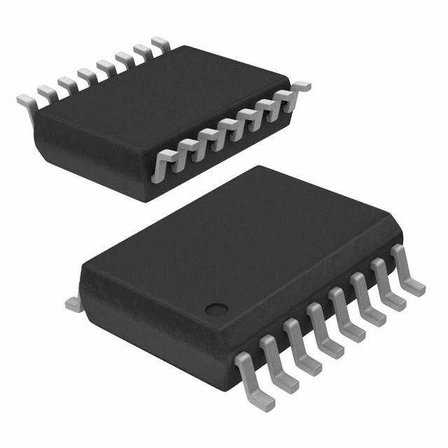
| 描述 | IC ADC 12BIT I2C 100KSPS 16WQFN模数转换器 - ADC 12B4-ch MUX input SAR ADC |
| 产品分类 | |
| 品牌 | Texas Instruments |
| 产品手册 | |
| 产品图片 |
|
| rohs | 符合RoHS无铅 / 符合限制有害物质指令(RoHS)规范要求 |
| 产品系列 | 数据转换器IC,模数转换器 - ADC,Texas Instruments ADS7924IRTERmicroPOWER™ |
| 数据手册 | 点击此处下载产品Datasheethttp://www.ti.com/lit/pdf/slyb174 |
| 产品型号 | ADS7924IRTER |
| 产品种类 | 模数转换器 - ADC |
| 位数 | 12 |
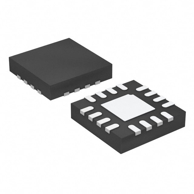
| 供应商器件封装 | 16-WQFN(3x3) |
| 其它名称 | 296-27456-6 |
| 分辨率 | 12 bit |
| 制造商产品页 | http://www.ti.com/general/docs/suppproductinfo.tsp?distId=10&orderablePartNumber=ADS7924IRTER |
| 包装 | Digi-Reel® |
| 商标 | Texas Instruments |
| 安装类型 | 表面贴装 |
| 安装风格 | SMD/SMT |
| 封装 | Reel |
| 封装/外壳 | 16-WFQFN 裸露焊盘 |
| 封装/箱体 | WQFN-16 |
| 工作温度 | -40°C ~ 85°C |
| 工作电源电压 | 2.2 V to 5.5 V |
| 工厂包装数量 | 3000 |
| 接口类型 | Serial I2C |
| 数据接口 | I²C, 串行 |
| 最大工作温度 | + 85 C |
| 最小工作温度 | - 40 C |
| 标准包装 | 1 |
| 特性 | - |
| 电压源 | 模拟和数字 |
| 系列 | ADS7924 |
| 结构 | SAR |
| 转换器数 | 1 |
| 转换速率 | 100 kS/s |
| 输入数和类型 | 4 个单端,单极 |
| 输入类型 | Single-Ended |
| 通道数量 | 4 Channel |
| 采样率(每秒) | 100k |


- 商务部:美国ITC正式对集成电路等产品启动337调查
- 曝三星4nm工艺存在良率问题 高通将骁龙8 Gen1或转产台积电
- 太阳诱电将投资9.5亿元在常州建新厂生产MLCC 预计2023年完工
- 英特尔发布欧洲新工厂建设计划 深化IDM 2.0 战略
- 台积电先进制程称霸业界 有大客户加持明年业绩稳了
- 达到5530亿美元!SIA预计今年全球半导体销售额将创下新高
- 英特尔拟将自动驾驶子公司Mobileye上市 估值或超500亿美元
- 三星加码芯片和SET,合并消费电子和移动部门,撤换高东真等 CEO
- 三星电子宣布重大人事变动 还合并消费电子和移动部门
- 海关总署:前11个月进口集成电路产品价值2.52万亿元 增长14.8%


PDF Datasheet 数据手册内容提取
Product Order Technical Tools & Support & Folder Now Documents Software Community ADS7924 SBAS482C–JANUARY2010–REVISEDSEPTEMBER2017 ADS7924 2.2 V, 12-Bit, 4-Channel, MicroPOWER 2 Analog-to-Digital Converter With I C Interface 1 Features 3 Description • IntelligentMonitoring: The ADS7924 is a four-channel, 12-bit, analog-to- 1 digital converter (ADC) with an I2C™ interface. With – Auto-Sequencingof4-ChannelMultiplexer its low-power ADC core, support for low-supply – IndividualAlarmThresholdsforEachChannel operation, and a flexible measurement sequencer – ProgrammableScanRate that essentially eliminates power consumption betweenconversions,theADS7924formsacomplete • MicroPOWER™Monitoring: monitoring system for power-critical applications such – Four-ChannelScanning: as battery-powered equipment and energy harvesting – Every1ms →25μW systems. – Every10ms→5 μW The ADS7924 features dedicated data registers and – < 1µAofPower-DownCurrent onboard programmable digital threshold comparators for each input. Alarm conditions can be programmed – ProgrammableInterruptPinControls that generate an interrupt. The combination of data Shutdown/WakeupoftheMicrocontroller buffering, programmable threshold comparisons, and – AutoPower-DownControl alarm interrupts minimize the host microcontroller – PWRCONPinAllowsShutdownofExternal timeneededtosupervisetheADS7924. OperationalAmplifiers The four-channel input multiplexer (MUX) is routed • WideSupplyRange: through external pins to allow a common signal conditioning circuit to be used between the MUX and – AnalogSupply:2.2Vto5.5V ADC, thereby reducing overall component count. The – DigitalSupply:1.65Vto5.5V low-power ADC uses the analog supply as its • SmallFootprint:3-mm× 3-mmWQFN reference and can acquire and convert signals in only 10 μs. An onboard oscillator eliminates the need to 2 Applications supplyamasterclock. • PortableandBattery-PoweredSystems: The ADS7924 is offered in a small 3-mm × 3-mm WQFN and is fully specified for operation over the – Medical,Communications,RemoteSensor industrialtemperaturerangeof –40°Cto85°C. SignalMonitoring,Power-SupplyMonitoring • EnergyHarvesting DeviceInformation(1) PARTNUMBER PACKAGE BODYSIZE(NOM) ADS7924 WQFN(16) 3.00mm×3.00mm (1) For all available packages, see the orderable addendum at theendofthedatasheet. SimplifiedSchematic MUX OUT ADCIN AVDD DVDD SDA I2C SCL CH0 Interface CH1 4-Channel SAR Data Buffers, A0 Sequencer, and CH2 MUX ADC Alarms INT CH3 PWRCON Oscillator RESET AGND DGND 1 An IMPORTANT NOTICE at the end of this data sheet addresses availability, warranty, changes, use in safety-critical applications, intellectualpropertymattersandotherimportantdisclaimers.PRODUCTIONDATA.
ADS7924 SBAS482C–JANUARY2010–REVISEDSEPTEMBER2017 www.ti.com Table of Contents 1 Features.................................................................. 1 7.4 DeviceFunctionalModes........................................13 2 Applications........................................................... 1 7.5 Programming...........................................................20 3 Description............................................................. 1 7.6 RegisterMap...........................................................26 4 RevisionHistory..................................................... 2 8 ApplicationandImplementation........................ 33 8.1 ApplicationInformation............................................33 5 PinConfigurationandFunctions......................... 3 8.2 TypicalApplication .................................................39 6 Specifications......................................................... 4 9 PowerSupplyRecommendations...................... 41 6.1 AbsoluteMaximumRatings......................................4 10 Layout................................................................... 41 6.2 ESDRatings..............................................................4 6.3 RecommendedOperatingConditions.......................4 10.1 LayoutGuidelines.................................................41 6.4 ThermalInformation..................................................4 10.2 LayoutExample....................................................41 6.5 ElectricalCharacteristics...........................................5 11 DeviceandDocumentationSupport................. 42 6.6 I2CTimingRequirements..........................................6 11.1 ReceivingNotificationofDocumentationUpdates42 6.7 TypicalCharacteristics..............................................7 11.2 CommunityResources..........................................42 7 DetailedDescription............................................ 10 11.3 Trademarks...........................................................42 7.1 Overview.................................................................10 11.4 ElectrostaticDischargeCaution............................42 7.2 FunctionalBlockDiagram.......................................10 11.5 Glossary................................................................42 7.3 FeatureDescription.................................................10 12 Mechanical,Packaging,andOrderable Information........................................................... 42 4 Revision History NOTE:Pagenumbersforpreviousrevisionsmaydifferfrompagenumbersinthecurrentversion. ChangesfromRevisionB(September2015)toRevisionC Page • ChangedQFNtoWQFNthroughoutdocument .................................................................................................................... 1 • ChangeddirectionofRESETarrowinSimplifiedSchematicfigure....................................................................................... 1 • ChangedmaximumoperatingtemperaturerangeinAbsoluteMaximumRatingstable........................................................ 4 • ChangeddirectionofRESETarrowinFunctionalBlockDiagramfigure ............................................................................ 10 • Changeddescriptionofbits7:5inINTCONFIG:InterruptConfigurationRegister .............................................................. 30 ChangesfromRevisionA(May2010)toRevisionB Page • AddedESDRatingstable,FeatureDescriptionsection,DeviceFunctionalModes,ApplicationandImplementation section,PowerSupplyRecommendationssection,Layoutsection,DeviceandDocumentationSupportsection,and Mechanical,Packaging,andOrderableInformationsection ................................................................................................. 1 2 SubmitDocumentationFeedback Copyright©2010–2017,TexasInstrumentsIncorporated ProductFolderLinks:ADS7924
ADS7924 www.ti.com SBAS482C–JANUARY2010–REVISEDSEPTEMBER2017 5 Pin Configuration and Functions RTEPackage 16-PinWQFN TopView T U DD DD CIN XO V V D U D A A M 6 5 4 3 1 1 1 1 RESET 1 12 CH0 INT 2 Thermal 11 CH1 SCLK 3 Pad(1) 10 CH2 SDA 4 9 CH3 5 6 7 8 0 D N D A N O N G C G D R A W P (1) ConnecttoAGND. PinFunctions PIN I/O DESCRIPTION NO. NAME 1 RESET Digitalinput Externalreset,activelow 2 INT Digitaloutput Interruptpin,activelow;generatedwheninputvoltageisbeyondprogrammedthreshold 3 SCLK Digitalinput Serialclockinput Digital 4 SDA Serialdata input/output 5 A0 Digitalinput I2Caddressselection 6 DGND Digital Digitalground 7 PWRCON Digitaloutput Powercontrolpintocontrolshutdown/power-upofexternaloperationalamplifier 8 AGND Analog Analogground 9 CH3 Analoginput Inputchannel3 10 CH2 Analoginput Inputchannel2 11 CH1 Analoginput Inputchannel1 12 CH0 Analoginput Inputchannel0 13 MUXOUT Analogoutput Multiplexeroutput 14 ADCIN Analoginput ADCinput 15 AVDD Analog Analogsupply 16 DVDD Digital Digitalsupply Copyright©2010–2017,TexasInstrumentsIncorporated SubmitDocumentationFeedback 3 ProductFolderLinks:ADS7924
ADS7924 SBAS482C–JANUARY2010–REVISEDSEPTEMBER2017 www.ti.com 6 Specifications 6.1 Absolute Maximum Ratings Overoperatingfree-airtemperaturerange,unlessotherwisenoted.(1) MIN MAX UNIT Supplyvoltage,AVDDtoAGND –0.3 6 V Supplyvoltage,DVDDtoDGND –0.3 6 V Supplyvoltage,DVDDtoAVDD AVDD≥DVDD V AGNDtoDGND –0.3 0.3 V Analoginputvoltage AGND–0.3 0.3 V DigitalinputvoltagewithrespecttoDGND(SCLandSDA) DGND–0.3 6 V DigitalinputvoltagewithrespecttoDGND(A0,RESET) DGND–0.3 DVDD+0.3 V Inputcurrenttoallpinsexceptsupplypins –10 10 mA Maximumoperatingtemperature –40 85 °C Storagetemperature –60 150 °C (1) StressesbeyondthoselistedunderAbsoluteMaximumRatingsmaycausepermanentdamagetothedevice.Thesearestressratings only,whichdonotimplyfunctionaloperationofthedeviceattheseoranyotherconditionsbeyondthoseindicatedunderRecommended OperatingConditions.Exposuretoabsolute-maximum-ratedconditionsforextendedperiodsmayaffectdevicereliability. 6.2 ESD Ratings VALUE UNIT Human-bodymodel(HBM),perANSI/ESDA/JEDECJS-001(1) ±2000 V(ESD) Electrostaticdischarge Charged-devicemodel(CDM),perJEDECspecificationJESD22- V C101(2) ±750 (1) JEDECdocumentJEP155statesthat500-VHBMallowssafemanufacturingwithastandardESDcontrolprocess. (2) JEDECdocumentJEP157statesthat250-VCDMallowssafemanufacturingwithastandardESDcontrolprocess. 6.3 Recommended Operating Conditions overoperatingfree-airtemperaturerange(unlessotherwisenoted) MIN NOM MAX UNIT AVDD AnalogSupplyVoltage 2.2 5.5 V DVDD DigitalSupplyVoltage 1.65 AVDD V 6.4 Thermal Information ADS7924 THERMALMETRIC(1) RTE(WQFN) UNIT 16PINS R Junction-to-ambientthermalresistance 48.1 °C/W θJA R Junction-to-case(top)thermalresistance 47.3 °C/W θJC(top) R Junction-to-boardthermalresistance 60.8 °C/W θJB ψ Junction-to-topcharacterizationparameter 0.3 °C/W JT ψ Junction-to-boardcharacterizationparameter 14.1 °C/W JB R Junction-to-case(bottom)thermalresistance 0.4 °C/W θJC(bot) (1) Formoreinformationabouttraditionalandnewthermalmetrics,seetheSemiconductorandICPackageThermalMetricsapplication report. 4 SubmitDocumentationFeedback Copyright©2010–2017,TexasInstrumentsIncorporated ProductFolderLinks:ADS7924
ADS7924 www.ti.com SBAS482C–JANUARY2010–REVISEDSEPTEMBER2017 6.5 Electrical Characteristics MinimumandmaximumspecificationsareatT =–40°Cto85°C,1.65V<DVDD<5.5V,and2.2V<AVDD<5.5V. A TypicalspecificationsareatT =25°C,AVDD=5V,andDVDD=5V,unlessotherwisenoted. A PARAMETER TESTCONDITIONS MIN TYP MAX UNIT ANALOGINPUT Full-scaleinputspan (CHX–AGND) 0 AVDD V Inputcapacitance(1) 4 10 pF ADCsamplingcapacitance 15 pF MUXresistance 60 Ω Inputchannelcrosstalk 85 dB SYSTEMPERFORMANCE Resolution 12 Bits Nomissingcodes 12 Bits Integrallinearity –1.5 ±0.5 1.5 LSBs Differentiallinearity –1 ±0.6 1.5 LSBs Offseterror –5 5 LSBs Offseterrordrift 0.01 LSB/°C Gainerror –0.2% –0.01% 0.2% Gainerrordrift 0.6 ppm/°C Noise(rms) 0.125 LSB SAMPLINGDYNAMICS Monitoringtime/channel(2) 10 µs CLOCK Internalclockfrequencyvariation ±20% DIGITALINPUT/OUTPUT Logicfamily CMOS Logiclevel: VIH(SDA,SCL,A0,RESET) 0.8DVDD DVDD+0.3 V VIL(SDA,SCL,A0,RESET) DGND–0.3 0.4 V Inputcurrent II VI=DVDDorDGND –10 10 μA IOH=100μA,INTpin 0.8DVDD DVDD V VOH(PWRCON,INT) IOH=100µA,PWRCONpin 0.8AVDD AVDD V VOL(PWRCON,INT,SDA) IOL=100μA DGND 0.4 V Low-leveloutputcurrent IOL SDApin,VOL=0.6V 3 mA Loadcapacitance CB SDApin 400 pF Dataformat Straightbinary POWER-SUPPLYREQUIREMENTS Power-supplyvoltage: DVDD(3) 1.65 5.5 V AVDD 2.2 5.5 V IAVDD(4) tCYCLE=2.5ms,AVDD=2.2V 5 8 μA IPWRD,power-downcurrent <1 μA TEMPERATURERANGE Specifiedperformance –40 85 °C (1) CH0toCH3inputpincapacitance. (2) Rateatwhichchannelscanbescanned.Thisistheminimumacquisitiontime(6µs)andconversiontime(4µs). (3) DVDDcannotexceedAVDD. (4) SeeFigure3andFigure4formoreinformation. Copyright©2010–2017,TexasInstrumentsIncorporated SubmitDocumentationFeedback 5 ProductFolderLinks:ADS7924
ADS7924 SBAS482C–JANUARY2010–REVISEDSEPTEMBER2017 www.ti.com 6.6 I2C Timing Requirements MIN MAX UNIT f SCLoperatingfrequency 0 0.4 MHz SCL t BusfreetimebetweenSTARTandSTOPcondition 1.3 μs BUF HoldtimeafterrepeatedSTARTcondition. t 600 ns HDSTA Afterthisperiod,thefirstclockisgenerated. t RepeatedSTARTconditionsetuptime 600 ns SUSTA t Stopconditionsetuptime 600 ns SUSTO t Dataholdtime 0 ns HDDAT t Datasetuptime 100 ns SUDAT t SCLclocklowperiod 1300 ns LOW t SCLclockhighperiod 600 ns HIGH t Clock/datafalltime 300 ns F t Clock/datarisetime 300 ns R t Datavalidtime 0.9 μs VDDAT t Datavalidacknowledgetime 0.9 μs VDACK t Pulsewidthofspikethatmustbesuppressedbytheinputfilter 0 50 ns SP t VDDAT t HIGH tR tVDACK t tHDSTA F t SCL LOW tHDSTA tSUDAT 9th Clock tSUSTA tSUSTO t t SP HDDAT SDA t BUF P S Sr P NOTE:S=Start,Sr=RepeatedStart,andP=Stop. Figure1. I2CTimingDiagram 6 SubmitDocumentationFeedback Copyright©2010–2017,TexasInstrumentsIncorporated ProductFolderLinks:ADS7924
ADS7924 www.ti.com SBAS482C–JANUARY2010–REVISEDSEPTEMBER2017 6.7 Typical Characteristics AtT =25°C,unlessotherwisenoted. A 14 1000 Auto-Single Mode AVDD = 2.2V 12 tCYCLE= 2.5ms tPU= 0V AVDD = DVDD= 5.0V t = 6ms ACQ 10 Fast I2C Interface Mode 100 A) W) ment ( 8 mer ( (4-ChAauntnoe-Sl cMaena Msuordeemsents) urr 6 ow C Analog Current P 10 4 Auto-Single Modes 2 Digital Current (1-Channel Measurements) 0 1 -40.0 -25.5 -11.0 3.5 18.0 32.5 47.0 61.5 76.0 90.5 105.0 0.01 0.1 1 10 100 1000 Temperature (°C) t (ms) CYCLE Figure2.CurrentvsTemperature Figure3.AveragePowerDissipationvsCycleTime 10000 10 AVDD = 5V Auto-Single Mode t = 0V 9 t = 2.5ms PU CYCLE t = 6ms A) 8 1000 ACQ mnt ( 7 e W) Auto-Scan Modes urr 6 m (4-Channel Measurements) C wer ( 100 pply 5 o u 4 P S 10 Auto-Single Modes alog 3 (1-Channel Measurements) An 2 1 1 0 0.01 0.1 1 10 100 1000 2.0 2.5 3.0 3.5 4.0 4.5 5.0 5.5 6.0 t (ms) AVDD Supply Voltage (V) CYCLE Figure4.AveragePowerDissipationvsCycleTime Figure5.AnalogSupplyCurrentvsSupplyVoltage 0 0 30 Units Across Two Lots AVDD = 2.2V -1 -1 -2 -2 B) -3 B) -3 LS -4 LS -4 Error ( -5 Error ( -5 n -6 n -6 ai ai G -7 G -7 -8 Mean +s -8 Mean -9 Mean-s -9 -10 -10 2 3 4 5 6 -40.0 -25.5 -11.0 3.5 18.0 32.5 47.0 61.5 76.0 90.5 105.0 AVDD Supply Voltage (V) Temperature (°C) Figure6.TypicalGainErrorvsAVDDVoltage Figure7.GainErrorDrift Copyright©2010–2017,TexasInstrumentsIncorporated SubmitDocumentationFeedback 7 ProductFolderLinks:ADS7924
ADS7924 SBAS482C–JANUARY2010–REVISEDSEPTEMBER2017 www.ti.com Typical Characteristics (continued) AtT =25°C,unlessotherwisenoted. A 3 5.0 30 Units Across Two Lots AVDD = 2.2V 4.5 2 4.0 SB) 1 SB) 3.5 MMeeaann +s Error (L 0 Error (L 32..05 Mean-s et et 2.0 Offs -1 Offs 1.5 -2 1.0 0.5 -3 0 -40 -11 18 47 76 105 2 3 4 5 6 Temperature (°C) AVDD Voltage (V) Figure8.OffsetErrorDrift,Typical Figure9.TypicalOffsetErrorvsAVDDVoltage 1.5 2.0 AVDD = 2.2V 1.4 1.5 al) 1.3 min 1.2 B) 1.0 of No 1.1 or (LS 0.5 % 1.0 Err 0 ncy ( 0.9 arity -0.5 e e u 0.8 n eq Li -1.0 Fr 0.7 0.6 -1.5 0.5 -2.0 2 3 4 5 6 0 512 1024 1536 2048 2560 3072 3584 4096 AVDD Voltage (V) Code Figure10.InternalOscillatorFrequencyvsVoltage Figure11.IntegralNonlinearity 2.0 2.0 AVDD = 5.0V AVDD = 2.2V 1.5 1.5 B) 1.0 1.0 S Maximum INL or (L 0.5 SB) 0.5 earity Err -0.05 INL (L -0.05 Minimum INL n Li -1.0 -1.0 -1.5 -1.5 INL shown is worst result over transfer function. -2.0 -2.0 0 512 1024 1536 2048 2560 3072 3584 4096 -40.0 -25.5 -11.0 3.5 18.0 32.5 47.0 61.5 76.0 90.5 105.0 Code Temperature (°C) Figure12.IntegralNonlinearity Figure13.IntegralLinearityErrorDrift 8 SubmitDocumentationFeedback Copyright©2010–2017,TexasInstrumentsIncorporated ProductFolderLinks:ADS7924
ADS7924 www.ti.com SBAS482C–JANUARY2010–REVISEDSEPTEMBER2017 Typical Characteristics (continued) AtT =25°C,unlessotherwisenoted. A 1.5 1.5 AVDD = 5V AVDD = 2.2V 1.0 1.0 B) B) S 0.5 S 0.5 L L or ( or ( Err 0 Err 0 y y earit -0.5 earit -0.5 n n Li Li -1.0 -1.0 -1.5 -1.5 0 512 1024 1536 2048 2560 3072 3584 4096 0 512 1024 1536 2048 2560 3072 3584 4096 Code Code Figure14.DifferentialNonlinearity Figure15.DifferentialNonlinearity 1.5 9000 AVDD = 2.2V DC Input 8000 AVDD = 2.2V 1.0 7000 0.5 6000 B) Maximum DNL L (LS 0 ount 5000 N C 4000 D Minimum DNL -0.5 3000 -1.0 2000 DNL shown is worst result over transfer function. 1000 -1.5 0 -40.0 -25.5 -11.0 3.5 18.0 32.5 47.0 61.5 76.0 90.5 105.0 3 4 5 6 7 8 9 0 1 2 3 Temperature (°C) 04 04 04 04 04 04 04 05 05 05 05 2 2 2 2 2 2 2 2 2 2 2 Code Atcodecenter Figure16.DifferentialNonlinearityvsTemperature Figure17.NoiseHistogram (1) 9000 DC Input 8000 AVDD = 5V 7000 6000 nt 5000 u o C 4000 3000 2000 1000 0 3 4 5 6 7 8 9 0 1 2 3 4 4 4 4 4 4 4 5 5 5 5 0 0 0 0 0 0 0 0 0 0 0 2 2 2 2 2 2 2 2 2 2 2 Code Atcodecenter Figure18.NoiseHistogram (1) Atcodecenter. Copyright©2010–2017,TexasInstrumentsIncorporated SubmitDocumentationFeedback 9 ProductFolderLinks:ADS7924
ADS7924 SBAS482C–JANUARY2010–REVISEDSEPTEMBER2017 www.ti.com 7 Detailed Description 7.1 Overview The ADS7924 is a miniature, four-channel, multiplexed, 12-bit, analog-to-digital converter (ADC) with an I2C serial interface. Functional Block Diagram shows a block diagram. The four-channel input multiplexer is routed through external pins to allow a common signal conditioning block to be used for all four channels. The PWRCON digital output can be used to shut down active circuitry used in the signal conditioning; see the ApplicationandImplementationsectionforadditionaldetails. The successive-approximation-register (SAR) ADC performs a no-latency conversion on the selected input channel and stores the data in a dedicated register. A digital threshold comparator with programmable upper and lower limits can be enabled and used to create an alarm monitor. A dedicated interrupt output pin (INT) indicates when an alarm occurs. Two I2C addresses are available and are selected with the dedicated digital input pin A0. BothstandardandfastmodeformatsforI2Caresupported. 7.2 Functional Block Diagram MUX OUT ADCIN AVDD DVDD Registers RESET CH0 Upper Limit Control CH1 Upper Limit and PWRCON Sequencer CH2 Upper Limit I2C SDA CH3 Upper Limit Interface SCL CH0 CH0 Data A0 CH1 Input SAR CH1 Data CH2 Multiplexer ADC CH2 Data INT CH3 CH3 Data Comparator and Alarm Detect CH0 Lower Limit CH1 Lower Limit CH2 Lower Limit CH3 Lower Limit Clock Oscillator AGND AGND 7.3 Feature Description 7.3.1 Multiplexer The ADS7924 has a four-channel, single-ended input multiplexer. As Figure 19 illustrates, ESD diodes protect the inputs. Make sure these diodes do not turn on by staying within the absolute input voltage range specification. The MUXOUT pin can be connected to AGND within the multiplexer (for example, to provide a test signal of 0 V or as part of a calibration procedure). See the PWRCONFIG: Power-Up Configuration Register registerintheRegisterMapsectionformoredetails 10 SubmitDocumentationFeedback Copyright©2010–2017,TexasInstrumentsIncorporated ProductFolderLinks:ADS7924
ADS7924 www.ti.com SBAS482C–JANUARY2010–REVISEDSEPTEMBER2017 Feature Description (continued) MUXOUT AVDD CH0 AVDD AGND CH1 AVDD AGND CH2 AVDD AGND CH3 (1) AGND AGND (1) SeethePWRCONFIG:Power-UpConfigurationRegisterregisterintheRegisterMapsection. Figure19. ADS7924Multiplexer 7.3.2 ADCInput The ADC Input (ADCIN) pin provides a single-ended input to the 12-bit successive approximation register (SAR) ADC. This pin is protected with ESD diodes in the same way as the multiplexer inputs. While acquiring the signal during the t interval, the ADC sampling capacitor is connected to the ADCIN pin. While converting during the ACQ t interval, the sampling capacitor is disconnected from the ADCIN pin, and the conversion process CONV determinesthevoltagethatwassampled. 7.3.3 Reference The analog supply voltage (AVDD) is used as the reference. Power to the ADS7924 should be clean and well bypassed.A0.1-μFceramiccapacitormustbeplacedascloseaspossibletotheADS7924package.Inaddition, a1-μFto10-μFcapacitoranda5-Ω to10-Ωseriesresistormaybeusedtolow-passfilteranoisysupply. 7.3.4 Clock TheADS7924usesaninternalclock.Theclockspeeddeterminesthevarioustimingsettingssuchasconversion time,acquisitiontime,andsoforth. 7.3.5 DataFormat TheADS7924provides12bitsofdatainunipolarformat.Thepositivefull-scaleinputproducesanoutputcodeof FFFh and a zero input produces an output code of 0h. The output clips at these codes for signals that either exceedfull-scaleorgobelow'0'.Figure20illustratescodetransitionsversusinputvoltage. Copyright©2010–2017,TexasInstrumentsIncorporated SubmitDocumentationFeedback 11 ProductFolderLinks:ADS7924
ADS7924 SBAS482C–JANUARY2010–REVISEDSEPTEMBER2017 www.ti.com Feature Description (continued) FFF FFE x) ¼ e H e ( 800 d o C ut 7FE p ut ¼ O 001 1LSB = AVDD/212 000 ¼ 0 0.5LSB AVDD-1.5LSB AVDD Input Voltage (V ) ACDIN (1) Excludestheeffectsofnoise,INL,offset,andgainerrors. Figure20. ADS7924CodeTransitionDiagram(1) 7.3.6 ADCConversionTiming The ADS7924 provides a flexible timing arrangement to support a wide variety of measurement needs. Three user-controlled timings include power up (t ), acquisition (t ), and sleep (t ) plus a fixed conversion time PU ACQ SLEEP (t ). CONV 7.3.6.1 Power-UpTime The power-up time is allowed to elapse whenever the device has been shutdown in idle mode. Power-up time can allow external circuits, such as an operational amplifier, between the MUXOUT and ADCIN pins to turn on. ThenominaltimeprogrammedbythePUTIME[4:0]registerbitsisgivenbyEquation1: t =PWRUPTIME[4:0]×2μs (1) PU For example, if PWRUPTIME is set to 25 ('011001') then 50 μs is allowed to elapse before beginning the acquisitiontime.Ifapower-uptimeisnotrequired,setthebitsto'0'toeffectivelybypass. 7.3.6.2 AcquisitionTime The acquisition time is allowed to elapse before beginning a conversion. During this time, the ADC acquires the signal.Theminimumacquisitiontimeis6µs.ThenominaltimeprogrammedbytheACQTIME[4:0]registerbitsis givenbyEquation2: t =(ACQTIME[4:0]×2μs)+6μs (2) ACQ For example, if ACQTIME is set to 30 ('011110') then 66 μs is allowed to acquire the input signal. If an acquisitiontimegreaterthan6 μsisnotrequired,setthebitsto'0'. 7.3.6.3 ConversionTime Theconversiontimeisalways4 μsandcannotbeprogrammedbytheuser. 7.3.6.4 SleepTime The sleep time is allowed to elapse after conversions in the Auto-Single with Sleep, Auto-Scan with Sleep, and Auto-Burst Scan with Sleep modes. The nominal time programmed by the SLPTIME registers can be increased byafactorofeightusingtheSLPMULT8bitordecreasedbyafactoroffourusingtheSLPDIV4bit. 7.3.7 InterruptOutput(INT) The ADS7924 offers a dedicated output pin (INT) for signaling an interrupt condition. The INT pin can be configured to activate when the ADC is busy with a conversion, when data are ready for retrieval, or when an alarm condition occurs; see the INTCONFIG: Interrupt Configuration Register register in the Register Map section. 12 SubmitDocumentationFeedback Copyright©2010–2017,TexasInstrumentsIncorporated ProductFolderLinks:ADS7924
ADS7924 www.ti.com SBAS482C–JANUARY2010–REVISEDSEPTEMBER2017 Feature Description (continued) Toclearaninterruptfromanalarmcondition,readtheINTCONFIGregister(12h).Toclearaninterruptfromdata ready,readthedataregisters.Theinterruptclearswhenthelowerfourbitsareretrieved. The INT pin can be configured to generate a static output (useful for a host controller monitoring for a level) or a pulse output (useful for a host controller monitoring for a edge transition). When a pulse output is selected, the nominalpulsewidthis250ns.TheInterruptControlRegistershouldbereadtocleartheinterrupt. 7.3.8 PWRCON The PWRCON pin allows the user to synchronize the shutdown/wakeup of an external operational amplifier with the ADC conversion cycle. This feature provides further power reduction and can be useful in applications where the time difference between consecutive signal captures is large. The PWRCON pin can drive up to 3 mA of currentanditsoutputvoltageisthesameasAVDD.ThispiniscontrolledbythePWRCONFIGregister. 7.3.9 Alarm The ADS7924 offers an independent alarm function for each input channel. An 8-bit window comparator can be enabled to test the ADC conversion result against an upper limit set by the ULR register and against a lower limit setbytheLLRregister.IftheconversionresultislessthanorequaltotheLLRthresholdvalueorgreaterthanor equal to the ULR threshold value, the comparator is tripped. There are separate upper and lower registers for eachinputchannel. A programmable counter determines how many comparator trips it takes to generate an alarm. A separate counter is used for each channel and is incremented whenever the comparator trips, either for the upper or lower thresholds. That is, an ADC conversion result on channel 1 that exceeds the ULR threshold or falls below the LLR threshold increments the counter for that channel. Figure 21 illustrates a conceptual diagram of the window comparatorandalarmcircuitry. When an alarm occurs, the INT pin can be configured to generate an interrupt. The channel that generated the alarm can be read from the registers. A read of the Interrupt Control register clears the alarm register and also resetsthealarmcounter. 7.4 Device Functional Modes 7.4.1 ADCOperatingModes The ADS7924 offers multiple operating modes to support a variety of monitoring needs. Conversions can either be started manually or set to automatically continue. The mode is set by writing to the MODE register, and changestakeeffectassoonasthewritecompletes.Table1givesabriefdescriptionofeachmode. 7.4.1.1 IdleMode Usethismodetosavepowerwhennotconverting.Allcircuitsareshutdown. 7.4.1.2 AwakeMode All circuits are operating in this mode and the ADC is ready to convert. When switching between modes, be sure to first select the Awake mode and then switch to the desired mode. This procedure ensures the internal control logicisproperlysynchronized. Copyright©2010–2017,TexasInstrumentsIncorporated SubmitDocumentationFeedback 13 ProductFolderLinks:ADS7924
ADS7924 SBAS482C–JANUARY2010–REVISEDSEPTEMBER2017 www.ti.com Device Functional Modes (continued) Upper Limit Threshold ALMCNT[2:0](1) ULRx[7:0](2) Window ADC CHX Data Comparator Counter X Alarm for X(2) Channel X LLRx[7:0] Lower Limit Threshold (1) ThesameALMCNTvalueisusedforallfourwindowcomparators. (2) X=0to3. Figure21. WindowComparatorandAlarmConceptualBlockDiagram Table1.ModeDescriptions MODE DESCRIPTION Idle Allcircuitsshutdown;lowestpowersetting Awake Allcircuitsawakeandreadytoconvert Manual-Single Selectinputchannelisconvertedonce Manual-Scan Allinputchannelsareconvertedonce Auto-Single Oneinputchanneliscontinuouslyconverted Auto-Scan Allinputchannelsarecontinuouslyconverted Auto-SinglewithSleep Oneinputchanneliscontinuouslyconvertedwithprogrammablesleeptimebetweenconversions Auto-ScanwithSleep Allinputchannelsarecontinuouslyconvertedwithprogrammablesleeptimebetweenconversions Auto-BurstScanwith Allinputchannelsareconvertedwithminimaldelayfollowedbyaprogrammablesleeptime Sleep 7.4.1.3 Manual-SingleMode This mode converts the selected channel once; see Figure 22. After the ADC Mode Control register is written, the power-up time (t ) and acquisition time (t ) are allowed to elapse. t can be set to '0' to effectively PU ACQ PU bypass if not needed. t time is programmable through the ACQCONFIG register, bits[4:0]. Sleep time (t ) ACQ SLEEP isnotusedinthismode. After the conversion completes, the device waits for a new mode to be set. This mode can be set to Idle to save power. When t and t are very short, the very short conversion time needed allows a read register operation PU ACQ tobeissuedontheI2Cbusimmediatelyafterthewriteoperationthatinitiatesthismode. NOTE t onlyappliestothefirstmanual-singlecommand. PU If multiple conversions are needed, the manual-single mode can be reissued without requiring the awake mode tobeissuedinbetween.Consecutivemanual-singlecommandshavenot period. PU 14 SubmitDocumentationFeedback Copyright©2010–2017,TexasInstrumentsIncorporated ProductFolderLinks:ADS7924
ADS7924 www.ti.com SBAS482C–JANUARY2010–REVISEDSEPTEMBER2017 Acquire Convert Awaiting Status Awake Selected Selected Mode Channel Channel Selection t t t PU ACQ CONV InputMultiplexer Selected Channel Busy(1) Data Ready(1) PWRCON(2) (3) (1) Busy and data ready are internal signals shown as active high that can be routed to the INT pin for external monitoring. (2) PWRCONisshownenabledandactivehigh. (3) ThemodebeginsonthetrailingedgeoftheI2CacknowledgeafterwritingtotheMODECNTLregister. Figure22. Manual-SingleOperationExample 7.4.1.4 Manual-ScanMode This mode converts all of the channels once, starting with the selected channel, as illustrated in Figure 23. After the ADC Mode Control register is written, the power-up time (t ) is allowed to elapse. This value can be set to PU '0' to effectively bypass if not needed. Before each conversion, an acquisition time (t ) is allowed to elapse. ACQ t time is programmable through the ACQCONFIG register, bits[4:0]. Sleep time (t ) is not used in this ACK SLEEP mode. The input multiplexer is automatically incremented as the conversions complete. If, for example, the initial selected channel is CH2, the conversion order is CH2, CH3, CH0, and CH1. Data from the conversions are always put into the data register that corresponds to a particular channel. For example, CH2 data always goes in register DATA2_H and DATA2_L regardless of conversion order. After all four conversions complete, the device waits for a new mode to be set. This mode can be set to Idle afterwards to save power. The INT pin can be configured to indicate the completion of each individual conversion or it can wait until all four finish. In either case, the appropriate data register is updated after each conversion. These registers can be read at any time afterwards. If multiple scan are needed, the manual-scan mode can be reissued without requiring the Awake modetobeissuedinbetween. Copyright©2010–2017,TexasInstrumentsIncorporated SubmitDocumentationFeedback 15 ProductFolderLinks:ADS7924
ADS7924 SBAS482C–JANUARY2010–REVISEDSEPTEMBER2017 www.ti.com Acquire Convert Acquire Convert Acquire Convert Acquire Convert Awaiting Status Awake First First Second Second Third Third Fourth Fourth Mode Channel Channel Channel Channel Channel Channel Channel Channel Selection t t t t t t t t t PU ACQ CONV ACQ CONV ACQ CONV ACQ CONV InputMultiplexer Selected Channel Next Channel Next Channel Next Channel Busy(1) Data Ready(2) PWRCON(3) (4) (1) BusyisaninternalsignalshownasactivehighthatcanberoutedtotheINTpinforexternalmonitoring. (2) Data ready is an internal signal shown as active high and is enabled when all conversions are complete. It can be routedtotheINTpinforexternalmonitoring. (3) PWRCONisshownenabledandactivehigh. (4) ThemodebeginsonthetrailingedgeoftheI2CacknowledgeafterwritingtotheMODECNTLregister. Figure23. Manual-ScanOperationExample 7.4.1.5 Auto-SingleMode This mode automatically converts the selected channel continuously; see Figure 24. After the ADC Mode Control register is written, the power-up time (t ) is allowed to elapse. This value can be set to '0' to effectively bypass if PU not needed. Before the conversion, an acquisition time (t ) is allowed to elapse. t time is programmable ACQ ACQ through the ACQCONFIG register, bits[4:0]. Sleep time (t ) is not used in this mode. After the conversion SLEEP completesthecycleisrepeated. This mode can be used with the onboard digital comparator to monitor the status of an input signal with little support needed from a host microcontroller. The conversion time is less than the I2C data retrieval time. TI suggests stopping this mode by setting the mode to Idle or stopping the conversion by configuring the alarm to doso,beforeretrievingdata.Thealarmcanalsobeconfiguredtocontinuetheconversionevenafteraninterrupt isgenerated. 16 SubmitDocumentationFeedback Copyright©2010–2017,TexasInstrumentsIncorporated ProductFolderLinks:ADS7924
ADS7924 www.ti.com SBAS482C–JANUARY2010–REVISEDSEPTEMBER2017 Acquire Convert Acquire Convert Acquire Convert S tatus Awake Selected Selected Selected Selected Selected Selected Channel Channel Channel Channel Channel Channel t t t t t t t PU ACQ CONV ACQ CONV ACQ CONV InputMultiplexer Selected Channel(1) Busy(2) PWRCON(3) (4) (1) Samechanneliscontinuouslyconverted. (2) BusyisaninternalsignalshownasactivehighthatcanberoutedtotheINTpinforexternalmonitoring. (3) PWRCONisshownenabledandactivehigh. (4) ThemodebeginsonthetrailingedgeoftheI2CacknowledgeafterwritingtotheMODECNTLregister. Figure24. ExampleofAuto-SingleOperation 7.4.1.6 Auto-ScanMode This mode automatically converts all the channels continuously, starting with the selected channel, as shown in Figure25.AftertheADCModeControlregisteriswritten,thepower-uptime(t )isallowedtoelapse.Thisvalue PU canbesetto'0'toeffectivelybypassifnotneeded.Beforetheconversion,anacquisitiontime(t )isallowedto ACQ elapse. t time is programmable through the ACQCONFIG register, bits[4:0]. Sleep time (t ) is not used in ACQ SLEEP this mode. The input multiplexer is automatically incremented as the conversions complete. If, for example, the initial selected channel is CH2, the conversion order is CH2, CH3, CH0, CH1, CH2, CH3, and so forth. until the mode is stopped. Data from the conversions are always put into the data register that corresponds to a particular channel.Forexample,CH2dataalwaysgoinregisterDATA2_HandDATA2_Lregardlessofconversionorder. This mode can be used with the onboard digital comparator to monitor the status of the input signals with little support needed from a host microcontroller. TI suggests interrupting this mode and stopping the automatic conversions,eitherbysettingthemodetoIdleorconfiguringthealarmtodoso,beforeretrievingdata. Acquire Convert Acquire Convert Acquire Convert Acquire Convert Acquire Convert Status Awake First First Second Second Third Third Fourth Fourth First First Channel Channel Channel Channel Channel Channel Channel Channel Channel Channel t t t t t t t t t t t PU ACQ CONV ACQ CONV ACQ CONV ACQ CONV ACQ CONV Input Multiplexer Selected Channel (First) Next Channel Next Channel Next Channel First Channel Busy(1) PWRCON(2) (3) (1) BusyisaninternalsignalshownasactivehighthatcanberoutedtotheINTpinforexternalmonitoring. (2) PWRCONisshownenabledandactivehigh. (3) ThemodebeginsonthetrailingedgeoftheI2CacknowledgeafterwritingtotheMODECNTLregister. Figure25. Auto-ScanOperationExample Copyright©2010–2017,TexasInstrumentsIncorporated SubmitDocumentationFeedback 17 ProductFolderLinks:ADS7924
ADS7924 SBAS482C–JANUARY2010–REVISEDSEPTEMBER2017 www.ti.com 7.4.1.7 Auto-SingleWithSleepMode This mode automatically converts the selected channel repeatedly with a sleep interval between conversions, as shown in Figure 26. After the ADC Mode Control register is written, the power-up time (t ) is allowed to elapse. PU This value can be set to '0' to effectively bypass if not needed. Before the conversion, an acquisition time (t ) ACQ isallowedtoelapse.t timeisprogrammablethroughtheACQCONFIGregister,bits[4:0].Aftertheconversion, ACQ sleep time (t ) is allowed to elapse and then the cycle repeats. The length of the sleep time is controlled by SLEEP registerbits.Duringthesleepmode,powerdissipationisminimalandthePWRCONoutputisalwaysdisabled. This mode can be used with the onboard digital comparator to periodically monitor the status of an input signal while saving power between conversions. Little support is needed from a host microcontroller. It is suggested to stop this mode by setting the mode to Idle or stopping the conversion by configuring the alarm to do so, before retrieving data. The length in time of the cycle (t ) sets the average power dissipation; see Figure 3 or CYCLE Figure4. t CYCLE Acquire Convert Acquire Convert Acquire Convert S tatus Awake Selected Selected Sleep Awake Selected Selected Sleep Awake Selected Selected Channel Channel Channel Channel Channel Channel t t t PU PU PU t t t t t t t t ACQ CONV SLEEP ACQ CONV SLEEP ACQ CONV InputMultiplexer Selected Channel(1) Busy(2) PWRCON(3) (4) (1) Samechanneliscontinuouslyconverted. (2) BusyisaninternalsignalshownasactivehighthatcanberoutedtotheINTpinforexternalmonitoring. (3) PWRCONisshownenabledandactivehigh. (4) ThemodebeginsonthetrailingedgeoftheI2CacknowledgeafterwritingtotheMODECNTLregister. Figure26. Auto-SingleWithSleepOperationExample 7.4.1.8 Auto-ScanWithSleepMode This mode automatically converts all the channels repeatedly with a sleep interval between conversions, as illustrated in Figure 27. After the ADC Mode Control register is written, the power-up time (t ) is allowed to PU elapse. This value can be set to '0' to effectively bypass if not needed. Before the first conversion of the selected input, an acquisition time (t ) is allowed to elapse. t time is programmable through the ACQCONFIG ACQ ACQ register, bits[4:0]. After the conversion, a sleep time (t ) is allowed to elapse and then the cycle repeats. The SLEEP lengthofthesleeptimeiscontrolledbyregisterbits.Duringthesleepmode,powerdissipationisminimalandthe PWRCON output is always disabled. The input multiplexer is automatically incremented as the conversions complete.If,forexample,theinitialselectedchannelisCH2,theconversionorderisCH2,CH3,CH0,CH1,CH2, CH3, and so forth until the mode is stopped. Data from the conversions are always put into the data register that corresponds to a particular channel. For example, CH2 data always goes in register DATA2_H and DATA2_L regardlessofconversionorder. This mode can be used with the onboard digital comparator to periodically monitor the status of the input signals while saving power between conversions. Little support is needed from a host microcontroller. TI suggests stopping this mode by setting it to Idle or stopping the conversion by configuring the alarm to do so, before retrieving data. The length in time of the cycle (t ) sets the average power dissipation; see Figure 3 or CYCLE Figure4. 18 SubmitDocumentationFeedback Copyright©2010–2017,TexasInstrumentsIncorporated ProductFolderLinks:ADS7924
ADS7924 www.ti.com SBAS482C–JANUARY2010–REVISEDSEPTEMBER2017 tCYCLE Acquire Convert Acquire Convert Acquire Convert Acquire Convert S tatus Awake First First Sleep Awake Second Second Sleep Awake Third Third Sleep Awake Fourth Fourth Channel Channel Channel Channel Channel Channel Channel Channel tPU tACQ tCONV tSLEEP tPU tACQ tCONV tSLEEP tPU tACQ tCONV tSLEEP tPU tACQ tCONV InputMultiplexer Selected Channel NextChannel NextChannel NextChannel Busy(1) PWRCON(2) (3) (1) BusyisaninternalsignalshownasactivehighthatcanberoutedtotheINTpinforexternalmonitoring. (2) PWRCONisshownenabledandactivehigh. (3) ThemodebeginsonthetrailingedgeoftheI2CacknowledgeafterwritingtotheMODECNTLregister. Figure27. Auto-ScanWithSleepOperationExample 7.4.1.9 Auto-BurstScanWithSleepMode This mode automatically converts all the channels without delay followed by a sleep interval before the cycle repeats, as illustrated in Figure 28. After the ADC Mode Control register is written, the power-up time (t ) is PU allowed to elapse. This value can be set to '0' to effectively bypass if not needed. Before the first conversion of the selected input, an acquisition time (t ) is allowed to elapse. t time is programmable through the ACQ ACQ ACQCONFIG register, bits[4:0]. Afterwards, all four inputs are measured without delay. The input multiplexer is automatically incremented as the conversions complete. If, for example, the initial selected channel is CH2, the conversion order is CH2, CH3, CH0, and CH1. After the four conversions, a sleep time (t ) is allowed to SLEEP elapse and then the cycle repeats. The length of the sleep time is controlled by register bits. During the sleep mode, power dissipation is minimal and the PWRCON output is always disabled. Data from the conversions are always put into the data register that corresponds to a particular channel. For example, CH2 data always goes in registerDATA2_HandDATA2_Lregardlessofconversionorder. This mode can be used with the onboard digital comparator to periodically monitor the status of the input signals while saving power between conversions. Little support is needed from a host microcontroller. TI suggests interrupting this mode and stop the automatic conversions, either by setting the mode to Idle or configuring the alarm to do so, before retrieving data. The length in time of the cycle (t ) sets the average power; see CYCLE Figure3 orFigure4. Copyright©2010–2017,TexasInstrumentsIncorporated SubmitDocumentationFeedback 19 ProductFolderLinks:ADS7924
ADS7924 SBAS482C–JANUARY2010–REVISEDSEPTEMBER2017 www.ti.com t CYCLE Aquire and Aquire and Aquire and Aquire and Aquire and Aquire and Status Awake ConvertFirst ConvertSecond ConvertThird ConvertFourth Sleep Awake ConvertFirst ConvertSecond Channel Channel Channel Channel Channel Channel t + t t + t t + t t + t t + t t + t ACQ CONV ACQ CONV ACQ CONV ACQ CONV ACQ CONV ACQ CONV t t t PU SLEEP PU Input Multiplexer Selected Channel (First) Next Channel Next Channel Next Channel First Channel Next Channel Busy(1) PWRCON(2) (3) (1) BusyisaninternalsignalshownasactivehighthatcanberoutedtotheINTpinforexternalmonitoring. (2) PWRCONisshownenabledandactivehigh. (3) ThemodebeginsonthetrailingedgeoftheI2CacknowledgeafterwritingtotheMODECNTLregister. Figure28. Auto-BurstScanWithSleepOperationExample 7.5 Programming 7.5.1 I2CInterface The ADS7924 communicates through an I2C interface. I2C is a two-wire, open-drain interface that supports multiple devices and masters on a single bus. Devices on the I2C bus only drive the bus lines low by connecting them to ground; they never drive the bus lines high. Instead, the bus wires are pulled high by pullup resistors, so the bus wires are high when no device is driving them low. This way, two devices cannot conflict; if two devices drivethebussimultaneously,thereisnodrivercontention. Communication on the I2C bus always takes place between two devices, one acting as the master and the other as the slave. Both masters and slaves can read and write, but slaves can only do so under the direction of the master.SomeI2Cdevicescanactasmastersorslaves,buttheADS7924canonlyactasaslavedevice. An I2C bus consists of two lines, SDA and SCL. SDA carries data; SCL provides the clock. All data are transmitted across the I2C bus in groups of eight bits. To send a bit on the I2C bus, the SDA line is driven to the appropriate level while SCL is low (a low on SDA indicates the bit is zero; a high indicates the bit is one). Once the SDA line settles, the SCL line is brought high, then low. This pulse on SCL clocks the SDA bit into the receivershiftregister.IftheI2Cbusisheldidleformorethan25ms,thebustimesout. TheI2Cbusisbidirectional:theSDAlineisusedforbothtransmittingandreceivingdata.Whenthemasterreads from a slave, the slave drives the data line; when the master sends to a slave, the master drives the data line. The master always drives the clock line. The ADS7924 never drives SCL, because it cannot act as a master. On theADS7924,SCLisaninputonly. Most of the time the bus is idle; no communication occurs, and both lines are high. When communication is taking place, the bus is active. Only master devices can start a communication and initiate a START condition on the bus. Normally, the data line is only allowed to change state while the clock line is low. If the data line changesstatewhiletheclocklineishigh,itiseitheraSTARTconditionoraSTOPcondition.ASTARTcondition occurs when the clock line is high and the data line goes from high to low. A STOP condition occurs when the clocklineishighandthedatalinegoesfromlowtohigh. After the master issues a START condition, it sends a byte that indicates which slave device it wants to communicate with. This byte is called the address byte. Each device on an I2C bus has a unique 7-bit address to which it responds. The master sends an address in the address byte, together with a bit that indicates whether it wishestoreadfromorwritetotheslavedevice. 20 SubmitDocumentationFeedback Copyright©2010–2017,TexasInstrumentsIncorporated ProductFolderLinks:ADS7924
ADS7924 www.ti.com SBAS482C–JANUARY2010–REVISEDSEPTEMBER2017 Programming (continued) Every byte transmitted on the I2C bus, whether it is address or data, is acknowledged with an acknowledge bit. When the master has finished sending a byte (eight data bits) to a slave, it stops driving SDA and waits for the slave to acknowledge the byte. The slave acknowledges the byte by pulling SDA low. The master then sends a clock pulse to clock the acknowledge bit. Similarly, when the master has finished reading a byte, it pulls SDA low to acknowledge this to the slave. It then sends a clock pulse to clock the bit. (The master always drives the clock line.) A not-acknowledge is performed by simply leaving SDA high during an acknowledge cycle. If a device is not present on the bus, and the master attempts to address it, it receives a not-acknowledge because no device is presentatthataddresstopullthelinelow. When the master has finished communicating with a slave, it may issue a STOP condition. When a STOP condition is issued, the bus becomes idle again. The master may also issue another START condition. When a STARTconditionisissuedwhilethebusisactive,itiscalledarepeatedSTARTcondition. SeeFigure1foratimingdiagramillustratingtheADS7924I2Ctransaction. 7.5.2 I2CAddressSelection The ADS7924 has one address pin, A0, that sets the I2C address. This pin can be connected to ground or VDD, allowing two addresses to be selected with one pin as shown in Table 2. The state of the address pin A0 is sampledcontinuously. Table2.A0PinConnectionandCorrespondingSlave Address A0PIN SLAVEADDRESS Ground 1001000 DVDD 1001001 7.5.3 I2CSpeedModes The ADS7924 supports the I2C standard and fast modes. Standard mode allows a clock frequency of up to 100kHzandfastmodepermitsaclockfrequencyofupto400kHz. 7.5.4 SlaveModeOperations The ADS7924 can act as either slave receivers or slave transmitters. As a slave device, the ADS7924 cannot drivetheSCLline. 7.5.4.1 ReceiveMode In slave receive mode, the first byte transmitted from the master to the slave is the address with the R/W bit low. This byte allows the slave to be written to. The next byte transmitted by the master is the register pointer byte. The ADS7924 then acknowledges receipt of the register pointer byte. The next two bytes are written to the address given by the register pointer. The ADS7924 acknowledges each byte sent. Register bytes are sent with themostsignificantbytefirst,followedbytheleastsignificantbyte. 7.5.4.2 TransmitMode: In slave transmit mode, the first byte transmitted by the master is the 7-bit slave address followed by the high R/W bit. This byte places the slave into transmit mode and indicates that the ADS7924 is being read from. The next byte transmitted by the slave is the most significant byte of the register that is indicated by the register pointer. This byte is followed by an acknowledgment from the master. The remaining least significant byte is then sent by the slave and is followed by an acknowledgment from the master. The master may terminate transmissionafteranybytebynotacknowledgingorissuingaSTARTorSTOPcondition. Copyright©2010–2017,TexasInstrumentsIncorporated SubmitDocumentationFeedback 21 ProductFolderLinks:ADS7924
ADS7924 SBAS482C–JANUARY2010–REVISEDSEPTEMBER2017 www.ti.com 7.5.5 WritingtheRegisters To access a write register from the ADS7924, the master must first write the appropriate value to the Pointer address. The Pointer address is written directly after the slave address byte, low R/W bit, and a successful slave acknowledgment. After the Pointer address is written, the slave acknowledges and the master issues a STOP or a repeated START condition. The MSB of the pointer address is the increment (INC) bit. When set to '1', the registeraddressisautomaticallyincrementedaftereveryregisterwritewhichallowsconvenientwritingofmultiple registers.SetINCto'0'whenwritingasingleregister.Figure29andFigure30illustratetimingexamples. 1 9 1 9 ¼ SCL ¼ SDA 1 0 0 1 0 0 A0(1) R/W 0(2) 0 0 P4(3) P3 P2 P1 P0 Start By ACK By ACK By Master ADS7924 ADS7924 Frame 1 Slave Address Byte Frame 2 Pointer Address Byte 1 9 SCL (Continued) SDA D7 D6 D5 D4 D3 D2 D1 D0 (Continued) ACK By Stop By ADS7924 Master Frame 3 Register Data Byte (1) ThevalueofA0isdeterminedbytheA0pin. (2) WhenINCissetto'0',theaddresspointerremainsunchangedafteraread. (3) BitsP[4:0]pointtotheregistertobewritten. Figure29. WritingaSingleRegisterTimingDiagram 22 SubmitDocumentationFeedback Copyright©2010–2017,TexasInstrumentsIncorporated ProductFolderLinks:ADS7924
ADS7924 www.ti.com SBAS482C–JANUARY2010–REVISEDSEPTEMBER2017 1 9 1 9 ¼ SCL ¼ SDA 1 0 0 1 0 0 A0(1) R/W 1(2) 0 0 P4(3) P3 P2 P1 P0 Start By ACK By ACK By Master ADS7924 ADS7924 Frame 1 Slave Address Byte Frame 2 Pointer Address Byte 1 9 1 9 SCL (Continued) SDA D7 D6 D5 D4 D3 D2 D1 D0 D7 D6 D5 D4 D3 D2 D1 D0 (Continued) ACK By ACK By Stop By ADS7924 ADS7924 Master Frame 3 Register Data Byte 1 Frame 4 Register Data Byte N (1) ThevalueofA0isdeterminedbytheA0pin. (2) WhenINCissetto'1',theaddresspointerautomaticallyincrementsformultipleregisterwrites. (3) BitsP[4:0]pointtothestoringregistertobewritten. Figure30. WritingMultipleRegistersTimingDiagram 7.5.6 ReadingtheRegisters To read a specific register from the ADS7924, the master must first write the appropriate value to the pointer address. The pointer address is written directly after the slave address byte, low R/W bit, and a successful slave acknowledgment. The MSB of the pointer address is the INC bit. When set to '1', the register address is automatically incremented after every register read which allows convenient reading of multiple registers. Set INCto'0'whenreadingasingleregister. The master may issue a START condition and send the slave address byte with the R/W bit high to begin the read. If the previously selected register is to be read again, then updating the pointer address is unnecessary. Figure31toFigure33 provideexamplesofregisterreads. Copyright©2010–2017,TexasInstrumentsIncorporated SubmitDocumentationFeedback 23 ProductFolderLinks:ADS7924
ADS7924 SBAS482C–JANUARY2010–REVISEDSEPTEMBER2017 www.ti.com 1 9 1 9 ¼ SCL SDA 1 0 0 1 0 0 A0(1) R/W 0(2) 0 0 P4(3) P3 P2 P1 P0 Start By ACK By ACK By Stop By Master ADS7924 ADS7924 Master Frame 1 Slave Address Byte Frame 2 Pointer Address Byte 1 9 1 9 SCL (Continued) SDA 1 0 0 1 0 0 A0(1) R/W D7 D6 D5 D4 D3 D2 D1 D0 (Continued) Start By ACK By From ACK By Master ADS7924 ADS7924 Master(2) Frame 3 Slave Address Byte Frame 4 Data Byte (1) ThevalueofA0isdeterminedbytheA0pin. (2) WhenINCissetto'0',theaddresspointerremainsunchangedafteraread. (3) BitsP[4:0]pointtotheregistertoberead. Figure31. ReadingaSingleRegisterTimingDiagram 1 9 1 9 SCL SDA 1 0 0 1 0 0 A0(1) R/W D7 D6 D5 D4 D3 D2 D1 D0 Start By ACK By ACK By Stop By Master ADS7924 ADS7924 Master Frame 1 Slave Address Byte Frame 2 Register Data Byte (1) ThevalueofA0isdeterminedbytheA0pin. Figure32. ReadingaPreviouslyAddressedRegisterTimingDiagram 24 SubmitDocumentationFeedback Copyright©2010–2017,TexasInstrumentsIncorporated ProductFolderLinks:ADS7924
ADS7924 www.ti.com SBAS482C–JANUARY2010–REVISEDSEPTEMBER2017 1 9 1 9 ¼ SCL SDA 1 0 0 1 0 0 A0(1) R/W 1(2) 0 0 P4(3) P3 P2 P1 P0 Start By ACK By ACK By Repeated Start Master ADS7924 ADS7924 ByMaster Frame 1 Slave Address Byte Frame 2 Pointer Address Byte 1 9 1 9 SCL (Continued) SDA 1 0 0 1 0 0 A0(1) R/W D7 D6 D5 D4 D3 D2 D1 D0 (Continued) Start By ACK By From ACK By Master ADS7924 ADS7924 Master(2) Frame 3 Slave Address Byte Frame 4 Data Byte 1 1 9 1 9 SCL (Continued) SDA D7 D6 D5 D4 D3 D2 D1 D0 D7 D6 D5 D4 D3 D2 D1 D0 1 (Continued) Start By From ACK By From NACK By Stop Master ADS7924 Master ADS7924 Master(2) ByMaster Frame 5 Register Data Byte 2 Frame 6 Register Data Byte N (1) ThevalueofA0isdeterminedbytheA0pin. (2) WhenINCissetto'1',theaddresspointerautomaticallyincrementsformultipleregisterreads. (3) BitsP[4:0]pointtotheregistertoberead. Figure33. ReadingMultipleRegistersTimingDiagram Copyright©2010–2017,TexasInstrumentsIncorporated SubmitDocumentationFeedback 25 ProductFolderLinks:ADS7924
ADS7924 SBAS482C–JANUARY2010–REVISEDSEPTEMBER2017 www.ti.com 7.6 Register Map The ADS7924 operation is controlled through a set of registers. Collectively, the registers contain all the informationneededtoconfigurethepart.Table3 showstheregistermap. Table3.RegisterMap RESET ADDRESS REGISTER BIT7 BIT6 BIT5 BIT4 BIT3 BIT2 BIT1 BIT0 VALUE 00h MODECNTRL 00h MODE5 MODE4 MODE3 MODE2 MODE1 MODE0 SEL/ID1 SEL/ID0 01h INTCNTRL X0h ALRM_ST3 ALRM_ST2 ALRM_ST1 ALRM_ST0 AEN/ST3 AEN/ST2 AEN/ST1 AEN/ST0 02h DATA0_U XXh DATA0[11] DATA0[10] DATA0[9] DATA0[8] DATA0[7] DATA0[6] DATA0[5] DATA0[4] 03h DATA0_L XXh DATA0[3] DATA0[2] DATA0[1] DATA0[0] 0 0 0 0 04h DATA1_U XXh DATA1[11] DATA1[10] DATA1[9] DATA1[8] DATA1[7] DATA1[6] DATA1[5] DATA1[4] 05h DATA1_L XXh DATA1[3] DATA1[2] DATA1[1] DATA1[0] 0 0 0 0 06h DATA2_U XXh DATA2[11] DATA2[10] DATA2[9] DATA2[8] DATA2[7] DATA2[6] DATA2[5] DATA2[4] 07h DATA2_L XXh DATA2[3] DATA2[2] DATA2[1] DATA2[0] 0 0 0 0 08h DATA3_U XXh DATA3[11] DATA3[10] DATA3[9] DATA3[8] DATA3[7] DATA3[6] DATA3[5] DATA3[4] 09h DATA3_L XXh DATA3[3] DATA3[2] DATA3[1] DATA3[0] 0 0 0 0 0Ah ULR0 XXh ULR0[7] ULR0[6] ULR0[5] ULR0[4] ULR0[3] ULR0[2] ULR0[1] ULR0[0] 0Bh LLR0 XXh LLR0[7] LLR0[6] LLR0[5] LLR0[4] LLR0[3] LLR0[2] LLR0[1] LLR0[0] 0Ch ULR1 XXh ULR1[7] ULR1[6] ULR1[5] ULR1[4] ULR1[3] ULR1[2] ULR1[1] ULR1[0] 0Dh LLR1 XXh LLR1[7] LLR1[6] LLR1[5] LLR1[4] LLR1[3] LLR1[2] LLR1[1] LLR1[0] 0Eh ULR2 XXh ULR2[7] ULR2[6] ULR2[5] ULR2[4] ULR2[3] ULR2[2] ULR2[1] ULR2[0] 0Fh LLR2 XXh LLR2[7] LLR2[6] LLR2[5] LLR2[4] LLR2[3] LLR2[2] LLR2[1] LLR2[0] 10h ULR3 XXh ULR3[7] ULR3[6] ULR3[5] ULR3[4] ULR3[3] ULR3[2] ULR3[1] ULR3[0] 11h LLR3 XXh LLR3[7] LLR3[6] LLR3[5] LLR3[4] LLR3[3] LLR3[2] LLR3[1] LLR3[0] 12h INTCONFIG E0h AIMCNT2 AIMCNT1 AIMCNT0 INTCNFG1 INTCNFG0 BUSY/INT INTPOL INTTRIG 13h SLPCONFIG 00h 0 CONVCTRL SLPDIV4 SLPMULT8 0 SLPTIME2 SLPTIME1 SLPTIME0 14h ACQCONFIG 00h 0 0 0 ACQTIME4 ACQTIME3 ACQTIME2 ACQTIME1 ACQTIME0 15h PWRCONFIG 00h CALCNTL PWRCONPOL PWRCONEN PWRUPTIME4 PWRUPTIME3 PWRUPTIME2 PWRUPTIME1 PWRUPTIME0 18h (A0=0) 16h RESET RST/ID7 RST/ID6 RST/ID5 RST/ID4 RST/ID3 RST/ID2 RST/ID1 RST/ID0 19h (A0=1) 26 SubmitDocumentationFeedback Copyright©2010–2017,TexasInstrumentsIncorporated ProductFolderLinks:ADS7924
ADS7924 www.ti.com SBAS482C–JANUARY2010–REVISEDSEPTEMBER2017 Figure34. MODECNTRL:ADCModeControlRegister(Address=00h) 7 6 5 4 3 2 1 0 MODE5 MODE4 MODE3 MODE2 MODE1 MODE0 SEL/ID1 SEL/ID0 Bits[7:2] MODE[5:0]:Modecontrol 000000=Idlemode(default) 100000=Awakemode 110000=Manual-Singlemode 110010=Manual-Scanmode 110001=Auto-Singlemode 110011=Auto-Scanmode 111001=Auto-SinglewithSleepmode 111011=Auto-ScanwithSleepmode 111111=Auto-BurstScanwithSleepmode Bits[1:0] SEL/ID[1:0]:Channelselection Whenread,thesebitsindicatethelastchannelconverted. Whenwritingtothesebits,selectwhichinputappearsonMUXOUT: 00=Channel0isselected 01=Channel1isselected 10=Channel2isselected 11=Channel3isselected(unlesstheCALCNTRLbitissetto'1') Figure35. INTCNTRL:InterruptControlRegister(Address=01h) 7 6 5 4 3 2 1 0 ALRM_ST3 ALRM_ST2 ALRM_ST1 ALRM_ST0 AEN/ST3 AEN/ST2 AEN/ST1 AEN/ST0 Bits[7:4] ALRM_ST[3:0]:Alarmstatus(read-only) Readingthesebitsindicatesthealarmstatusforthechannels.Thesebitsarenevermasked—theyalwaysreportthealarm statusevenwhenthealarmisnotenabledbythecorrespondingAEN/STbits. Bit7=Channel3alarmstatus,'1'indicatesanalarmcondition Bit6=Channel2alarmstatus,'1'indicatesanalarmcondition Bit5=Channel1alarmstatus,'1'indicatesanalarmcondition Bit4=Channel0alarmstatus,'1'indicatesanalarmcondition Bits[3:0] AEN/ST[3:0]:Alarmenable Writingtothesebitsenablesthealarmforthecorrespondingchannel. Readingthesebitsreturnsthestatusofthealarmforthecorrespondingchannelwhenenabled.Readingreturnsa'0'when thealarminnotenabled. Bit3=Channel3alarmenable,1=enabled(default=0) Bit2=Channel2alarmenable,1=enabled(default=0) Bit1=Channel1alarmenable,1=enabled(default=0) Bit0=Channel0alarmenable,1=enabled(default=0) Copyright©2010–2017,TexasInstrumentsIncorporated SubmitDocumentationFeedback 27 ProductFolderLinks:ADS7924
ADS7924 SBAS482C–JANUARY2010–REVISEDSEPTEMBER2017 www.ti.com Each input channel has individual registers to buffer the conversion data. The 12 bits are stored in two registers: the upper register stores the eight most significant bits; the lower register stores the lower four least significant bits. The data registers are always updated with the corresponding input channel regardless of the order of conversion.Forexample,DATA0_UandDATA0_LalwayscontaintheresultsofthelatestconversionofCH0. Figure36. DATA0_U:ConversionDataforChannel0,UpperBitsRegister(Address=02h) 7 6 5 4 3 2 1 0 DATA0[11] DATA0[10] DATA0[9] DATA0[8] DATA0[7] DATA0[6] DATA0[5] DATA0[4] (MSB) Figure37. DATA0_L:ConversionDataforChannel0,LowerBitsRegister(Address=03h) 7 6 5 4 3 2 1 0 DATA0[3] DATA0[2] DATA0[1] DATA0[0] 0 0 0 0 (LSB) Figure38. DATA1_U:ConversionDataforChannel1,UpperBitsRegister(Address=04h) 7 6 5 4 3 2 1 0 DATA1[11] DATA1[10] DATA1[9] DATA1[8] DATA1[7] DATA1[6] DATA1[5] DATA1[4] (MSB) Figure39. DATA1_L:ConversionDataforChannel1,LowerBitsRegister(Address=05h) 7 6 5 4 3 2 1 0 DATA1[3] DATA1[2] DATA1[1] DATA1[0] 0 0 0 0 (LSB) Figure40. DATA2_U:ConversionDataforChannel2,UpperBitsRegister(Address=06h) 7 6 5 4 3 2 1 0 DATA2[11] DATA2[10] DATA2[9] DATA2[8] DATA2[7] DATA2[6] DATA2[5] DATA2[4] (MSB) Figure41. DATA2_L:ConversionDataforChannel2,LowerBitsRegister(Address=07h) 7 6 5 4 3 2 1 0 DATA2[3] DATA2[2] DATA2[1] DATA2[0] 0 0 0 0 (LSB) Figure42. DATA3_U:ConversionDataforChannel3,UpperBitsRegister(Address=08h) 7 6 5 4 3 2 1 0 DATA3[11] DATA3[10] DATA3[9] DATA3[8] DATA3[7] DATA3[6] DATA3[5] DATA3[4] (MSB) Figure43. DATA3_L:ConversionDataforChannel3,LowerBitsRegister(Address=09h) 7 6 5 4 3 2 1 0 DATA3[3] DATA3[2] DATA3[1] DATA3[0] 0 0 0 0 (LSB) 28 SubmitDocumentationFeedback Copyright©2010–2017,TexasInstrumentsIncorporated ProductFolderLinks:ADS7924
ADS7924 www.ti.com SBAS482C–JANUARY2010–REVISEDSEPTEMBER2017 Input channel has individual upper and lower threshold registers. Each register is eight bits with the least significant bit weight equal to AVDD/256. The comparator is tripped when the input signal exceeds the value of theupperlimitregisterorfallsbelowthelowerlimitregister. Figure44. ULR0:UpperLimitThresholdforChannel0ComparatorRegister(Address=0Ah) 7 6 5 4 3 2 1 0 ULR0[7](MSB) ULR0[6] ULR0[5] ULR0[4] ULR0[3] ULR0[2] ULR0[1] ULR0[0](LSB) Figure45. LLR0:LowerLimitThresholdforChannel0ComparatorRegister(Address=0Bh) 7 6 5 4 3 2 1 0 LLR0[7](MSB) LLR0[6] LLR0[5] LLR0[4] LLR0[3] LLR0[2] LLR0[1] LLR0[0](LSB) Figure46. ULR1:UpperLimitThresholdforChannel1ComparatorRegister(Address=0Ch) 7 6 5 4 3 2 1 0 ULR1[7](MSB) ULR1[6] ULR1[5] ULR1[4] ULR1[3] ULR1[2] ULR1[1] ULR1[0](LSB) Figure47. LLR1:LowerLimitThresholdforChannel1ComparatorRegister(Address=0Dh) 7 6 5 4 3 2 1 0 LLR1[7](MSB) LLR1[6] LLR1[5] LLR1[4] LLR1[3] LLR1[2] LLR1[1] LLR0[0](LSB) Figure48. ULR2:UpperLimitThresholdforChannel2ComparatorRegister(Address=0Eh) 7 6 5 4 3 2 1 0 ULR2[7](MSB) ULR2[6] ULR2[5] ULR2[4] ULR2[3] ULR2[2] ULR2[1] ULR2[0](LSB) Figure49. LLR2:LowerLimitThresholdforChannel2ComparatorRegister(Address=0Fh) 7 6 5 4 3 2 1 0 LLR2[7](MSB) LLR2[6] LLR2[5] LLR2[4] LLR2[3] LLR2[2] LLR2[1] LLR2[0](LSB) Figure50. ULR3:UpperLimitThresholdforChannel3ComparatorRegister(Address=10h) 7 6 5 4 3 2 1 0 ULR3[7](MSB) ULR3[6] ULR3[5] ULR3[4] ULR3[3] ULR3[2] ULR3[1] ULR3[0](LSB) Figure51. LLR3:LowerLimitThresholdforChannel3ComparatorRegister(Address=11h) 7 6 5 4 3 2 1 0 LLR3[7](MSB) LLR3[6] LLR3[5] LLR3[4] LLR3[3] LLR3[2] LLR3[1] LLR3[0](LSB) Copyright©2010–2017,TexasInstrumentsIncorporated SubmitDocumentationFeedback 29 ProductFolderLinks:ADS7924
ADS7924 SBAS482C–JANUARY2010–REVISEDSEPTEMBER2017 www.ti.com Figure52. INTCONFIG:InterruptConfigurationRegister(Address=12h) 7 6 5 4 3 2 1 0 ALMCNT2 ALMCNT1 ALMCNT0 INTCNFG2 INTCNFG1 INTCNFG0 INTPOL INTTRIG Bits[7:5] ALMCNT[2:0]:Alarmcount Thesebitssetthenumberoftimesthecomparatorthresholdlimit(eitherupperorlower)mustbeexceededtogeneratean alarm. 000=Everyconversiongeneratesanalarm 001=Exceedingthethresholdlimit1timegeneratesanalarmcondition 010=Exceedingthethresholdlimit2timesgeneratesanalarmcondition 011=Exceedingthethresholdlimit3timesgeneratesanalarmcondition 100=Exceedingthethresholdlimit4timesgeneratesanalarmcondition 101=Exceedingthethresholdlimit5timesgeneratesanalarmcondition 110=Exceedingthethresholdlimit6timesgeneratesanalarmcondition 111=Exceedingthethresholdlimit7timesgeneratesanalarmcondition Bits[4:2] INTCNFG[2:0]:INToutputpinconfiguration ThesebitsdeterminewhichsignalisoutputonINT.Theyalsoselecttheconversioncontrolevent;seetheCONVCTRLbit intheSLPCONFIGregister.TheconfigurationofthesebitsisshowninTable4. Table4.INT PinConfiguration BITSETTING INTPINCONFIGURATION CONVERSIONCONTROLEVENT 000 Alarm Alarm 001 Busy Alarm 010 Dataready:oneconversioncompleted Dataready:oneconversioncomplete 011 Busy Dataready:oneconversioncomplete 100 Donotuse — 101 Donotuse — 110 Dataready:allfourconversionscomplete Dataready:fourconversionscomplete 111 Busy Dataready:fourconversionscomplete Bit1 INTPOL:INTpinpolarity 0=Activelow(default) 1=Activehigh Bit0 INTTRIG:INToutputpinsignaling 0=Staticsignalforusewithleveltriggering(default) 1=Pulsesignalforusewithedgetriggering 30 SubmitDocumentationFeedback Copyright©2010–2017,TexasInstrumentsIncorporated ProductFolderLinks:ADS7924
ADS7924 www.ti.com SBAS482C–JANUARY2010–REVISEDSEPTEMBER2017 Figure53. SLPCONFIG:SleepConfigurationRegister(Address=13h) 7 6 5 4 3 2 1 0 0 CONVCTRL SLPDIV4 SLPMULT8 0 SLPTIME2 SLPTIME1 SLPTIME0 Bit7 Alwayswrite'0' Bit6 CONVCTRL:Conversioncontrol Thisbitdeterminestheconversionstatusafteraconversioncontrolevent;seetheINTCNFGbitsintheINTCONFIG register. 0=Conversionscontinue,independentofthecontroleventstatus(default) 1=Conversionsarestoppedassoonasacontroleventoccurs;theeventmustbeclearedtoresumeconversions Bit5 SLPDIV4:Sleeptime4xdivider Thisbitsetsthespeedofthesleepclock. 0=Sleeptimedivideris'1'(default) 1=Sleeptimedivideris'4' Bit4 SLPMULT8:Sleeptime8xmultiplier 0=Sleeptimemultiplieris'1'(default) 1=Sleeptimemultiplieris'8' Bit3 Alwayswrite'0' Bits[2:0] SLPTIME[2:0]:Sleeptimesetting 000=2.5ms(default) 001=5ms 010=10ms 011=20ms 100=40ms 101=80ms 110=160ms 111=320ms Copyright©2010–2017,TexasInstrumentsIncorporated SubmitDocumentationFeedback 31 ProductFolderLinks:ADS7924
ADS7924 SBAS482C–JANUARY2010–REVISEDSEPTEMBER2017 www.ti.com Figure54. ACQCONFIG:AcquireConfigurationRegister(Address=14h) 7 6 5 4 3 2 1 0 0 0 0 ACQTIME4 ACQTIME3 ACQTIME2 ACQTIME1 ACQTIME0 Bits[7:5] Alwayswrite'0' Bits[4:0] ACQTIME[4:0]:Signalacquiretime Thesebitssetthetimetoacquirethesignalbeforeaconversion(default=0). t =ACQTIME[4:0]×2μs+6µs ACQ Figure55. PWRCONFIG:Power-UpConfigurationRegister(Address=15h) 7 6 5 4 3 2 1 0 CALCNTL PWRCONPOL PWRCONEN PWRUPTIME4 PWRUPTIME3 PWRUPTIME2 PWRUPTIME1 PWRUPTIME0 Bit7 CALCNTL:Calibrationcontrol 0=SettingCH3intheModeControlregisterselectstheCH3inputtoberoutedtotheMUXOUTpin.(default) 1=SettingCH3intheModeControlregisterconnectstheMUXOUTpintoAGND. Bit6 PWRCONPOL:PWRCONpinpolarity 0=Activelow(default) 1=Activehigh Bit5 PWRCONEN:PWRCONenable 0=ThePWRCONpinisdisabled(default) 1=ThePWRCONpinisalwaysenabled Bits[4:0] PWRUPTIME[4:0]:Power-uptimesetting Thesebitssetthepower-uptime(default=0). t =PWRUPTIME[4:0]×2μs. PWR Figure56. Reset:SoftwareResetandDeviceIDRegister(Address=16h) 7 6 5 4 3 2 1 0 RST/ID7 RST/ID6 RST/ID5 RST/ID4 RST/ID3 RST/ID2 RST/ID1 RST/ID0 AreadofthisregisterreturnsthedeviceIDwhenA0determinesthelastbitofthedeviceID(0001100A0). Awritetothisregisterof10101010generatesasoftwareresetoftheADS7924. 32 SubmitDocumentationFeedback Copyright©2010–2017,TexasInstrumentsIncorporated ProductFolderLinks:ADS7924
ADS7924 www.ti.com SBAS482C–JANUARY2010–REVISEDSEPTEMBER2017 8 Application and Implementation NOTE Information in the following applications sections is not part of the TI component specification, and TI does not warrant its accuracy or completeness. TI’s customers are responsible for determining suitability of components for their purposes. Customers should validateandtesttheirdesignimplementationtoconfirmsystemfunctionality. 8.1 Application Information The ADS7924 device provides a break-out point in the signal path between the multiplexer output and the ADC input for external signal conditioning, if desired. Typical uses include adding an operational amplifier, such as the TLV2780,alongwithanRCfiltercircuit.Differentapplicationcircuitsaredescribedinfollowingsections. 8.1.1 UsinganOperationalAmplifierBetweenMultiplexerOutputandADCInput Adding an operational amplifier provides a high input impedance to the sensor source and buffers the capacitive ADC input from high-impedance sensor circuits, as shown in Figure 57. High-impedance input signals can be momentarily disrupted when coupled directly to a capacitive input like that of a sampling ADC. This disruption cancreateerrorswhensampling.Theuseofanoperationalamplifierisrecommendedinthesecases. SHDN TLV2780 AVDD DVDD 1mF 1mF 3 4 5 6 1 1 1 1 T N D D Sensor Signals 12 UXOU ADCI AVD DVD 1 3kW 3kW CH0 M RESET 11 2 CH1 INT MSP430 ADS7924 10 3 Microcontroller CH2 SCL 9 4 CH3 N SDA O D C D N R N G W G 0 A P D A 8 7 6 5 Figure57. SensorDataAcquisitionWithTLV2780BufferAmplifier 8.1.2 UsinganOperationalAmplifierandRCFilterBetweenMultiplexerOutputandADCInput Placing an RC low-pass filter in the signal path allows for filtering out noise. The RC component values should allow for sufficient settling time when changing from channel to channel. The time required for a full-scale input signaltosettletowithin1LSBofa12-bitADCisgivenbyEquation3: SettlingTime=R×C×ln(212) (3) R and C form a low-pass filter for removing sensor and noise from other sources at the operational amplifier X inputpin.Thelow-passbandwidthisgivenbyEquation4: f =1/(2πRC) (4) –3dB Copyright©2010–2017,TexasInstrumentsIncorporated SubmitDocumentationFeedback 33 ProductFolderLinks:ADS7924
ADS7924 SBAS482C–JANUARY2010–REVISEDSEPTEMBER2017 www.ti.com Application Information (continued) The f should be chosen so that the signals of interest are within half of the programmable sampling –3dB frequency.ThenoisebandwidthisgivenbyEquation5: f =1/(4RC) (5) NB This term should be set to reduce noise bandwidth but still allow for enough settling time. The ADS7924 has internal registers ACQCONFIG (address = 14h), PWRCONF (address = 15h), and SLPCONFIG (address = 13h) thatcanbeprogrammedtoslowdownthechannel-to-channelpowerup,acquisition,andsleepperiodsifneeded toallowforalongersettlingtimerequirement. In Figure 58, R is the sum of the sensor output impedance R , the internal MUX resistance R SENSOR MUX (approximately 60 Ω), and external resistor R . The primary benefit of having the filter at the input of the X operational amplifier is that the amplifier does not have to drive the filter, which can cause instability with large capacitorvaluesthatmaybeneededtofilternoisetolowlevels. The TLV2780 typically powers up from a shutdown state in 800 ns. This period is well within the ADS7924 minimum acquisition time of 6μs. Setting the PWRCONFIG register (address = 15h) allows for more time if anotheroperationalamplifierwithashutdownfeatureisused. SHDN TLV2780 AVDD C RX DVDD 1mF 1mF 3 4 5 6 1 1 1 1 T N D D Sensor Signals 12 UXOU ADCI AVD DVD 1 3kW 3kW CH0 M RESET 11 2 CH1 INT MSP430 ADS7924 10 3 Microcontroller CH2 SCL 9 4 CH3 N SDA O D C D N R N G W G 0 A P D A 8 7 6 5 NOTE:f BW=159kHz,R=1kΩ,andC=1nFwhereR=R +R +R . –3dB MUX SENSOR X Figure58. SensorDataAcquisitionWithFilterandTLV2780BufferAmplifier 34 SubmitDocumentationFeedback Copyright©2010–2017,TexasInstrumentsIncorporated ProductFolderLinks:ADS7924
ADS7924 www.ti.com SBAS482C–JANUARY2010–REVISEDSEPTEMBER2017 Application Information (continued) 8.1.3 UsinganRCFilterBetweenMultiplexerOutputandADCInput For applications where low-output impedance signals are provided for the ADS7924 inputs, a simple RC filter maysuffice,asshowninFigure59. C X AVDD R DVDD X 1mF 1mF 3 4 5 6 1 1 1 1 T N D D Sensor Signals 12 UXOU ADCI AVD DVD 1 3kW 3kW CH0 M RESET 11 2 CH1 INT MSP430 ADS7924 10 3 Microcontroller CH2 SCL 9 4 CH3 N SDA O D C D N R N G W G 0 A P D A 8 7 6 5 NOTE:f BW=159kHz,R=1kΩ,andC=1nFwhereR=R +R +R ,C=C +C ,R is –3dB MUX SENSOR X X ADCIN MUX approximately60Ω,andC isapproximately15pF. ADCIN Figure59. SensorDataAcquisitionWithFilterOnly C shouldbegreaterthan200pF,ifpossible.WhencoupleddirectlytotheADCinput,usingacapacitorwiththis X valueallowsforfastersettlingwhenscanningbetweenchannels. Copyright©2010–2017,TexasInstrumentsIncorporated SubmitDocumentationFeedback 35 ProductFolderLinks:ADS7924
ADS7924 SBAS482C–JANUARY2010–REVISEDSEPTEMBER2017 www.ti.com Application Information (continued) 8.1.4 OperationalAmplifierWithFilterandGainOptionBetweenMultiplexerOutputandADCInput BothfilteringandgainareaddedinFigure60.GainisgivenbyEquation6: Gain=1+R /R 1 2 where • RisthesumofthesensoroutputimpedanceR ,theinternalMUXresistanceR (approximately60Ω), SENSOR MUX andtheexternalresistorR . (6) X R R 2 1 SHDN TLV2780 AVDD C RX DVDD 1mF 1mF 3 4 5 6 1 1 1 1 T N D D Sensor Signals 12 UXOU ADCI AVD DVD 1 3kW 3kW CH0 M RESET 11 2 CH1 INT MSP430 ADS7924 10 3 Microcontroller CH2 SCL 9 4 CH3 N SDA O D C D N R N G W G 0 A P D A 8 7 6 5 NOTE: f BW=159kHz,R =1 kΩ, andC =1 nF whereR =R +R +R , andR is approximately60 Ω. –3dB MUX SENSOR X MUX Gain=1+R /R . 1 2 Figure60. SensorDataAcquisitionWithGainSetResistors,Filter,andTLV2780BufferAmplifier 36 SubmitDocumentationFeedback Copyright©2010–2017,TexasInstrumentsIncorporated ProductFolderLinks:ADS7924
ADS7924 www.ti.com SBAS482C–JANUARY2010–REVISEDSEPTEMBER2017 Application Information (continued) 8.1.5 DrivinganRCFilterWithanOperationalAmplifierBetweenMultiplexerOutputandADCInput A filter can be placed at the output of the operational amplifier, as shown in Figure 61. Ensure that the operational amplifier is capable of driving the RC filter circuit without the operational amplifier becoming unstable. One of the benefits of this circuit is that the operational amplifier noise is filtered along with sensor and other systemnoiserightattheADCinputpin. SHDN R C TLV2780 AVDD DVDD 1mF 1mF 3 4 5 6 1 1 1 1 T N D D Sensor Signals 12 UXOU ADCI AVD DVD 1 3kW 3kW CH0 M RESET 11 2 CH1 INT MSP430 ADS7924 10 3 Microcontroller CH2 SCL 9 4 CH3 N SDA O D C D N R N G W G 0 A P D A 8 7 6 5 NOTE: C=200pF,R=1kΩ,andthecapacitanceattheADCINpinisapproximately15pF. Figure61. SensorDataAcquisitionWithanOperationalAmplifierDrivinganRCFilter 8.1.6 AveragePowerConsumption With its fast conversion time and programmable sleep time with near-zero power, the ADS7924 allows periodic monitoring of the inputs with a very low average power dissipation, especially as the monitoring interval increases. The average current required can be calculated as the weighed average of the currents consumed duringthepowerup,acquisition,converting,andsleepperiodsusingEquation7. I t + I t + I t + I t PUPU ACQACQ CONVCONV SLEEPSLEEP I = AVERAGE t CYCLE (7) Asanexample,calculatetheaveragecurrentinthefollowingconfiguration: • ModeprogrammedtoAuto-ScanwithSleep • Power-uptime(t )programmedto'0' PU • Acquisitiontime(t )programmedto6μs ACQ • Sleeptime(t )programmedto2.5ms SLEEP • AVDD=2.2V Looking at Figure 27, the cycle time is seen to equal t = 4t + 4t + 4t + 4t = 4(0) + 4(6 μs) + CYCLE PU ACQ CONV SLEEP 4(4μs)+4(2.5ms)=10.04ms. Table 5 lists the supply current for different supply voltages and operating conditions. Using the data for 2.2 V withthecalculatedcycletimeinEquation7givesthefollowingaveragecurrent: 0 + (270mA)(4)(6ms) + (400mA)(4)(4ms) + (1.25mA)(4)(2.5ms) I = = 2.5mA AVERAGE 10.04ms (8) Copyright©2010–2017,TexasInstrumentsIncorporated SubmitDocumentationFeedback 37 ProductFolderLinks:ADS7924
ADS7924 SBAS482C–JANUARY2010–REVISEDSEPTEMBER2017 www.ti.com Application Information (continued) Table5.SupplyCurrentforVariousOperatingConditions AVDD STATUS 5V 3.3V 2.7V 2.2V Idle 1µA 1µA 1µA 1µA Awake 45µA 25µA 20µA 15µA Acquiring 315µA 285µA 275µA 270µA Converting 730µA 520µA 450µA 400µA Sleeping 3µA 2µA 1.5µA 1.25µA The acquisition, conversion, and sleep times are multiplied by 4 because these are repeated four times in one cyclewheninauto-scanwithsleepmode. Average power dissipation for the previous configuration where all four inputs are monitored every 10 ms is (2.2V)(2.5μA)=5.5 μW. Figure 3 and Figure 4 plot Equation 7 to help illustrate the relationship between cycle time and average power dissipation. 38 SubmitDocumentationFeedback Copyright©2010–2017,TexasInstrumentsIncorporated ProductFolderLinks:ADS7924
ADS7924 www.ti.com SBAS482C–JANUARY2010–REVISEDSEPTEMBER2017 8.2 Typical Application Figure62showsa0-Vto10-VInputDAQCircuitwithaDCaccuracyof0.1%. +5V +5V +3.3V 499 (cid:13) OPA313 2.2 nF MUXOUT ADCIN AVDD DVDD 20k(cid:13) ADS7924 I2C + CH0 Interface – 0-10 V 20k(cid:13) +– 0-10 V 20k(cid:13) CH1 4 Channel MUX DSaetaq uBeunffceerrs , SAR ADC and Alarms +– 0-10 V 20k(cid:13) CH2 CH3 20k(cid:13) 20k(cid:13) 20k(cid:13) + – AGND 0-10 V 20k(cid:13) Figure62. 0-Vto10-VInputDAQCircuit 8.2.1 DesignRequirements Table6showsthedesignparametersforthistypicalapplication. Table6.DesignParameters DESIGNPARAMETER DESIGNGOAL Throughput 100SPS DCAccuracy 0.1% FullScaleStepSettling 20µs DCNoiseatinputofADC 200µVRMS InputImpedance 40kΩ 8.2.2 DetailedDesignProcedure 8.2.2.1 SettingtheThroughput Thethroughputwassetbyselectingasleeptimeof40ms,sleepdividerof4andacquisitiontimeof6 µs. Copyright©2010–2017,TexasInstrumentsIncorporated SubmitDocumentationFeedback 39 ProductFolderLinks:ADS7924
ADS7924 SBAS482C–JANUARY2010–REVISEDSEPTEMBER2017 www.ti.com 8.2.2.2 SelectingtheOperationalAmplifier The key parameters for selecting the operational amplifier for this circuit are noise, offset voltage and input bias current. The offset voltage and input bias current affect the DC accuracy whereas the noise of the amplifier increases the total noise at the input of ADC, the total noise at the input of ADC (V ) can be calculated by n Equation9.V mustbelessthan200-µVRMSforthiscircuitdesign. n V (cid:11)V1f_AMP_PP (cid:12)2(cid:14)e2 u(cid:140)uf (cid:14)V2 n 6.6 n_RMS 2 (cid:16)3dB N_ADC where • e istheinputvoltagenoisedensityoftheamplifier. n_RMS • V istheDCnoiseoftheADC.ForADS7924,DCNoiseisspecifiedas0.125LSBRMS. N_ADC • V isthepeaktopeaklow-frequencynoiseattheinputofamplifier. 1/f_AMP_PP • f- isthebandwidthofRCfilterattheoutputofamplifier. (9) 3dB OPA313 is selected for this design for its low noise (25 nv/√Hz), low offset voltage (0.5 mV) and low input bias current(0.2pA). 8.2.2.3 SelectingtheRCFilter The RC filter at the output of amplifier affect full scale settling time and noise at the input of ADC. Full scale settling time can be calculated using Equation 3 and the noise at input of ADC can be calculated using Equation 9. A value of 499 Ω and 2.2 nF is used for achieving the full scale settling time of 20 µs and total DC noiseoflessthan200µVRMS. 8.2.3 ApplicationCurves 0.1 2048 0.08 0.06 1536 0.04 SR) 0.02 Hits or (% F-0.002 mber of 1024 Err Nu -0.04 512 -0.06 -0.08 -0.1 0 0 1 2 3 4 5 6 7 8 9 10 11 12 2014 2015 2016 2017 Input Voltage (V) C001 Output Code MaxError=-0.0035% MinError=-0.067% C00 Sigma=0.05 Noise=61µVRMS Figure63.ErrorvsInputVoltage Figure64.NumberofHitsvsOutputCode 40 SubmitDocumentationFeedback Copyright©2010–2017,TexasInstrumentsIncorporated ProductFolderLinks:ADS7924
ADS7924 www.ti.com SBAS482C–JANUARY2010–REVISEDSEPTEMBER2017 9 Power Supply Recommendations The device has two separate power supplies: AVDD and DVDD. The device operates on AVDD; DVDD is used for the interface circuits. DVDD supply voltage cannot exceed the AVDD supply voltage. The Power supply pins of the device must be decoupled with 1-μF ceramic bypass capacitors. The AVDD supply also defines the full- scale input range of the device. Always set the AVDD supply to be greater than or equal to the maximum input signaltoavoidsaturationofcodes. 10 Layout 10.1 Layout Guidelines Figure65providesanexamplelayoutforthedevice.Useagroundplaneunderneaththedeviceandpartitionthe PCB into analog and digital sections. Avoid crossing digital lines with the analog signal path and keep the analog input signals and the reference input signals away from noise sources. In Figure 65, the analog signals are routedontherightsideofthedeviceandthedigitalsignalsareroutedontheleftsideofthedevice. Thepowersourcestothedevicemustbecleanandwell-bypassed.Use1-μFceramicbypasscapacitorsinclose proximitytotheanalog(AVDD)anddigital(DVDD)power-supplypins.AvoidplacingviasbetweentheAVDDand DVDD pins and the bypass capacitors. Connect all ground pins to the ground plane using short, low-impedance paths.TheAVDDsupplyvoltageforthedevicealsofunctionsasareferenceforthedevice.Placethedecoupling capacitor for AVDD close to the device AVDD pin and connect this capacitor to the device pins with thick copper tracks. 10.2 Layout Example Digital Pins Analog Pins GND T N U 1 PF 1 PFCI XO D U A M 16 15 14 13 RESET 1 12 CH0 INT 2 11 CH1 GND SCLK 3 10 CH2 SDA 4 Thermal PAD 9 CH3 5 6 7 8 GND N GND 0 O A C R W P Figure65. ExampleLayout Copyright©2010–2017,TexasInstrumentsIncorporated SubmitDocumentationFeedback 41 ProductFolderLinks:ADS7924
ADS7924 SBAS482C–JANUARY2010–REVISEDSEPTEMBER2017 www.ti.com 11 Device and Documentation Support 11.1 Receiving Notification of Documentation Updates To receive notification of documentation updates, navigate to the device product folder on ti.com. In the upper right corner, click on Alert me to register and receive a weekly digest of any product information that has changed.Forchangedetails,reviewtherevisionhistoryincludedinanyreviseddocument. 11.2 Community Resources The following links connect to TI community resources. Linked contents are provided "AS IS" by the respective contributors. They do not constitute TI specifications and do not necessarily reflect TI's views; see TI's Terms of Use. TIE2E™OnlineCommunity TI'sEngineer-to-Engineer(E2E)Community.Createdtofostercollaboration amongengineers.Ate2e.ti.com,youcanaskquestions,shareknowledge,exploreideasandhelp solveproblemswithfellowengineers. DesignSupport TI'sDesignSupport QuicklyfindhelpfulE2Eforumsalongwithdesignsupporttoolsand contactinformationfortechnicalsupport. 11.3 Trademarks MicroPOWER,E2EaretrademarksofTexasInstruments. I2CisatrademarkofNXPSemiconductors. Allothertrademarksarethepropertyoftheirrespectiveowners. 11.4 Electrostatic Discharge Caution This integrated circuit can be damaged by ESD. Texas Instruments recommends that all integrated circuits be handled with appropriateprecautions.Failuretoobserveproperhandlingandinstallationprocedurescancausedamage. ESDdamagecanrangefromsubtleperformancedegradationtocompletedevicefailure.Precisionintegratedcircuitsmaybemore susceptibletodamagebecauseverysmallparametricchangescouldcausethedevicenottomeetitspublishedspecifications. 11.5 Glossary SLYZ022—TIGlossary. Thisglossarylistsandexplainsterms,acronyms,anddefinitions. 12 Mechanical, Packaging, and Orderable Information The following pages include mechanical, packaging, and orderable information. This information is the most current data available for the designated devices. This data is subject to change without notice and revision of thisdocument.Forbrowser-basedversionsofthisdatasheet,seetheleft-handnavigation. 42 SubmitDocumentationFeedback Copyright©2010–2017,TexasInstrumentsIncorporated ProductFolderLinks:ADS7924
PACKAGE OPTION ADDENDUM www.ti.com 6-Feb-2020 PACKAGING INFORMATION Orderable Device Status Package Type Package Pins Package Eco Plan Lead/Ball Finish MSL Peak Temp Op Temp (°C) Device Marking Samples (1) Drawing Qty (2) (6) (3) (4/5) ADS7924IRTER ACTIVE WQFN RTE 16 3000 Green (RoHS NIPDAU Level-2-260C-1 YEAR -40 to 85 7924 & no Sb/Br) ADS7924IRTET ACTIVE WQFN RTE 16 250 Green (RoHS NIPDAU Level-2-260C-1 YEAR -40 to 85 7924 & no Sb/Br) (1) The marketing status values are defined as follows: ACTIVE: Product device recommended for new designs. LIFEBUY: TI has announced that the device will be discontinued, and a lifetime-buy period is in effect. NRND: Not recommended for new designs. Device is in production to support existing customers, but TI does not recommend using this part in a new design. PREVIEW: Device has been announced but is not in production. Samples may or may not be available. OBSOLETE: TI has discontinued the production of the device. (2) RoHS: TI defines "RoHS" to mean semiconductor products that are compliant with the current EU RoHS requirements for all 10 RoHS substances, including the requirement that RoHS substance do not exceed 0.1% by weight in homogeneous materials. Where designed to be soldered at high temperatures, "RoHS" products are suitable for use in specified lead-free processes. TI may reference these types of products as "Pb-Free". RoHS Exempt: TI defines "RoHS Exempt" to mean products that contain lead but are compliant with EU RoHS pursuant to a specific EU RoHS exemption. Green: TI defines "Green" to mean the content of Chlorine (Cl) and Bromine (Br) based flame retardants meet JS709B low halogen requirements of <=1000ppm threshold. Antimony trioxide based flame retardants must also meet the <=1000ppm threshold requirement. (3) MSL, Peak Temp. - The Moisture Sensitivity Level rating according to the JEDEC industry standard classifications, and peak solder temperature. (4) There may be additional marking, which relates to the logo, the lot trace code information, or the environmental category on the device. (5) Multiple Device Markings will be inside parentheses. Only one Device Marking contained in parentheses and separated by a "~" will appear on a device. If a line is indented then it is a continuation of the previous line and the two combined represent the entire Device Marking for that device. (6) Lead/Ball Finish - Orderable Devices may have multiple material finish options. Finish options are separated by a vertical ruled line. Lead/Ball Finish values may wrap to two lines if the finish value exceeds the maximum column width. Important Information and Disclaimer:The information provided on this page represents TI's knowledge and belief as of the date that it is provided. TI bases its knowledge and belief on information provided by third parties, and makes no representation or warranty as to the accuracy of such information. Efforts are underway to better integrate information from third parties. TI has taken and continues to take reasonable steps to provide representative and accurate information but may not have conducted destructive testing or chemical analysis on incoming materials and chemicals. TI and TI suppliers consider certain information to be proprietary, and thus CAS numbers and other limited information may not be available for release. In no event shall TI's liability arising out of such information exceed the total purchase price of the TI part(s) at issue in this document sold by TI to Customer on an annual basis. Addendum-Page 1
PACKAGE OPTION ADDENDUM www.ti.com 6-Feb-2020 Addendum-Page 2
PACKAGE MATERIALS INFORMATION www.ti.com 13-Sep-2017 TAPE AND REEL INFORMATION *Alldimensionsarenominal Device Package Package Pins SPQ Reel Reel A0 B0 K0 P1 W Pin1 Type Drawing Diameter Width (mm) (mm) (mm) (mm) (mm) Quadrant (mm) W1(mm) ADS7924IRTER WQFN RTE 16 3000 330.0 12.4 3.3 3.3 1.1 8.0 12.0 Q2 ADS7924IRTET WQFN RTE 16 250 180.0 12.4 3.3 3.3 1.1 8.0 12.0 Q2 PackMaterials-Page1
PACKAGE MATERIALS INFORMATION www.ti.com 13-Sep-2017 *Alldimensionsarenominal Device PackageType PackageDrawing Pins SPQ Length(mm) Width(mm) Height(mm) ADS7924IRTER WQFN RTE 16 3000 367.0 367.0 35.0 ADS7924IRTET WQFN RTE 16 250 210.0 185.0 35.0 PackMaterials-Page2
None
None
None
IMPORTANTNOTICEANDDISCLAIMER TI PROVIDES TECHNICAL AND RELIABILITY DATA (INCLUDING DATASHEETS), DESIGN RESOURCES (INCLUDING REFERENCE DESIGNS), APPLICATION OR OTHER DESIGN ADVICE, WEB TOOLS, SAFETY INFORMATION, AND OTHER RESOURCES “AS IS” AND WITH ALL FAULTS, AND DISCLAIMS ALL WARRANTIES, EXPRESS AND IMPLIED, INCLUDING WITHOUT LIMITATION ANY IMPLIED WARRANTIES OF MERCHANTABILITY, FITNESS FOR A PARTICULAR PURPOSE OR NON-INFRINGEMENT OF THIRD PARTY INTELLECTUAL PROPERTY RIGHTS. These resources are intended for skilled developers designing with TI products. You are solely responsible for (1) selecting the appropriate TI products for your application, (2) designing, validating and testing your application, and (3) ensuring your application meets applicable standards, and any other safety, security, or other requirements. These resources are subject to change without notice. TI grants you permission to use these resources only for development of an application that uses the TI products described in the resource. Other reproduction and display of these resources is prohibited. No license is granted to any other TI intellectual property right or to any third party intellectual property right. TI disclaims responsibility for, and you will fully indemnify TI and its representatives against, any claims, damages, costs, losses, and liabilities arising out of your use of these resources. TI’s products are provided subject to TI’s Terms of Sale (www.ti.com/legal/termsofsale.html) or other applicable terms available either on ti.com or provided in conjunction with such TI products. TI’s provision of these resources does not expand or otherwise alter TI’s applicable warranties or warranty disclaimers for TI products. Mailing Address: Texas Instruments, Post Office Box 655303, Dallas, Texas 75265 Copyright © 2020, Texas Instruments Incorporated