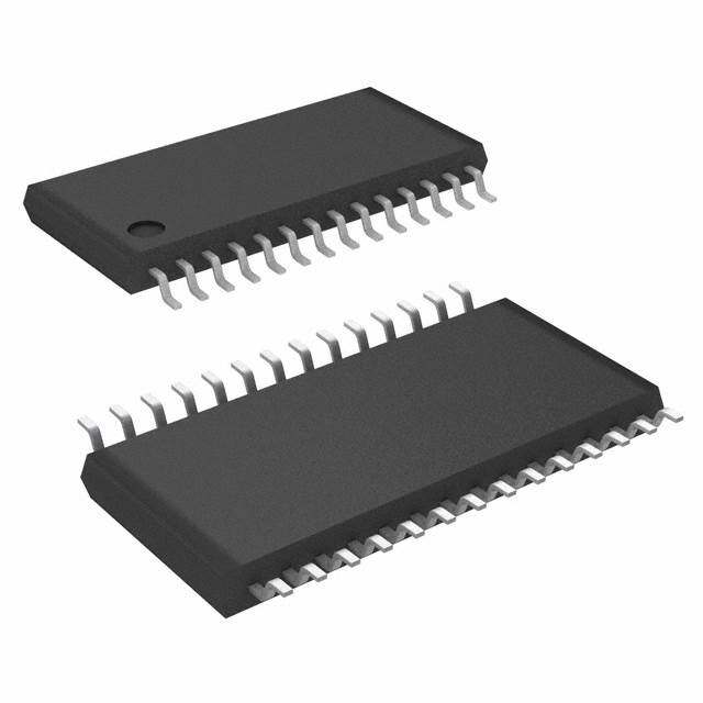
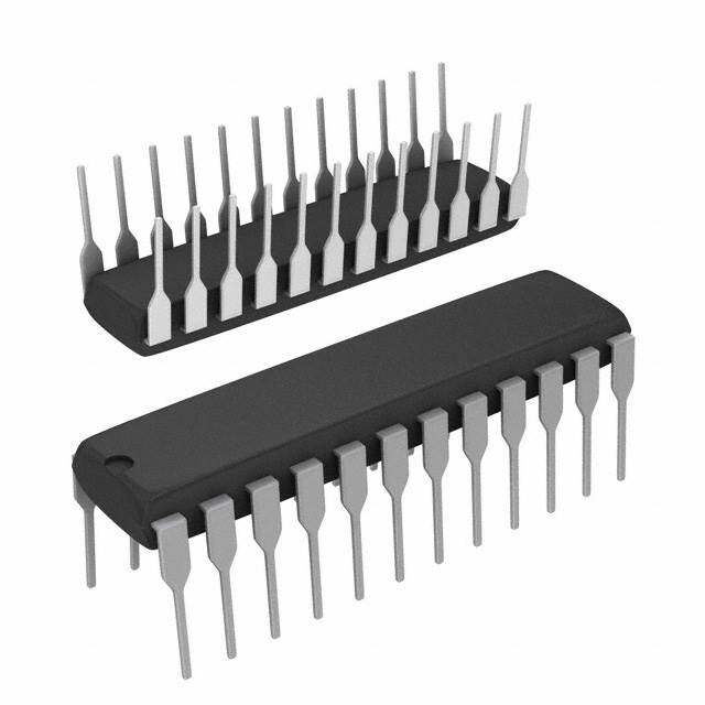
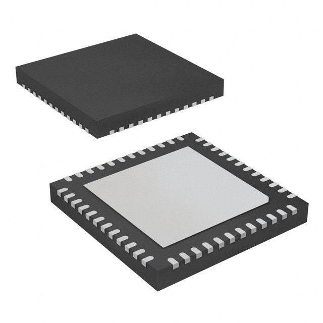
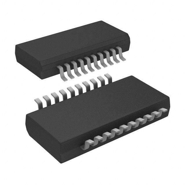
ICGOO在线商城 > 集成电路(IC) > 数据采集 - 模数转换器 > ADS7888SDCKR
- 型号: ADS7888SDCKR
- 制造商: Texas Instruments
- 库位|库存: xxxx|xxxx
- 要求:
| 数量阶梯 | 香港交货 | 国内含税 |
| +xxxx | $xxxx | ¥xxxx |
查看当月历史价格
查看今年历史价格
ADS7888SDCKR产品简介:
ICGOO电子元器件商城为您提供ADS7888SDCKR由Texas Instruments设计生产,在icgoo商城现货销售,并且可以通过原厂、代理商等渠道进行代购。 ADS7888SDCKR价格参考¥11.16-¥22.54。Texas InstrumentsADS7888SDCKR封装/规格:数据采集 - 模数转换器, 8 Bit Analog to Digital Converter 1 Input 1 SAR SC-70-6。您可以下载ADS7888SDCKR参考资料、Datasheet数据手册功能说明书,资料中有ADS7888SDCKR 详细功能的应用电路图电压和使用方法及教程。
| 参数 | 数值 |
| 产品目录 | 集成电路 (IC)半导体 |
| 描述 | IC ADC 8BIT 1.25MSPS SC70-6模数转换器 - ADC 2.35V-5.25V 8 Bit 1.25MSPS Serial |
| 产品分类 | |
| 品牌 | Texas Instruments |
| 产品手册 | http://www.ti.com/litv/slas468 |
| 产品图片 |
|
| rohs | RoHS 合规性豁免含铅 / 不符合限制有害物质指令(RoHS)规范要求 |
| 产品系列 | 数据转换器IC,模数转换器 - ADC,Texas Instruments ADS7888SDCKRmicroPOWER™ |
| 数据手册 | |
| 产品型号 | ADS7888SDCKR |
| 产品培训模块 | http://www.digikey.cn/PTM/IndividualPTM.page?site=cn&lang=zhs&ptm=13240 |
| 产品种类 | 模数转换器 - ADC |
| 位数 | 8 |
| 供应商器件封装 | SC-70-6 |
| 信噪比 | 49.5 dB |
| 其它名称 | 296-32019-6 |
| 分辨率 | 8 bit |
| 制造商产品页 | http://www.ti.com/general/docs/suppproductinfo.tsp?distId=10&orderablePartNumber=ADS7888SDCKR |
| 包装 | Digi-Reel® |
| 商标 | Texas Instruments |
| 安装类型 | 表面贴装 |
| 安装风格 | SMD/SMT |
| 封装 | Reel |
| 封装/外壳 | 6-TSSOP,SC-88,SOT-363 |
| 封装/箱体 | SC-70-6 |
| 工作温度 | -40°C ~ 125°C |
| 工作电源电压 | 2.5 V, 3.3 V, 5 V |
| 工厂包装数量 | 3000 |
| 接口类型 | Serial, SPI |
| 数据接口 | 串行 |
| 最大功率耗散 | 7.5 mW |
| 最大工作温度 | + 125 C |
| 最小工作温度 | - 40 C |
| 标准包装 | 1 |
| 特性 | - |
| 电压参考 | Internal |
| 电压源 | 单电源 |
| 系列 | ADS7888 |
| 结构 | SAR |
| 转换器数 | 1 |
| 转换器数量 | 1 |
| 转换速率 | 1250 kS/s |
| 输入数和类型 | 1 个单端,单极 |
| 输入类型 | Single-Ended |
| 通道数量 | 1 Channel |
| 采样率(每秒) | 1.25M |


- 商务部:美国ITC正式对集成电路等产品启动337调查
- 曝三星4nm工艺存在良率问题 高通将骁龙8 Gen1或转产台积电
- 太阳诱电将投资9.5亿元在常州建新厂生产MLCC 预计2023年完工
- 英特尔发布欧洲新工厂建设计划 深化IDM 2.0 战略
- 台积电先进制程称霸业界 有大客户加持明年业绩稳了
- 达到5530亿美元!SIA预计今年全球半导体销售额将创下新高
- 英特尔拟将自动驾驶子公司Mobileye上市 估值或超500亿美元
- 三星加码芯片和SET,合并消费电子和移动部门,撤换高东真等 CEO
- 三星电子宣布重大人事变动 还合并消费电子和移动部门
- 海关总署:前11个月进口集成电路产品价值2.52万亿元 增长14.8%



PDF Datasheet 数据手册内容提取
Product Sample & Technical Tools & Support & Folder Buy Documents Software Community ADS7887,ADS7888 SLAS468A–JUNE2005–REVISEDAUGUST2016 ADS788x 10-Bit, 8-Bit, 1.25-MSPS, Micro-Power, Miniature SAR Analog-to-Digital Converters 1 Features 3 Description • 1.25-MHzSampleRateSerialDevice The ADS7887 device is a 10-bit, 1.25-MSPS, analog- 1 to-digital converter (ADC), and the ADS7888 device • 10-BitResolution(ADS7887) is a 8-bit, 1.25-MSPS ADC. These devices include a • 8-BitResolution(ADS7888) capacitor-based SAR A/D converter with inherent • ZeroLatency sample and hold. The serial interface in each device is controlled by the CS and SCLK signals for glueless • 25-MHzSerialInterface connections with microprocessors and DSPs. The • SupplyRange:2.35Vto5.25V input signal is sampled with the falling edge of CS, • TypicalPowerDissipationat1.25MSPS: and SCLK is used for conversion and serial data output. – 3.8mWat3-VV DD – 8mwat5-VV The devices operate from a wide supply range from DD 2.35 V to 5.25 V. The low power consumption of the • ±0.35LSBINL,DNL(ADS7887) devices make them suitable for battery-powered • ±0.15LSBINL, ±0.1LSBDNL(ADS7888) applications. The devices also include a power- • 61dBSINAD,–84dBTHD(ADS7887) saving, power-down feature for when the devices are • 49.5dBSINAD, –67.5dBTHD(ADS7888) operatedatlowerconversionspeeds. • UnipolarInputRange:0VtoV The high level of the digital input to the device is not DD limitedtodeviceV .Thismeansthedigitalinputcan • Power-DownCurrent:1 µA DD go as high as 5.25 V when device supply is 2.35 V. • WideInputBandwidth:15MHzat3dB This feature is useful when digital signals are coming • 6-PinSOT23andSC70Packages from other circuit with different supply levels. Also this relaxesrestrictiononpower-upsequencing. 2 Applications The ADS7887 and ADS7888 are available in 6-pin • BaseBandConvertersinRadioCommunication SOT-23 and SC70 packages and are specified for operationfrom–40°Cto125°C. • MotorCurrentandBusVoltageSensorsinDigital Drives DeviceInformation(1) • OpticalNetworking(DWDM,MEMS-Based PARTNUMBER PACKAGE BODYSIZE(NOM) Switching) ADS7887 SOT-23(6) 2.90mm×1.60mm • OpticalSensors ADS7888 SC70(6) 2.00mm×1.25mm • Battery-PoweredSystems (1) For all available packages, see the orderable addendum at • MedicalInstrumentations theendofthedatasheet. • High-SpeedDataAcquisitionSystems • High-SpeedClosed-LoopSystems FunctionalBlockDiagram SAR OUTPUT LATCHES AND SDO 3−STATE +IN CDAC DRIVERS COMPARATOR VDD CONVERSION AND SCLK ADS7887/ADS7888 CONTROL CS LOGIC Copyright © 2016,Texas Instruments Incorporated 1 An IMPORTANT NOTICE at the end of this data sheet addresses availability, warranty, changes, use in safety-critical applications, intellectualpropertymattersandotherimportantdisclaimers.PRODUCTIONDATA.
ADS7887,ADS7888 SLAS468A–JUNE2005–REVISEDAUGUST2016 www.ti.com Table of Contents 1 Features.................................................................. 1 9.3 FeatureDescription.................................................17 2 Applications........................................................... 1 9.4 DeviceFunctionalModes........................................18 3 Description............................................................. 1 10 ApplicationandImplementation........................ 20 4 RevisionHistory..................................................... 2 10.1 ApplicationInformation..........................................20 10.2 TypicalApplication................................................20 5 CompanionProducts............................................. 3 11 PowerSupplyRecommendations..................... 22 6 DeviceComparison............................................... 4 12 Layout................................................................... 23 7 PinConfigurationandFunctions......................... 5 12.1 LayoutGuidelines.................................................23 8 Specifications......................................................... 6 12.2 LayoutExample....................................................23 8.1 AbsoluteMaximumRatings......................................6 13 DeviceandDocumentationSupport................. 24 8.2 ESDRatings..............................................................6 13.1 DocumentationSupport........................................24 8.3 RecommendedOperatingConditions.......................6 13.2 RelatedLinks........................................................24 8.4 ThermalInformation..................................................6 13.3 ReceivingNotificationofDocumentationUpdates24 8.5 ElectricalCharacteristics–ADS7887.......................7 13.4 CommunityResources..........................................24 8.6 ElectricalCharacteristics–ADS7888.......................8 13.5 Trademarks...........................................................24 8.7 TimingRequirements................................................9 13.6 ElectrostaticDischargeCaution............................24 8.8 TypicalCharacteristics............................................10 13.7 Glossary................................................................24 9 DetailedDescription............................................ 16 14 Mechanical,Packaging,andOrderable 9.1 Overview ................................................................16 Information........................................................... 25 9.2 FunctionalBlockDiagram.......................................16 4 Revision History NOTE:Pagenumbersforpreviousrevisionsmaydifferfrompagenumbersinthecurrentversion. ChangesfromOriginal(June2005)toRevisionA Page • AddedESDRatingstable,FeatureDescriptionsection,DeviceFunctionalModes,ApplicationandImplementation section,PowerSupplyRecommendationssection,Layoutsection,DeviceandDocumentationSupportsection,and Mechanical,Packaging,andOrderableInformationsection.................................................................................................. 1 • ChangedThermalInformationtable....................................................................................................................................... 6 2 SubmitDocumentationFeedback Copyright©2005–2016,TexasInstrumentsIncorporated ProductFolderLinks:ADS7887 ADS7888
ADS7887,ADS7888 www.ti.com SLAS468A–JUNE2005–REVISEDAUGUST2016 5 Companion Products PARTNUMBER NAME SN74LVTH245A 3.3-VABTOctalBusTransceiversWith3-StateOutputs LMV761 LowVoltage,PrecisionComparatorwithPush-PullOutput TPS54418 2.95Vto6VInput,4ASynchronousStep-DownSWIFT™Converter LMV339 QuadGeneralPurposeLow-VoltageComparators TPS730 Low-Noise,HighPSRR,RF200-mALow-DropoutLinearRegulators Copyright©2005–2016,TexasInstrumentsIncorporated SubmitDocumentationFeedback 3 ProductFolderLinks:ADS7887 ADS7888
ADS7887,ADS7888 SLAS468A–JUNE2005–REVISEDAUGUST2016 www.ti.com 6 Device Comparison BIT <300KSPS 300KSPS–1.25MSPS 12-Bit ADS7866(1.2V to3.6V ) ADS7886(2.35V to5.25V ) DD DD DD DD 10-Bit ADS7867(1.2V to3.6V ) ADS7887(2.35V to5.25V ) DD DD DD DD 8-Bit ADS7868(1.2V to3.6V ) ADS7888(2.35V to5.25V ) DD DD DD DD 4 SubmitDocumentationFeedback Copyright©2005–2016,TexasInstrumentsIncorporated ProductFolderLinks:ADS7887 ADS7888
ADS7887,ADS7888 www.ti.com SLAS468A–JUNE2005–REVISEDAUGUST2016 7 Pin Configuration and Functions DBVorDCKPackage 6-PinSOT-23orSC70 TopView VDD 1 6 CS GND 2 5 SDO VIN 3 4 SCLK Not to scale PinFunctions PIN I/O DESCRIPTION NO. NAME 1 V — PowersupplyinputalsoactslikeareferencevoltagetoADC. DD 2 GND — Groundforpowersupply,allanaloganddigitalsignalsarereferredwithrespecttothispin. 3 VIN I Analogsignalinput 4 SCLK I Serialclock 5 SDO O Serialdataout 6 CS I Chipselectsignal,activelow Copyright©2005–2016,TexasInstrumentsIncorporated SubmitDocumentationFeedback 5 ProductFolderLinks:ADS7887 ADS7888
ADS7887,ADS7888 SLAS468A–JUNE2005–REVISEDAUGUST2016 www.ti.com 8 Specifications 8.1 Absolute Maximum Ratings overoperatingfree-airtemperaturerange(unlessotherwisenoted)(1) MIN MAX UNIT +INtoAGND –0.3 V +0.3 V DD +V toAGND –0.3 7 V DD DigitalinputvoltagetoGND –0.3 7 V DigitaloutputtoGND –0.3 V +0.3 V DD Powerdissipation,bothpackages (T –T )/R J(MAX) A θJA Vaporphase(60s) 215 Leadtemperature,soldering °C Infrared(15s) 220 Junctiontemperature,T 150 °C J(MAX) Storagetemperature,T –65 150 °C stg (1) StressesbeyondthoselistedunderAbsoluteMaximumRatingsmaycausepermanentdamagetothedevice.Thesearestressratings only,whichdonotimplyfunctionaloperationofthedeviceattheseoranyotherconditionsbeyondthoseindicatedunderRecommended OperatingConditions.Exposuretoabsolute-maximum-ratedconditionsforextendedperiodsmayaffectdevicereliability. 8.2 ESD Ratings VALUE UNIT Human-bodymodel(HBM),perANSI/ESDA/JEDECJS-001(1) ±2000 V Electrostaticdischarge V (ESD) Charged-devicemodel(CDM),perJEDECspecificationJESD22-C101(2) ±500 (1) JEDECdocumentJEP155statesthat500-VHBMallowssafemanufacturingwithastandardESDcontrolprocess. (2) JEDECdocumentJEP157statesthat250-VCDMallowssafemanufacturingwithastandardESDcontrolprocess. 8.3 Recommended Operating Conditions overoperatingfree-airtemperaturerange(unlessotherwisenoted) MIN MAX UNIT T Operatingtemperature –40 125 °C A 8.4 Thermal Information ADS7887,ADS7888 THERMALMETRIC(1) DBV(SOT-23) DCK(SC70) UNIT 6PINS 6PINS R Junction-to-ambientthermalresistance 114.9 150.7 °C/W θJA R Junction-to-case(top)thermalresistance 56.6 62.3 °C/W θJC(top) R Junction-to-boardthermalresistance 36.5 43 °C/W θJB ψ Junction-to-topcharacterizationparameter 5.8 1.8 °C/W JT ψ Junction-to-boardcharacterizationparameter 36.2 42.4 °C/W JB R Junction-to-case(bottom)thermalresistance — — °C/W θJC(bot) (1) Formoreinformationabouttraditionalandnewthermalmetrics,seetheSemiconductorandICPackageThermalMetricsapplication report. 6 SubmitDocumentationFeedback Copyright©2005–2016,TexasInstrumentsIncorporated ProductFolderLinks:ADS7887 ADS7888
ADS7887,ADS7888 www.ti.com SLAS468A–JUNE2005–REVISEDAUGUST2016 8.5 Electrical Characteristics – ADS7887 +V =2.35Vto5.25V,T =–40°Cto125°C,andf =1.25MHz(unlessotherwisenoted) DD A sample PARAMETER TESTCONDITIONS MIN TYP MAX UNIT ANALOGINPUT Full-scaleinputvoltagespan(1) 0 V V DD Absoluteinputvoltagerange +IN –0.2 V +0.2 V DD C Inputcapacitance(2) 21 pF i I Inputleakagecurrent T =125°C 40 nA Ilkg A SYSTEMPERFORMANCE Resolution 10 Bits Nomissingcodes 10 Bits INL Integralnonlinearity –0.75 ±0.35 0.75 LSB(3) DNL Differentialnonlinearity –0.5 ±0.35 0.5 LSB E Offseterror(4)(5)(6) –1.5 ±0.5 1.5 LSB O E Gainerror(5) –1 ±0.5 1 LSB G SAMPLINGDYNAMICS Conversiontime 25-MHzSCLK 530 560 ns Acquisitiontime 260 ns Maximumthroughputrate 25-MHzSCLK 1.25 MHz Aperturedelay 5 ns StepResponse 160 ns Overvoltagerecovery 160 ns DYNAMICCHARACTERISTICS THD Totalharmonicdistortion(7) 100kHz –84 –72 dB SINAD Signal-to-noiseanddistortion 100kHz 60.5 61 dB SFDR Spuriousfreedynamicrange 100kHz 73 81 dB Fullpowerbandwidth At–3dB 15 MHz DIGITALINPUT/OUTPUT V High-levelinputvoltage VDD=2.35Vto5.25V V –0.4 5.25 V IH DD V =5V 0.8 DD V Low-levelinputvoltage V IL V =3V 0.4 DD V High-leveloutputvoltage AtI =200µA V –0.2 OH source DD V V Low-leveloutputvoltage AtI =200µA 0.4 OL sink POWERSUPPLYREQUIREMENTS +V Supplyvoltage 2.35 3.3 5.25 V DD AtV =2.35Vto5.25V, DD 2 Supplycurrent(normalmode) 1.25-MHzthroughput mA AtV =2.35Vto5.25V,staticstate 1.5 DD SCLKoff 1 Power-downstatesupplycurrent µA SCLKon(25MHz) 200 Powerdissipation VDD=5V 8 10 mW at1.25-MHzthroughput V =3V 3.8 6 DD V =5V 5.5 7.5 DD Powerdissipationinstaticstate mW V =3V 3 4.5 DD Power-downtime 0.1 µs (1) Idealinputspan;doesnotincludegainoroffseterror. (2) ReferFigure31fordetailsonsamplingcircuit (3) LSBmeansleastsignificantbit (4) Measuredrelativetoanidealfull-scaleinput (5) Offseterrorandgainerrorensuredbycharacterization. (6) Firsttransitionof000Hto001Hat0.5×(V /210) ref (7) Calculatedonthefirstnineharmonicsoftheinputfrequency Copyright©2005–2016,TexasInstrumentsIncorporated SubmitDocumentationFeedback 7 ProductFolderLinks:ADS7887 ADS7888
ADS7887,ADS7888 SLAS468A–JUNE2005–REVISEDAUGUST2016 www.ti.com Electrical Characteristics – ADS7887 (continued) +V =2.35Vto5.25V,T =–40°Cto125°C,andf =1.25MHz(unlessotherwisenoted) DD A sample PARAMETER TESTCONDITIONS MIN TYP MAX UNIT Power-uptime 0.8 µs Invalidconversionsafterpowerup 1 8.6 Electrical Characteristics – ADS7888 +V =2.35Vto5.25V,T =–40°Cto125°C,andf =1.25MHz(unlessotherwisenoted) DD A sample PARAMETER TESTCONDITIONS MIN TYP MAX UNIT ANALOGINPUT Full-scaleinputvoltagespan(1) 0 V V DD Absoluteinputvoltagerange +IN –0.2 V +0.2 V DD C Inputcapacitance(2) 21 pF i I Inputleakagecurrent T =125°C 40 nA Ilkg A SYSTEMPERFORMANCE Resolution 8 Bits Nomissingcodes 8 Bits INL Integralnonlinearity –0.3 ±0.15 0.3 LSB(3) DNL Differentialnonlinearity –0.3 ±0.1 0.3 LSB E Offseterror(4) (5) (6) –0.5 ±0.15 0.5 LSB O E Gainerror(5) –0.5 ±0.15 0.5 LSB G SAMPLINGDYNAMICS Conversiontime 25-MHzSCLK 450 480 ns Acquisitiontime 1.5MSPSmode,seeFigure34 206 ns Maximumthroughputrate 25-MHzSCLK 1.25 MHz Aperturedelay 5 ns StepResponse 160 ns Overvoltagerecovery 160 ns DYNAMICCHARACTERISTICS THD Totalharmonicdistortion(7) 100kHz –67.5 –65 dB SINAD Signal-to-noiseanddistortion 100kHz 49 49.5 dB SFDR Spuriousfreedynamicrange 100kHz 65 77 dB Fullpowerbandwidth At–3dB 15 MHz DIGITALINPUT/OUTPUT V High-levelinputvoltage V =2.35Vto5.25V V –0.4 5.25 V IH DD DD V =5V 0.8 DD V Low-levelinputvoltage V IL V =3V 0.4 DD V High-leveloutputvoltage AtI =200µA V –0.2 OH source DD V V Low-leveloutputvoltage AtI =200µA 0.4 OL sink POWERSUPPLYREQUIREMENTS +V Supplyvoltage 2.35 3.3 5.25 V DD AtV =2.35Vto5.25V,1.25-MHz DD 2 Supplycurrent(normalmode) throughput mA AtV =2.35Vto5.25V,staticstate 1.5 DD (1) Idealinputspan;doesnotincludegainoroffseterror. (2) ReferFigure31fordetailsonsamplingcircuit (3) LSBmeansleastsignificantbit (4) Measuredrelativetoanidealfull-scaleinput (5) Offseterrorandgainerrorensuredbycharacterization. (6) Firsttransitionof000Hto001Hat(V /28) ref (7) Calculatedonthefirstnineharmonicsoftheinputfrequency 8 SubmitDocumentationFeedback Copyright©2005–2016,TexasInstrumentsIncorporated ProductFolderLinks:ADS7887 ADS7888
ADS7887,ADS7888 www.ti.com SLAS468A–JUNE2005–REVISEDAUGUST2016 Electrical Characteristics – ADS7888 (continued) +V =2.35Vto5.25V,T =–40°Cto125°C,andf =1.25MHz(unlessotherwisenoted) DD A sample PARAMETER TESTCONDITIONS MIN TYP MAX UNIT SCLKoff 1 Power-downstatesupplycurrent µA SCLKon(25MHz) 200 Powerdissipationat1.25MHz VDD=5V 8 10 mW throughput V =3V 3.8 6 DD V =5V 5.5 7.5 DD Powerdissipationinstaticstate mW V =3V 3 4.5 DD Power-downtime 0.1 µs Power-uptime 0.8 µs Invalidconversionsafterpowerup 1 8.7 Timing Requirements AllspecificationstypicalatT =–40°Cto125°CandV =2.35Vto5.25V(unlessotherwisenoted;seeFigure32) A DD PARAMETER TESTCONDITIONS(1) MIN TYP MAX UNIT V =3V 14×t DD SCLK ADS7887 V =5V 14×t DD SCLK t Conversiontime ns conv V =3V 12×t DD SCLK ADS7888 V =5V 12×t DD SCLK Minimumtimerequiredfrombus3-state VDD=3V 40 t Quiettime ns q tostartofnextconversion V =5V 40 DD V =3V 15 25 DD t Delaytime CSlowtofirstdata(0)out ns d1 V =5V 13 25 DD V =3V 10 DD t Setuptime CSlowtoSCLKlow ns su1 V =5V 10 DD V =3V 15 25 DD t Delaytime SCLKfallingtoSDO ns d2 V =5V 13 25 DD SCLKfallingtodatavalid(with50-pF VDD<3V 7 t Holdtime ns h1 load) V >5V 5.5 DD V =3V 10 25 DD t Delaytime 16thSCLKfallingedgetoSDO3-state ns d3 V =5V 8 20 DD V =3V 25 40 DD t Pulseduration CS ns w1 V =5V 25 40 DD V =3V 17 30 DD t Delaytime CShightoSDO3-state,seeFigure34 ns d4 V =5V 15 25 DD V =3V 0.4×t DD SCLK t Pulseduration SCLKhigh ns wH V =5V 0.4×t DD SCLK V =3V 0.4×t DD SCLK t Pulseduration SCLKlow ns wL V =5V 0.4×t DD SCLK V =3V 25 DD Frequency SCLK MHz V =5V 25 DD SecondfallingedgeofclockandCSto V =3V –2 5 DD enterinpowerdown(useminspecnotto t Delaytime ns d5 accidentlyenterinpowerdown,see V =5V –2 5 DD Figure35) CSand10thfallingedgeofclocktoenter V =3V 2 –5 DD inpowerdown(usemaxspecnotto t Delaytime ns d6 accidentlyenterinpowerdown,see V =5V 2 –5 DD Figure35) (1) 3-VSpecificationsapplyfrom2.35Vto3.6V,and5-Vspecificationsapplyfrom4.75Vto5.25V. Copyright©2005–2016,TexasInstrumentsIncorporated SubmitDocumentationFeedback 9 ProductFolderLinks:ADS7887 ADS7888
ADS7887,ADS7888 SLAS468A–JUNE2005–REVISEDAUGUST2016 www.ti.com 8.8 Typical Characteristics 8.8.1 ADS7887andADS7888 1.8 1.80 TA= 25°C 1.7 ffsSC=L 1K.2=5 2 M5 SMPHSz, 1.60 5 V VDD mA 1.6 25°C mA 1.40 − − Current 1.5 125°C Current 1.210 2.35 V VDD ply 1.4 ply p p 0.80 u u −SD 1.3 −40°C −SD 0.60 D D I 1.2 I 0.40 1.1 0.20 1 0 2.35 3.075 3.8 4.525 5.25 0 5 10 15 20 25 VDD−Supply Voltage−V fSCLK−SCLK Frequency−MHz Figure1.SupplyCurrentvsSupplyVoltage Figure2.SupplyCurrentvsSCLKFrequency 1.4 30 VDD= 5 V, fSCLK= 25 MHz, 1.2 TA= 25°C, 20 Power Down SCLK = Free Running A m − 1 A 10 @ 5 V Input ent −n ply Curr 0.8 Current 0 Sup 0.6 age −10 −D eak D 0.4 L −20 @ 0 V Input I 0.2 −30 0 −40 0 50 100 150 200 250 300 350 400 450 −40 −20 0 20 40 60 80 100 120 fs−Sample Rate−KSPS TA−Free-Air Temperature−°C Figure3.SupplyCurrentvsSampleRate Figure4.AnalogInputLeakageCurrent vsFree-AirTemperature 10 SubmitDocumentationFeedback Copyright©2005–2016,TexasInstrumentsIncorporated ProductFolderLinks:ADS7887 ADS7888
ADS7887,ADS7888 www.ti.com SLAS468A–JUNE2005–REVISEDAUGUST2016 8.8.2 ADS7887Only 62 −dB 61.9 fTVsAD=D= 1 =2. 2555° CV M,SPS, −dB 61.9 ffTsiA=== 11 20.2505° kC MHzS,PS, on 61.7 on 61.8 orti orti Dist 61.5 Dist 61.7 nd nd 61.6 e a 61.3 e a ois ois 61.5 N N o- 61.1 o- 61.4 al-t al-t Sign 60.9 Sign 61.3 − − 61.2 D D A 60.7 A SIN SIN 61.1 60.5 61 1 10 100 1000 2.35 3.075 3.8 4.525 5.25 fi−Input Frequency−kHz VDD−Supply Voltage−V Figure5.Signal-to-NoiseandDistortion Figure6.Signal-to-NoiseandDistortion vsInputFrequency vsSupplyVoltage −80 −80 −dB −−8821 fTVsAD=D= 1 =2. 2555° CV MSPS, −dB −−8821 ffTsiA=== 11 20.2505° C kMHSzP,S, n n ortio −83 ortio −83 Dist −84 Dist −84 c c oni −85 oni −85 m m ar −86 ar −86 H H Total −87 otal T −87 D− −88 D− −88 H H T T −89 −89 −90 −90 1 10 100 2.35 3.075 3.8 4.525 5.25 fi−Input Frequency−kHz VDD−Supply Voltage−V Figure7.TotalHarmonicDistortion Figure8.TotalHarmonicDistortion vsInputFrequency vsSupplyVoltage 85 85 dB 84.5 fTsA== 1 2.255°C M,SPS, dB 84.5 ffsi== 110.205 kMHSzP,S, mic Range− 838.45 VDD= 5 V mic Range− 838.45 TA= 25°C Dyna 83 Dyna 83 Spurious Free 88128..255 Spurious Free 88128..255 − 81 − 81 SFDR 80.5 SFDR 80.5 80 80 1 10 100 2.35 3.075 3.8 4.525 5.25 fi−Input Frequency−kHz VDD−Supply Voltage−V Figure9.SpuriousFreeDynamicRange Figure10.SpuriousFreeDynamicRange vsInputFrequency vsSupplyVoltage Copyright©2005–2016,TexasInstrumentsIncorporated SubmitDocumentationFeedback 11 ProductFolderLinks:ADS7887 ADS7888
ADS7887,ADS7888 SLAS468A–JUNE2005–REVISEDAUGUST2016 www.ti.com ADS7887 Only (continued) 1 1 0.8 fTsA== 1 2.255°C MSPS, 0.8 fVsD=D 1=. 255 V MSPS, 0.6 0.6 Offset Error−LSBs −000...2402 Offset Error−LSBs −000...2402 E−O −0.4 E−O −0.4 −0.6 −0.6 −0.8 −0.8 −1 −1 2.35 3.075 3.8 4.525 5.25 −40 −20 0 20 40 60 80 100 120 VDD−Supply Voltage−V TA−Free-Air Temperature−°C Figure11.OffsetErrorvsSupplyVoltage Figure12.OffsetErrorvsFree-AirTemperature 1 1 0.8 fTsA== 1 2.255°C MSPS, 0.8 fVsD=D 1=. 255 V MSPS, 0.6 0.6 E−Gain Error−LSBsG −−0000....24042 E−Gain Error−LSBsG −−0000....24042 −0.6 −0.6 −0.8 −0.8 −1 −1 2.35 3.075 3.8 4.525 5.25 −40 −20 0 20 40 60 80 100 120 VDD−Supply Voltage−V TA−Free-Air Temperature−°C Figure13.GainErrorvsSupplyVoltage Figure14.GainErrorvsFree-AirTemperature 0.5 0.5 00..34 VfTsAD=D= 1 =2. 2525°.C3 M5 SVP,S, 00..34 VfTsAD=D= 1 =2. 2525°.C3 M5 SVP,S, D−NLLSBs −−0000....12021 INL−LSBs −−0000....12021 −0.3 −0.3 −0.4 −0.4 −0.5 −0.5 0 256 512 768 1024 0 256 512 768 1024 Output Code Output Code Figure15.DNL Figure16.INL 12 SubmitDocumentationFeedback Copyright©2005–2016,TexasInstrumentsIncorporated ProductFolderLinks:ADS7887 ADS7888
ADS7887,ADS7888 www.ti.com SLAS468A–JUNE2005–REVISEDAUGUST2016 ADS7887 Only (continued) 0 −20 VDD= 2.35 V, fs= 1.25 MSPS, dB −40 TA= 25°C − fi= 100 kHz, de −60 8192 Points u plit −80 m A −100 −120 −140 0 125000 250000 375000 500000 625000 fi−Input Frequency−kHz Figure17.FFT 8.8.3 ADS7888Only 50 50 Signal-to-Noise and Distortion−dB 44444449999999.......3456789 fTVsAD=D= 1 =2. 2555° CV M,SPS, Signal-to-Noise and Distortion−dB 44444449999999.......3456789 ffTsiA=== 11 20.2505° C kMHSzP,S, SINAD− 4499..12 SINAD− 4499..12 49 49 1 10 100 1000 2.35 3.075 3.8 4.525 5.25 fi−Input Frequency−kHz VDD−Supply Voltage−V Figure18.Signal-to-NoiseandDistortion Figure19.Signal-to-NoiseandDistortion vsInputFrequency vsSupplyVoltage −65 −65 VDD= 5 V, fi= 100 kHz, monic Distortion−dB −−−666−−76566...55576 fTsA== 1 2.255°C MSPS, monic Distortion−dB −−−666−−76566...55576 fTsA== 1 2.255°C MSPS, otTal Har −6−86.58 Total Har −6−86.58 − − THD −69 THD −69 −69.5 −69.5 −70 −701 10 100 2.35 3.075 3.8 4.525 5.25 fi−Input Frequency−kHz VDD−Supply Voltage−V Figure20.TotalHarmonicDistortion Figure21.TotalHarmonicDistortion vsInputFrequency vsSupplyVoltage Copyright©2005–2016,TexasInstrumentsIncorporated SubmitDocumentationFeedback 13 ProductFolderLinks:ADS7887 ADS7888
ADS7887,ADS7888 SLAS468A–JUNE2005–REVISEDAUGUST2016 www.ti.com ADS7888 Only (continued) 80 85 mic Range−dB 77897..955 VfTsAD=D= 1 =2. 2555° CV M,SPS, mic Range−dB 888234 ffTisA=== 11 02.2055 °kC MHzS,PS, Spurious Free Dyna 776777..7855 Spurious Free Dyna 77888901 SFDR− 757.65 SFDR− 7767 75 75 1 10 100 2.35 3.075 3.8 4.525 5.25 fi−Input Frequency−kHz VDD−Supply Voltage−V Figure22.SpuriousFreeDynamicRange Figure23.SpuriousFreeDynamicRange vsInputFrequency vsSupplyVoltage 0.3 0.3 fTsA== 1 2.255°C MSPS, fVsD=D 1=. 255 V MSPS, 0.2 0.2 s s B B S S L 0.1 L 0.1 − − or or et Err 0 et Err 0 s s Off Off − −0.1 − −0.1 O O E E −0.2 −0.2 −0.3 −0.3 2.35 3.075 3.8 4.525 5.25 −40 −7 26 59 92 125 VDD−Supply Voltage−V TA−Free-Air Temperature−°C Figure24.OffsetErrorvsSupplyVoltage Figure25.OffsetErrorvsFree-AirTemperature 0.3 0.3 0.2 fTsA== 1 2.255°C MSPS, 0.2 fTsA== 1 2.255°C MSPS, Gain Error−LSBs 0.10 Gain Error−LSBs 0.10 E−G −0.1 E−G −0.1 −0.2 −0.2 −0.3 −0.3 2.35 3.075 3.8 4.525 5.25 −40 −7 26 59 92 125 VDD−Supply Voltage−V TA−Free-Air Temperature−°C Figure26.GainErrorvsSupplyVoltage Figure27.GainErrorvsFree-AirTemperature 14 SubmitDocumentationFeedback Copyright©2005–2016,TexasInstrumentsIncorporated ProductFolderLinks:ADS7887 ADS7888
ADS7887,ADS7888 www.ti.com SLAS468A–JUNE2005–REVISEDAUGUST2016 ADS7888 Only (continued) 0.5 0.5 00..34 VfTsAD=D= 1 =2. 2525°.C3 M5 SVP,S, 00..34 VfTsAD=D= 1 =2. 2525°.C3 M5 SVP,S, DNL−LSBs −−0000....12021 INL−LSBs −−0000....12021 −0.3 −0.3 −0.4 −0.4 −0.5 −0.5 0 64 128 192 256 0 64 128 192 256 Output Code Output Code Figure28.DNL Figure29.INL 0 −20 TA= 25°C fi= 100 kHz, B 8192 Points d − −40 e d u −60 plit m A −80 −100 −120 0 125000 250000 375000 500000 625000 fi−Input Frequency−kHz Figure30.FFT Copyright©2005–2016,TexasInstrumentsIncorporated SubmitDocumentationFeedback 15 ProductFolderLinks:ADS7887 ADS7888
ADS7887,ADS7888 SLAS468A–JUNE2005–REVISEDAUGUST2016 www.ti.com 9 Detailed Description 9.1 Overview The ADS788x devices are ADC converters. The serial interface in each device is controlled by the CS and SCLK signals for easy interface with microprocessors and DSPs. The input signal is sampled with the falling edge of CS,andSCLKisusedforconversionandserialdataoutput.Theybothoperateinawidesupplyrangefrom2.35 Vto5.25Vandlowpowerconsumptionmakesthemsuitableforbattery-poweredapplications. 9.1.1 DrivingtheVINandV PinsoftheADS7887andADS7888 DD The VIN input to the ADS7887 and ADS7888 must be driven with a low impedance source. In most cases additional buffers are not required. In cases where the source impedance exceeds 200 Ω, using a buffer would help achieve the rated performance of the converter. The THS4031 is a good choice for the driver amplifier buffer. The reference voltage for the ADS7887 and ADS7888 A/D converters are derived from the supply voltage internally. The devices offer limited low-pass filtering functionality on-chip. The supply to these converters must be driven with a low impedance source and must be decoupled to the ground. A 1-µF storage capacitor and a 10-nF decoupling capacitor must be placed close to the device. Wide, low impedance traces must be used to connect the capacitor to the pins of the device. The ADS7887 and ADS7888 draw very little current from the supplylines.Thesupplylinecanbedrivenbyeither: • Directlyfromthesystemsupply. • A reference output from a low drift and low dropout reference voltage generator like REF3030 or REF3130. The ADS7887 and ADS7888 can operate off a wide range of supply voltages. The actual choice of the referencevoltagegeneratorwoulddependuponthesystem.Figure41showsonepossibleapplicationcircuit. • A low-pass filtered version of the system supply followed by a buffer like the zero-drift OPA735 can also be used in cases where the system power supply is noisy. Take care to ensure that the voltage at the V input DD does not exceed 7 V (especially during power up) to avoid damage to the converter. This can be done easily usingsingle-supplyCMOSamplifiersliketheOPA735.Figure42 showsonepossibleapplicationcircuit. VDD 60W 20W IN 16 pF 5 pF 60W GND Figure31. TypicalEquivalentSamplingCircuit 9.2 Functional Block Diagram SAR OUTPUT LATCHES AND SDO 3−STATE +IN CDAC DRIVERS COMPARATOR VDD CONVERSION SCLK AND ADS7887/ADS7888 CONTROL CS LOGIC Copyright © 2016,Texas Instruments Incorporated 16 SubmitDocumentationFeedback Copyright©2005–2016,TexasInstrumentsIncorporated ProductFolderLinks:ADS7887 ADS7888
ADS7887,ADS7888 www.ti.com SLAS468A–JUNE2005–REVISEDAUGUST2016 9.3 Feature Description 9.3.1 ADS7887Operation The cycle begins with the falling edge of CS. This point is indicated as a in Figure 32. With the falling edge of CS, the input signal is sampled and the conversion process is initiated. The device outputs data while the conversion is in progress. The data word contains 4 leading zeros, followed by 10-bit data in MSB first format andpaddedby2laggingzeros. The falling edge of CS clocks out the first zero, and a zero is clocked out on every falling edge of the clock until thethirdedge.DataisinMSBfirstformatwiththeMSBbeingclockedoutonthe4thfallingedge.Dataispadded with two lagging zeros as shown in Figure 32. On the 16th falling edge of SCLK, SDO goes to the 3-state condition. The conversion ends on the 14th falling edge of SCLK. The device enters the acquisition phase on the firstrisingedgeofSCLKafterthe13thfallingedge.Thispointisindicatedby binFigure32. CS can be asserted (pulled high) after 16 clocks have elapsed. It is necessary not to start the next conversion by pulling CS low until the end of the quiet time (t ) after SDO goes to 3-state. To continue normal operation, it is q necessary that CS is not pulled high until point b. Without this, the device does not enter the acquisition phase and no valid data is available in the next cycle (refer to Power-Down Mode for more details). CS going high any timeaftertheconversionstartabortstheongoingconversionandSDOgoesto3-state. ThehighlevelofthedigitalinputtothedeviceisnotlimitedtodeviceV .Thismeansthedigitalinputcangoas DD high as 5.25 V when the device supply is 2.35 V. This feature is useful when digital signals are coming from another circuit with different supply levels. Also, this relaxes the restriction on power-up sequencing. However, thedigitaloutputlevels(V andV )aregovernedbyV aslistedinSpecifications. OH OL DD a tconv tw1 b CS tsu1 SCLK 1 2 4 5 6 13 14 15 16 td1 td2 th1 td3 SDO 0 0 0 D9 D8 D1 D0 0 0 tq 1/throughput Figure32. ADS7887InterfaceTimingDiagram 9.3.2 ADS7888Operation The cycle begins with the falling edge of CS . This point is indicated as a in Figure 33. With the falling edge of CS, the input signal is sampled and the conversion process is initiated. The device outputs data while the conversion is in progress. The data word contains 4 leading zeros, followed by 8-bit data in MSB first format and paddedby4laggingzeros. The falling edge of CS clocks out the first zero, and a zero is clocked out on every falling edge of the clock until thethirdedge.DataisinMSBfirstformatwiththeMSBbeingclockedoutonthe4thfallingedge.Dataispadded with four lagging zeros as shown in Figure 33. On the 16th falling edge of SCLK, SDO goes to the 3-state condition. The conversion ends on the 12th falling edge of SCLK. The device enters the acquisition phase on the firstrisingedgeofSCLKafterthe11thfallingedge.Thispointisindicatedby binFigure33. CS can be asserted (pulled high) after 16 clocks have elapsed. It is necessary not to start the next conversion by pulling CS low until the end of the quiet time (t ) after SDO goes to 3-state. To continue normal operation, it is q necessary that CS is not pulled high until point b. Without this, the device does not enter the acquisition phase and no valid data is available in the next cycle (refer to Power-Down Mode for more details). CS going high any timeaftertheconversionstartabortstheongoingconversionandSDOgoesto3-state. ThehighlevelofthedigitalinputtothedeviceisnotlimitedtodeviceV .Thismeansthedigitalinputcangoas DD high as 5.25 V when the device supply is 2.35 V. This feature is useful when digital signals are coming from another circuit with different supply levels. Also, this relaxes the restriction on power-up sequencing. However, thedigitaloutputlevels(V andV )aregovernedbyV aslistedinSpecifications. OH OL DD Copyright©2005–2016,TexasInstrumentsIncorporated SubmitDocumentationFeedback 17 ProductFolderLinks:ADS7887 ADS7888
ADS7887,ADS7888 SLAS468A–JUNE2005–REVISEDAUGUST2016 www.ti.com Feature Description (continued) a tconv tw1 b CS tsu1 SCLK 1 2 4 5 6 11 12 15 16 td1 td2 th1 td3 SDO 0 0 0 D7 D6 D1 D0 0 0 0 tq 1/throughput Figure33. ADS7888InterfaceTimingDiagram As shown in Figure 34, the ADS7888 can achieve 1.5-MSPS throughput. CS can be pulled high after the 12th falling edge (with a 25-MHz SCLK). SDO goes to 3-state after the LSB (as CS is high). CS can be pulled low at theendofthequiettime(t )afterSDOgoesto3-state. q a tconv tw1 b CS tsu1 td4 SCLK 1 2 4 5 6 11 12 td1 td2 th1 th1 SDO 0 0 0 D7 D6 D1 D0 tq 1/throughput Figure34. ADS7888InterfaceTimingDiagram,DataTransferWith12-ClockFrame 9.4 Device Functional Modes 9.4.1 Power-DownMode The device enters power-down mode if CS goes high anytime after the 2nd SCLK falling edge to before the 10th SCLK falling edge. Ongoing conversion stops and SDO goes to 3-state under this power-down condition as showninFigure35. td5 td6 CS 1 2 3 4 5 9 10 16 SCLK SDO Figure35. EnteringPower-DownMode Adummycyclewith CSlowformorethan10SCLKfallingedgesbringsthedeviceoutofpower-downmode.For the device to come to the fully powered-up condition it takes 0.8 µs. CS can be pulled high any time after the 10th falling edge as shown in Figure 36. It is not necessary to continue until the 16th clock if the next conversion starts0.8µsafter CSgoinglowofthedummycycleandthequiettime(t )conditionismet. q 18 SubmitDocumentationFeedback Copyright©2005–2016,TexasInstrumentsIncorporated ProductFolderLinks:ADS7887 ADS7888
ADS7887,ADS7888 www.ti.com SLAS468A–JUNE2005–REVISEDAUGUST2016 Device Functional Modes (continued) Device Starts Device Fully Powering Up Powered-Up CS SCLK 1 2 3 4 5 6 7 8 9 10 11 12 13 14 15 16 1 2 3 4 5 6 7 8 9 10 11 12 13 14 15 16 SDO Invalid Data Valid Data Figure36. ExitingPower-DownMode Copyright©2005–2016,TexasInstrumentsIncorporated SubmitDocumentationFeedback 19 ProductFolderLinks:ADS7887 ADS7888
ADS7887,ADS7888 SLAS468A–JUNE2005–REVISEDAUGUST2016 www.ti.com 10 Application and Implementation NOTE Information in the following applications sections is not part of the TI component specification, and TI does not warrant its accuracy or completeness. TI’s customers are responsible for determining suitability of components for their purposes. Customers should validateandtesttheirdesignimplementationtoconfirmsystemfunctionality. 10.1 Application Information The primary circuits required to maximize the performance of a high-precision, the successive approximation register (SAR) and analog-to-digital converter (ADC), are the input driver and the reference driver circuits. This section details some general principles for designing the input driver circuit, references the driver circuit, and providessomeapplicationcircuitsdesignedfortheADS7887andADS7888. 10.2 Typical Application AVDD AVDD OPA365 – 33 (cid:13) VDD VIN + + Device VSOURCE – 680 pF GND GND Device: 10-Bit / 8 bit , 1.25 MSPS, Input Driver Single-Ended Input Copyright © 2016, Texas Instruments Incorporated Figure37. TypicalDataAcquisition(DAQ)Circuit:Single-SupplyDAQ 10.2.1 DesignRequirements The goal of this application is to design a single-supply digital acquisition (DAQ) circuit based on the ADS7887 with SNR greater than 61 dB and THD less than –84 dB for input frequencies of 2 kHz to 100 kHz at a throughputof1.25MSPS. 10.2.2 DetailedDesignProcedure ToachieveaSINADof61dB,theoperationalamplifiermusthavehighbandwidthtosettletheinputsignalwithin the acquisition time of the ADC. The operational amplifier must have low noise to keep the total system noise below 20% of the input-referred noise of the ADC. For the application circuit shown in Figure 37, OPA365 is selectedforitshighbandwidth(50MHz)andlownoise(4.5nV√Hz). The reference voltage for the ADS7887 and ADS7888 A/D converters are derived from the supply voltage internally.Thesupplytotheseconvertersmustbedrivenwithalowimpedancesourceandmustbedecoupledto the ground. To drive supply pin of ADS7887 ultra low noise fast transient response low dropout voltage regulator TPS73201 is selected. Alternatively one can drive supply pin with low impedance voltage reference similar to REF3030. For a step-by-step design procedure for low power, small form factor digital acquisition (DAQ) circuit based on similar SAR ADCs refer to TI Precision Design, Three 12-Bit Data Acquisition Reference Designs Optimized for LowPowerandUltra-SmallFormFactor. 20 SubmitDocumentationFeedback Copyright©2005–2016,TexasInstrumentsIncorporated ProductFolderLinks:ADS7887 ADS7888
ADS7887,ADS7888 www.ti.com SLAS468A–JUNE2005–REVISEDAUGUST2016 Typical Application (continued) 10.2.3 ApplicationCurves SNR:61.9dB THD:–86.8dB SINAD:61.3dB SNR:61.8dB THD:–85.1dB SINAD:61.5dB Figure38.TestResultsfortheADS7887andOPA365fora Figure39.TestResultsfortheADS7887andOPA365fora 2-kHzInput 100-kHzInput Copyright©2005–2016,TexasInstrumentsIncorporated SubmitDocumentationFeedback 21 ProductFolderLinks:ADS7887 ADS7888
ADS7887,ADS7888 SLAS468A–JUNE2005–REVISEDAUGUST2016 www.ti.com 11 Power Supply Recommendations The reference voltage for the ADS7887 and ADS7888 A/D converters are derived from the supply voltage internally.Thesupplytotheseconvertersmustbedrivenwithalowimpedancesourceandmustbedecoupledto the ground Decouple the V with 1-µF ceramic decoupling capacitors, as shown in Figure 40. Always set the DD V supplytobegreaterthanorequaltothemaximuminputsignaltoavoidsaturationofcodes. DD VDD VDD CS VIN SDO 1 µF 10 nF GND SCLK Figure40. SupplyandReferenceDecouplingCapacitors 5 V REF3030 IN 3 V 1 µF OUT VDD CS GND VIN SDO 1µF 10 nF GND SCLK Figure41. UsingtheREF3030Reference 5 V C1 R1 10W 7 V _ R2 VDD CS + VIN SDO 1µF 1µF 10 nF GND SCLK Figure42. BufferingWiththeOPA735 22 SubmitDocumentationFeedback Copyright©2005–2016,TexasInstrumentsIncorporated ProductFolderLinks:ADS7887 ADS7888
ADS7887,ADS7888 www.ti.com SLAS468A–JUNE2005–REVISEDAUGUST2016 12 Layout 12.1 Layout Guidelines Figure43showsaboardlayoutexamplefortheADS7887andADS7888.Someofthekeyconsiderationsare: 1. UseagroundplaneunderneaththedeviceandpartitionthePCBintoanaloganddigitalsections. 2. Avoidcrossingdigitallineswiththeanalogsignalpath. 3. The power sources to the device must be clean and well-bypassed. Use 1-µF ceramic bypass capacitors in closeproximitytothesupplypin(VDD). 4. AvoidplacingviasbetweentheVDDandbypasscapacitors. 5. Connectgroundpintothegroundplaneusingshort,low-impedancepath. 6. Thefly-wheelRCfiltersareplacedclosetothedevice. Among ceramic surface-mount capacitors, COG (NPO) ceramic capacitors provide the best capacitance precision. The type of dielectric used in COG (NPO) ceramic capacitors provides the most stable electrical propertiesovervoltage,frequency,andtemperaturechanges. 12.2 Layout Example Figure43. ADS7887andADS7888ExampleLayout Copyright©2005–2016,TexasInstrumentsIncorporated SubmitDocumentationFeedback 23 ProductFolderLinks:ADS7887 ADS7888
ADS7887,ADS7888 SLAS468A–JUNE2005–REVISEDAUGUST2016 www.ti.com 13 Device and Documentation Support 13.1 Documentation Support 13.1.1 RelatedDocumentation Forrelateddocumentationseethefollowing: • 50MHz,Low-Distortion,HighCMRR,RRI/O,Single-SupplyOperationalAmplifier (SBOS365) • Cap-FreeNMOS250-mALowDropoutRegulatorWithReverseCurrentProtection (SGLS346) • Three 12-Bit Data Acquisition Reference Designs Optimized for Low Power and Ultra-Small Form Factor (TIDU390) 13.2 Related Links The table below lists quick access links. Categories include technical documents, support and community resources,toolsandsoftware,andquickaccesstosampleorbuy. Table1.RelatedLinks TECHNICAL TOOLS& SUPPORT& PARTS PRODUCTFOLDER SAMPLE&BUY DOCUMENTS SOFTWARE COMMUNITY ADS7887 Clickhere Clickhere Clickhere Clickhere Clickhere ADS7888 Clickhere Clickhere Clickhere Clickhere Clickhere 13.3 Receiving Notification of Documentation Updates To receive notification of documentation updates, navigate to the device product folder on ti.com. In the upper right corner, click on Alert me to register and receive a weekly digest of any product information that has changed.Forchangedetails,reviewtherevisionhistoryincludedinanyreviseddocument. 13.4 Community Resources The following links connect to TI community resources. Linked contents are provided "AS IS" by the respective contributors. They do not constitute TI specifications and do not necessarily reflect TI's views; see TI's Terms of Use. TIE2E™OnlineCommunity TI'sEngineer-to-Engineer(E2E)Community.Createdtofostercollaboration amongengineers.Ate2e.ti.com,youcanaskquestions,shareknowledge,exploreideasandhelp solveproblemswithfellowengineers. DesignSupport TI'sDesignSupport QuicklyfindhelpfulE2Eforumsalongwithdesignsupporttoolsand contactinformationfortechnicalsupport. 13.5 Trademarks E2EisatrademarkofTexasInstruments. Allothertrademarksarethepropertyoftheirrespectiveowners. 13.6 Electrostatic Discharge Caution Thesedeviceshavelimitedbuilt-inESDprotection.Theleadsshouldbeshortedtogetherorthedeviceplacedinconductivefoam duringstorageorhandlingtopreventelectrostaticdamagetotheMOSgates. 13.7 Glossary SLYZ022—TIGlossary. Thisglossarylistsandexplainsterms,acronyms,anddefinitions. 24 SubmitDocumentationFeedback Copyright©2005–2016,TexasInstrumentsIncorporated ProductFolderLinks:ADS7887 ADS7888
ADS7887,ADS7888 www.ti.com SLAS468A–JUNE2005–REVISEDAUGUST2016 14 Mechanical, Packaging, and Orderable Information The following pages include mechanical, packaging, and orderable information. This information is the most current data available for the designated devices. This data is subject to change without notice and revision of thisdocument.Forbrowser-basedversionsofthisdatasheet,refertotheleft-handnavigation. Copyright©2005–2016,TexasInstrumentsIncorporated SubmitDocumentationFeedback 25 ProductFolderLinks:ADS7887 ADS7888
PACKAGE OPTION ADDENDUM www.ti.com 12-May-2018 PACKAGING INFORMATION Orderable Device Status Package Type Package Pins Package Eco Plan Lead/Ball Finish MSL Peak Temp Op Temp (°C) Device Marking Samples (1) Drawing Qty (2) (6) (3) (4/5) ADS7887SDBVR ACTIVE SOT-23 DBV 6 3000 Green (RoHS CU SN Level-2-260C-1 YEAR -40 to 125 BAWQ & no Sb/Br) ADS7887SDBVT ACTIVE SOT-23 DBV 6 250 Green (RoHS CU SN Level-2-260C-1 YEAR -40 to 125 BAWQ & no Sb/Br) ADS7887SDCKR ACTIVE SC70 DCK 6 3000 Pb-Free (RoHS CU SN Level-2-260C-1 YEAR -40 to 125 BNI Exempt) ADS7887SDCKT ACTIVE SC70 DCK 6 250 Pb-Free (RoHS CU SN Level-2-260C-1 YEAR -40 to 125 BNI Exempt) ADS7888SDBVR ACTIVE SOT-23 DBV 6 3000 Green (RoHS CU SN Level-2-260C-1 YEAR -40 to 125 BAZQ & no Sb/Br) ADS7888SDBVT ACTIVE SOT-23 DBV 6 250 Green (RoHS CU SN Level-2-260C-1 YEAR -40 to 125 BAZQ & no Sb/Br) ADS7888SDCKR ACTIVE SC70 DCK 6 3000 Pb-Free (RoHS CU SN Level-2-260C-1 YEAR -40 to 125 BNH Exempt) ADS7888SDCKT ACTIVE SC70 DCK 6 250 Pb-Free (RoHS CU SN Level-2-260C-1 YEAR -40 to 125 BNH Exempt) (1) The marketing status values are defined as follows: ACTIVE: Product device recommended for new designs. LIFEBUY: TI has announced that the device will be discontinued, and a lifetime-buy period is in effect. NRND: Not recommended for new designs. Device is in production to support existing customers, but TI does not recommend using this part in a new design. PREVIEW: Device has been announced but is not in production. Samples may or may not be available. OBSOLETE: TI has discontinued the production of the device. (2) RoHS: TI defines "RoHS" to mean semiconductor products that are compliant with the current EU RoHS requirements for all 10 RoHS substances, including the requirement that RoHS substance do not exceed 0.1% by weight in homogeneous materials. Where designed to be soldered at high temperatures, "RoHS" products are suitable for use in specified lead-free processes. TI may reference these types of products as "Pb-Free". RoHS Exempt: TI defines "RoHS Exempt" to mean products that contain lead but are compliant with EU RoHS pursuant to a specific EU RoHS exemption. Green: TI defines "Green" to mean the content of Chlorine (Cl) and Bromine (Br) based flame retardants meet JS709B low halogen requirements of <=1000ppm threshold. Antimony trioxide based flame retardants must also meet the <=1000ppm threshold requirement. (3) MSL, Peak Temp. - The Moisture Sensitivity Level rating according to the JEDEC industry standard classifications, and peak solder temperature. (4) There may be additional marking, which relates to the logo, the lot trace code information, or the environmental category on the device. Addendum-Page 1
PACKAGE OPTION ADDENDUM www.ti.com 12-May-2018 (5) Multiple Device Markings will be inside parentheses. Only one Device Marking contained in parentheses and separated by a "~" will appear on a device. If a line is indented then it is a continuation of the previous line and the two combined represent the entire Device Marking for that device. (6) Lead/Ball Finish - Orderable Devices may have multiple material finish options. Finish options are separated by a vertical ruled line. Lead/Ball Finish values may wrap to two lines if the finish value exceeds the maximum column width. Important Information and Disclaimer:The information provided on this page represents TI's knowledge and belief as of the date that it is provided. TI bases its knowledge and belief on information provided by third parties, and makes no representation or warranty as to the accuracy of such information. Efforts are underway to better integrate information from third parties. TI has taken and continues to take reasonable steps to provide representative and accurate information but may not have conducted destructive testing or chemical analysis on incoming materials and chemicals. TI and TI suppliers consider certain information to be proprietary, and thus CAS numbers and other limited information may not be available for release. In no event shall TI's liability arising out of such information exceed the total purchase price of the TI part(s) at issue in this document sold by TI to Customer on an annual basis. OTHER QUALIFIED VERSIONS OF ADS7887 : •Military: ADS7887M NOTE: Qualified Version Definitions: •Military - QML certified for Military and Defense Applications Addendum-Page 2
PACKAGE MATERIALS INFORMATION www.ti.com 11-Jan-2019 TAPE AND REEL INFORMATION *Alldimensionsarenominal Device Package Package Pins SPQ Reel Reel A0 B0 K0 P1 W Pin1 Type Drawing Diameter Width (mm) (mm) (mm) (mm) (mm) Quadrant (mm) W1(mm) ADS7887SDBVR SOT-23 DBV 6 3000 180.0 8.4 3.2 3.2 1.4 4.0 8.0 Q3 ADS7887SDBVT SOT-23 DBV 6 250 177.8 9.7 3.2 3.1 1.39 4.0 8.0 Q3 ADS7887SDCKR SC70 DCK 6 3000 177.8 9.7 2.3 2.52 1.2 4.0 8.0 Q3 ADS7887SDCKT SC70 DCK 6 250 177.8 9.7 2.3 2.52 1.2 4.0 8.0 Q3 ADS7888SDBVR SOT-23 DBV 6 3000 180.0 8.4 3.2 3.2 1.4 4.0 8.0 Q3 ADS7888SDBVT SOT-23 DBV 6 250 180.0 8.4 3.2 3.2 1.4 4.0 8.0 Q3 ADS7888SDCKR SC70 DCK 6 3000 177.8 9.7 2.3 2.52 1.2 4.0 8.0 Q3 ADS7888SDCKT SC70 DCK 6 250 177.8 9.7 2.3 2.52 1.2 4.0 8.0 Q3 PackMaterials-Page1
PACKAGE MATERIALS INFORMATION www.ti.com 11-Jan-2019 *Alldimensionsarenominal Device PackageType PackageDrawing Pins SPQ Length(mm) Width(mm) Height(mm) ADS7887SDBVR SOT-23 DBV 6 3000 195.0 200.0 45.0 ADS7887SDBVT SOT-23 DBV 6 250 184.0 184.0 50.0 ADS7887SDCKR SC70 DCK 6 3000 184.0 184.0 50.0 ADS7887SDCKT SC70 DCK 6 250 184.0 184.0 50.0 ADS7888SDBVR SOT-23 DBV 6 3000 195.0 200.0 45.0 ADS7888SDBVT SOT-23 DBV 6 250 195.0 200.0 45.0 ADS7888SDCKR SC70 DCK 6 3000 184.0 184.0 50.0 ADS7888SDCKT SC70 DCK 6 250 184.0 184.0 50.0 PackMaterials-Page2
PACKAGE OUTLINE DBV0006A SOT-23 - 1.45 mm max height SCALE 4.000 SMALL OUTLINE TRANSISTOR C 3.0 2.6 0.1 C 1.75 1.45 B A 1.45 MAX PIN 1 INDEX AREA 1 6 2X 0.95 3.05 2.75 1.9 5 2 4 3 0.50 6X 0.25 0.15 0.2 C A B (1.1) TYP 0.00 0.25 GAGE PLANE 0.22 TYP 0.08 8 TYP 0.6 0 0.3 TYP SEATING PLANE 4214840/B 03/2018 NOTES: 1. All linear dimensions are in millimeters. Any dimensions in parenthesis are for reference only. Dimensioning and tolerancing per ASME Y14.5M. 2. This drawing is subject to change without notice. 3. Body dimensions do not include mold flash or protrusion. Mold flash and protrusion shall not exceed 0.15 per side. 4. Leads 1,2,3 may be wider than leads 4,5,6 for package orientation. 5. Refernce JEDEC MO-178. www.ti.com
EXAMPLE BOARD LAYOUT DBV0006A SOT-23 - 1.45 mm max height SMALL OUTLINE TRANSISTOR PKG 6X (1.1) 1 6X (0.6) 6 SYMM 2 5 2X (0.95) 3 4 (R0.05) TYP (2.6) LAND PATTERN EXAMPLE EXPOSED METAL SHOWN SCALE:15X SOLDER MASK SOLDER MASK METAL UNDER METAL OPENING OPENING SOLDER MASK EXPOSED METAL EXPOSED METAL 0.07 MAX 0.07 MIN ARROUND ARROUND NON SOLDER MASK SOLDER MASK DEFINED DEFINED (PREFERRED) SOLDER MASK DETAILS 4214840/B 03/2018 NOTES: (continued) 6. Publication IPC-7351 may have alternate designs. 7. Solder mask tolerances between and around signal pads can vary based on board fabrication site. www.ti.com
EXAMPLE STENCIL DESIGN DBV0006A SOT-23 - 1.45 mm max height SMALL OUTLINE TRANSISTOR PKG 6X (1.1) 1 6X (0.6) 6 SYMM 2 5 2X(0.95) 3 4 (R0.05) TYP (2.6) SOLDER PASTE EXAMPLE BASED ON 0.125 mm THICK STENCIL SCALE:15X 4214840/B 03/2018 NOTES: (continued) 8. Laser cutting apertures with trapezoidal walls and rounded corners may offer better paste release. IPC-7525 may have alternate design recommendations. 9. Board assembly site may have different recommendations for stencil design. www.ti.com
None
None
IMPORTANTNOTICEANDDISCLAIMER TIPROVIDESTECHNICALANDRELIABILITYDATA(INCLUDINGDATASHEETS),DESIGNRESOURCES(INCLUDINGREFERENCE DESIGNS),APPLICATIONOROTHERDESIGNADVICE,WEBTOOLS,SAFETYINFORMATION,ANDOTHERRESOURCES“ASIS” ANDWITHALLFAULTS,ANDDISCLAIMSALLWARRANTIES,EXPRESSANDIMPLIED,INCLUDINGWITHOUTLIMITATIONANY IMPLIEDWARRANTIESOFMERCHANTABILITY,FITNESSFORAPARTICULARPURPOSEORNON-INFRINGEMENTOFTHIRD PARTYINTELLECTUALPROPERTYRIGHTS. TheseresourcesareintendedforskilleddevelopersdesigningwithTIproducts.Youaresolelyresponsiblefor(1)selectingtheappropriate TIproductsforyourapplication,(2)designing,validatingandtestingyourapplication,and(3)ensuringyourapplicationmeetsapplicable standards,andanyothersafety,security,orotherrequirements.Theseresourcesaresubjecttochangewithoutnotice.TIgrantsyou permissiontousetheseresourcesonlyfordevelopmentofanapplicationthatusestheTIproductsdescribedintheresource.Other reproductionanddisplayoftheseresourcesisprohibited.NolicenseisgrantedtoanyotherTIintellectualpropertyrightortoanythird partyintellectualpropertyright.TIdisclaimsresponsibilityfor,andyouwillfullyindemnifyTIanditsrepresentativesagainst,anyclaims, damages,costs,losses,andliabilitiesarisingoutofyouruseoftheseresources. TI’sproductsareprovidedsubjecttoTI’sTermsofSale(www.ti.com/legal/termsofsale.html)orotherapplicabletermsavailableeitheron ti.comorprovidedinconjunctionwithsuchTIproducts.TI’sprovisionoftheseresourcesdoesnotexpandorotherwisealterTI’sapplicable warrantiesorwarrantydisclaimersforTIproducts. MailingAddress:TexasInstruments,PostOfficeBox655303,Dallas,Texas75265 Copyright©2019,TexasInstrumentsIncorporated
 Datasheet下载

