ICGOO在线商城 > 集成电路(IC) > 数据采集 - 模数转换器 > ADS7809UB
 Datasheet下载
- 型号: ADS7809UB
- 制造商: Texas Instruments
- 库位|库存: xxxx|xxxx
- 要求:
| 数量阶梯 | 香港交货 | 国内含税 |
| +xxxx | $xxxx | ¥xxxx |
查看当月历史价格
查看今年历史价格
ADS7809UB产品简介:
ICGOO电子元器件商城为您提供ADS7809UB由Texas Instruments设计生产,在icgoo商城现货销售,并且可以通过原厂、代理商等渠道进行代购。 ADS7809UB价格参考¥166.24-¥256.77。Texas InstrumentsADS7809UB封装/规格:数据采集 - 模数转换器, 16 Bit Analog to Digital Converter 1 Input 1 SAR 20-SOIC。您可以下载ADS7809UB参考资料、Datasheet数据手册功能说明书,资料中有ADS7809UB 详细功能的应用电路图电压和使用方法及教程。
Texas Instruments(德州仪器)的ADS7809UB是一款12位模数转换器(ADC),广泛应用于数据采集系统。它具有低功耗、高精度和灵活性等特点,适用于多种应用场景。

 1. 工业自动化与控制
ADS7809UB在工业自动化中扮演重要角色。它可以用于传感器信号的采集,如温度、压力、湿度等物理量的测量。通过将模拟信号转换为数字信号,ADS7809UB能够为控制系统提供精确的数据输入,帮助实现更精准的控制和监控。例如,在生产线上的温度监测系统中,ADS7809UB可以实时采集温度传感器的数据,并将其传输给主控单元进行处理,确保生产环境的稳定性和安全性。

 2. 医疗设备
在医疗设备领域,ADS7809UB可用于心电图(ECG)、血压计、血糖仪等设备中。这些设备需要对微弱的生物电信号进行高精度的采集和处理。ADS7809UB的低噪声和高分辨率特性使其成为理想的选择。例如,在心电图设备中,ADS7809UB可以准确地捕捉心脏的电信号变化,帮助医生进行诊断。

 3. 汽车电子
汽车电子系统中,ADS7809UB可用于电池管理系统(BMS)、发动机控制单元(ECU)等。它能够实时监测电池电压、电流等参数,确保电池的安全运行。此外,ADS7809UB还可以用于车载传感器网络,如胎压监测系统(TPMS),通过对轮胎压力的精确测量,保障行车安全。

 4. 电力系统监测
在电力系统中,ADS7809UB可用于智能电表、电力质量分析仪等设备。它可以实时采集电网中的电压、电流等参数,帮助监测电力系统的运行状态。例如,在智能电表中,ADS7809UB可以精确计量用户的用电量,并将数据传输给后台系统,实现远程抄表和电费结算。

 5. 环境监测
ADS7809UB还适用于环境监测系统,如空气质量监测站、水质监测站等。它可以采集各种环境传感器的数据,如PM2.5、CO2浓度、水温、pH值等。通过将这些模拟信号转换为数字信号,ADS7809UB为环境监测提供了可靠的数据支持。

总之,ADS7809UB凭借其出色的性能和广泛的适用性,在多个领域中发挥着重要作用,为各种数据采集和控制系统提供了可靠的解决方案。
| 参数 | 数值 |
| 产品目录 | 集成电路 (IC)半导体 |
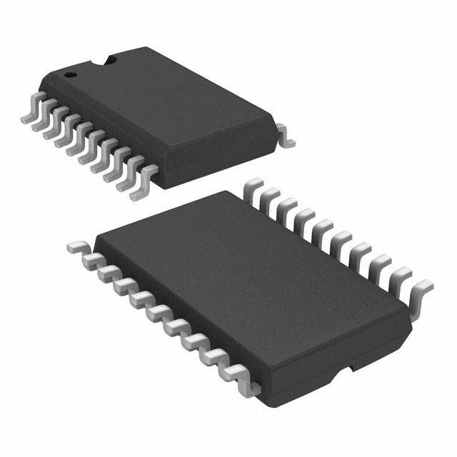
| 描述 | IC 16-BIT SERIAL A/D 20-SOIC模数转换器 - ADC 16-Bit 10us Serial CMOS Sampling |
| 产品分类 | |
| 品牌 | Texas Instruments |
| 产品手册 | http://www.ti.com/litv/sbas017c |
| 产品图片 |
|
| rohs | 符合RoHS无铅 / 符合限制有害物质指令(RoHS)规范要求 |
| 产品系列 | 数据转换器IC,模数转换器 - ADC,Texas Instruments ADS7809UB- |
| 数据手册 | |
| 产品型号 | ADS7809UB |
| 产品培训模块 | http://www.digikey.cn/PTM/IndividualPTM.page?site=cn&lang=zhs&ptm=13240 |
| 产品目录页面 | |
| 产品种类 | 模数转换器 - ADC |
| 位数 | 16 |
| 供应商器件封装 | 20-SOIC |
| 信噪比 | 88 dB |
| 分辨率 | 16 bit |
| 制造商产品页 | http://www.ti.com/general/docs/suppproductinfo.tsp?distId=10&orderablePartNumber=ADS7809UB |
| 包装 | 管件 |
| 单位重量 | 500.700 mg |
| 商标 | Texas Instruments |
| 安装类型 | 表面贴装 |
| 安装风格 | SMD/SMT |
| 封装 | Tube |
| 封装/外壳 | 20-SOIC(0.295",7.50mm 宽) |
| 封装/箱体 | SOIC-20 |
| 工作温度 | -40°C ~ 85°C |
| 工作电源电压 | 4.75 V to 5.25 V |
| 工厂包装数量 | 25 |
| 接口类型 | DSP |
| 数据接口 | DSP,串行 |
| 最大功率耗散 | 100 mW |
| 最大工作温度 | + 85 C |
| 最小工作温度 | - 40 C |
| 标准包装 | 25 |
| 特性 | - |
| 电压参考 | 2.5 V |
| 电压源 | 模拟和数字 |
| 系列 | ADS7809 |
| 结构 | SAR |
| 转换器数 | 1 |
| 转换器数量 | 1 |
| 转换速率 | 100 kS/s |
| 输入数和类型 | 3 个单端,单极3 个单端,双极 |
| 输入类型 | Single-Ended |
| 通道数量 | 1 Channel |
| 配用 | /product-detail/zh/ADS7809EVM/296-17703-ND/716876 |
| 采样率(每秒) | 100k |


- 商务部:美国ITC正式对集成电路等产品启动337调查
- 曝三星4nm工艺存在良率问题 高通将骁龙8 Gen1或转产台积电
- 太阳诱电将投资9.5亿元在常州建新厂生产MLCC 预计2023年完工
- 英特尔发布欧洲新工厂建设计划 深化IDM 2.0 战略
- 台积电先进制程称霸业界 有大客户加持明年业绩稳了
- 达到5530亿美元!SIA预计今年全球半导体销售额将创下新高
- 英特尔拟将自动驾驶子公司Mobileye上市 估值或超500亿美元
- 三星加码芯片和SET,合并消费电子和移动部门,撤换高东真等 CEO
- 三星电子宣布重大人事变动 还合并消费电子和移动部门
- 海关总署:前11个月进口集成电路产品价值2.52万亿元 增长14.8%


PDF Datasheet 数据手册内容提取
ADS7809 ADS7809 SBAS017C – NOVEMBER 1996 – REVISED OCTOBER 2006 µ 16-Bit 10 s Serial CMOS Sampling ANALOG-TO-DIGITAL CONVERTER FEATURES DESCRIPTION (cid:1) 100kHz SAMPLING RATE The ADS7809 is a complete 16-bit sampling Analog-to- (cid:1) 86dB SINAD WITH 20kHz INPUT Digital (A/D) converter using state-of-the-art CMOS struc- (cid:1) ±2LSB INL tures. It contains a 16-bit capacitor-based Successive Ap- proximation Register (SAR) A/D converter with sample-and- (cid:1) DNL: 16 Bits No Missing Codes hold, reference, clock, and a serial data interface. Data can (cid:1) SIX SPECIFIED INPUT RANGES be outputted using the internal clock, or can be synchronized (cid:1) SERIAL OUTPUT to an external data clock. The ADS7809 also provides an output synchronization pulse for ease of use with standard (cid:1) SINGLE +5V SUPPLY OPERATION DSP processors. (cid:1) PIN-COMPATIBLE WITH 12-BIT ADS7808 The ADS7809 is specified at a 100kHz sampling rate, and (cid:1) USES INTERNAL OR EXTERNAL specified over the full temperature range. Laser-trimmed REFERENCE scaling resistors provide various input ranges including ±10V (cid:1) 100mW MAX POWER DISSIPATION and 0V to 5V, while an innovative design operates from a (cid:1) 0.3" SO-20 single +5V supply, with power dissipation under 100mW. (cid:1) SIMPLE DSP INTERFACE The ADS7809 is available in a 0.3" SO-20, and is fully specified for operation over the industrial –40°C to +85°C range. Power R/C CS Down Successive Approximation Register and Control Logic Clock 20kΩ CDAC R1 IN 10kΩ BUSY R2 IN 20kΩ Serial 5kΩ Data Data Clock R3 Comparator IN Out CAP Serial Data Buffer Internal +2.5V Ref 4kΩ REF Please be aware that an important notice concerning availability, standard warranty, and use in critical applications of Texas Instruments semiconductor products and disclaimers thereto appears at the end of this data sheet. All trademarks are the property of their respective owners. PRODUCTION DATA information is current as of publication date. Copyright © 1996-2006, Texas Instruments Incorporated Products conform to specifications per the terms of Texas Instruments standard warranty. Production processing does not necessarily include testing of all parameters. www.ti.com
ABSOLUTE MAXIMUM RATINGS(1) ELECTROSTATIC Analog Inputs: R1IN..........................................................................±25V DISCHARGE SENSITIVITY R2 ..........................................................................±25V IN R3 ..........................................................................±25V REIFN.................................V + 0.3V to AGND2 – 0.3V This integrated circuit can be damaged by ESD. Texas Instru- ANA CAP.......................................Indefinite Short to AGND2, ments recommends that all integrated circuits be handled with .........................................................................Momentary Short to V ANA appropriate precautions. Failure to observe proper handling Ground Voltage Differences: DGND, AGND2.................................±0.3V V ......................................................................................................7V and installation procedures can cause damage. ANA V to V .......................................................................................+0.3 DIG ANA ESD damage can range from subtle performance degrada- V .......................................................................................................7V DDigIGital Inputs............................................................–0.3V to V + 0.3V tion to complete device failure. Precision integrated circuits DIG Maximum Junction Temperature..................................................+165°C may be more susceptible to damage because very small Internal Power Dissipation............................................................700mW parametric changes could cause the device not to meet its Lead Temperature (soldering, 10s)..............................................+300°C published specifications. NOTE: (1) Stresses above those listed under Absolute Maximum Ratings may cause permanent damage to the device. Exposure to absolute maximum conditions for extended periods may affect device reliability. PACKAGE/ORDERING INFORMATION(1) MINIMUM SIGNAL-TO- MAXIMUM NO MISSING (NOISE + SPECIFIED LINEARITY CODE LEVEL DISTORTION) PACKAGE- PACKAGE TEMPERATURE PACKAGE ORDERING TRANSPORT PRODUCT ERROR (LSB) (LSB) RATIO (dB) LEAD DESIGNATOR RANGE MARKING NUMBER MEDIA, QUANTITY ADS7809U ±3 15 83 SO-20 DW –40°C to +85°C ADS7809U ADS7809U Rail, 38 " " " " " " " " ADS7809U/1K Tape and Reel, 1000 ADS7809UB ±2 16 86 " " " ADS7809UB ADS7809UB Rail, 38 " " " " " " " " ADS7809UB/1K Tape and Reel, 1000 NOTE: (1) For the most current package and ordering information, see the Package Option Addendum at the end of this document, or see the TI web site at www.ti.com. ADS7809 2 www.ti.com SBAS017C
ELECTRICAL CHARACTERISTICS At T = –40°C to +85°C, f = 100kHz, V = V = +5V, using internal reference and fixed resistors (see Figure 4), unless otherwise specified. A S DIG ANA ADS7809U ADS7809UB PARAMETER CONDITIONS MIN TYP MAX MIN TYP MAX UNITS RESOLUTION 16 ✻ Bits ANALOG INPUT Voltage Ranges ±10, 0V to 5V, etc. (See Table I) Impedance See Table I Capacitance 35 ✻ pF THROUGHPUT SPEED Complete Cycle Acquire and Convert 10 ✻ µs Throughput Rate 100 ✻ kHz DC ACCURACY Integral Linearity Error ±3 ±2 LSB(1) Differential Linearity Error +3, –2 ±1 LSB No Missing Codes 15 16 Bits Transition Noise(2) 1.3 ✻ LSB Full-Scale Error(3,4) ±0.5 ✻ % Full-Scale Error Drift ±7 ✻ ppm/°C Full-Scale Error(3,4) Ext. 2.5000V Ref ±0.5 ✻ % Full-Scale Error Drift Ext. 2.5000V Ref ±2 ✻ ppm/°C Bipolar Zero Error(3) Bipolar Ranges ±10 ✻ mV Bipolar Zero Error Drift Bipolar Ranges ±2 ✻ ppm/°C Unipolar Zero Error(3) 0V to 10V Ranges ±5 ✻ mV Unipolar Zero Error(3) 0V to 4V, 0V to 5V Ranges ±3 ✻ mV Unipolar Zero Error Drift Unipolar Ranges ±2 ✻ ppm/°C Recovery to Rated Accuracy 1µF Capacitor to CAP 1 ✻ ms after Power-Down Power-Supply Sensitivity +4.75V < V < +5.25V ±8 ✻ LSB D (V = V = V ) DIG ANA D AC ACCURACY Spurious-Free Dynamic Range f = 20kHz 90 100 96 ✻ dB(5) IN Total Harmonic Distortion f = 20kHz –100 –90 ✻ –94 dB IN Signal-to-(Noise + Distortion) f = 20kHz 83 88 86 ✻ dB IN –60dB Input 30 32 dB Signal-to-Noise f = 20kHz 83 88 86 ✻ dB IN Full-Power Bandwidth(6) 250 ✻ kHz SAMPLING DYNAMICS Aperture Delay 40 ✻ ns Transient Response FS Step 2 ✻ µs Overvoltage Recovery(7) 150 ✻ ns REFERENCE Internal Reference Voltage No Load 2.48 2.5 2.52 ✻ ✻ ✻ V Internal Reference Source Current 1 ✻ µA (Must use external buffer) External Reference Voltage Range 2.3 2.5 2.7 ✻ ✻ ✻ V For Specified Linearity External Reference Current Drain Ext. 2.5000V Ref 100 ✻ µA DIGITAL INPUTS Logic Levels V –0.3 +0.8 ✻ ✻ V IL V (8) +2.0 V + 0.3V ✻ ✻ V IH D I V = 0V ±10 ✻ µA IL IL I V = 5V ±10 ✻ µA IH IH ADS7809 3 SBAS017C www.ti.com
ELECTRICAL CHARACTERISTICS (Cont.) At T = –40°C to +85°C, f = 100kHz, V = V = +5V, using internal reference and fixed resistors as shown in Figure 4, unless otherwise specified. A S DIG ANA ADS7809U ADS7809UB PARAMETER CONDITIONS MIN TYP MAX MIN TYP MAX UNITS DIGITAL OUTPUTS Data Format Serial 16 bits Data Co Binary Two’s Complement or Straight Binary Pipeline Delay Conversion results only available after completed conversion. Data Clock Selectable for internal or external data clock Internal EXT/INT LOW 2.3 ✻ MHz (Output Only When Transmitting Data) External EXT/INT HIGH 0.1 10 ✻ ✻ MHz (Can Run Continually) V I = 1.6mA +0.4 ✻ V OL SINK V I = 500µA +4 ✻ V OH SOURCE Leakage Current High-Z State, ±5 ✻ µA V = 0V to V OUT DIG Output Capacitance High-Z State 15 ✻ pF POWER SUPPLIES Specified Performance V Must be ≤ V +4.75 +5 +5.25 ✻ ✻ ✻ V DIG ANA V +4.75 +5 +5.25 ✻ ✻ ✻ V ANA I 0.3 ✻ mA DIG I 16 ✻ mA ANA Power Dissipation: PWRD LOW V = V = 5V, f = 100kHz 100 ✻ mW ANA DIG S PWRD HIGH 50 ✻ µW TEMPERATURE RANGE Specified Performance –40 +85 ✻ ✻ °C Derated Performance –55 +125 ✻ ✻ °C Storage –65 +150 ✻ ✻ °C Thermal Resistance (θ ) JA SO 75 ✻ °C/W ✻ Same as specification for ADS7809U. NOTES:(1) LSB means Least Significant Bit. For the ±10V input range, one LSB is 305µV. (2) Typical rms noise at worst case transitions and temperatures. (3) As measured with fixed resistors shown in Figure 4. Adjustable to zero with external potentiometer. (4) For bipolar input ranges, full-scale error is the worst case of –Full Scale or +Full Scale untrimmed deviation from ideal first and last code transitions, divided by the transition voltage (not divided by the full-scale range) and includes the effect of offset error. For unipolar input ranges, full-scale error is the deviation of the last code transition divided by the transition voltage. It also includes the effect of offset error. (5) All specifications in dB are referred to a full-scale ±10V input. (6) Full-Power Bandwidth defined as Full-Scale input frequency at which Signal-to-(Noise + Distortion) degrades to 60dB. (7) Recovers to specified performance after 2 • FS input overvoltage. (8) The minimum V level for the DATACLK signal is 3V. IH ADS7809 4 www.ti.com SBAS017C
PIN ASSIGNMENTS PIN # NAME DESCRIPTION 1 R1 Analog Input. See Table I and Figure 4 for input range connections. IN 2 AGND1 Analog Ground. Used internally as ground reference point. Minimal current flow. 3 R2 Analog Input. See Table I and Figure 4 for input range connections. IN 4 R3 Analog Input. See Table I and Figure 4 for input range connections. IN 5 CAP Reference Buffer Capacitor. 2.2µF Tantalum to ground. 6 REF Reference Input/Output. Outputs internal 2.5V reference. Can also be driven by external system reference. In both cases, bypass to ground with a 2.2µF Tantalum capacitor. 7 AGND2 Analog Ground 8 SB/BTC Select Straight Binary or Binary Two’s Complement data output format. If HIGH, data will be output in a Straight Binary format. If LOW, data will be output in a Binary Two’s Complement format. 9 EXT/INT Select External or Internal Clock for transmitting data. If HIGH, data will be output synchronized to the clock input on DATACLK. If LOW, a convert command will initiate the transmission of the data from the previous conversion, along with 16 clock pulses output on DATACLK. 10 DGND Digital Ground 11 SYNC Synch Output. If EXT/INT is HIGH, either a rising edge on R/C with CS LOW or a falling edge on CS with R/C HIGH will output a pulse on SYNC synchronized to the external DATACLK. 12 DATACLK Either an input or an output depending on the EXT/INT level. Output data will be synchronized to this clock. If EXT/INT is LOW, DATACLK will transmit 16 pulses after each conversion, and then remain LOW between conversions. 13 DATA Serial Data Output. Data will be synchronized to DATACLK, with the format determined by the level of SB/BTC. In the external clock mode, after 16 bits of data, the ADS7809 will output the level input on TAG as long as CS is LOW and R/C is HIGH (see Figure 3). If EXT/INT is LOW, data will be valid on both the rising and falling edges of DATACLK, and between conversions DATA will stay at the level of the TAG input when the conversion was started. 14 TAG Tag Input for use in external clock mode. If EXT/INT is HIGH, digital data input on TAG will be output on DATA with a delay of 16 DATACLK pulses as long as CS is LOW and R/C is HIGH. See Figure 3. 15 R/C Read/Convert Input. With CS LOW, a falling edge on R/C puts the internal sample-and-hold into the hold state and starts a conversion. When EXT/INT is LOW, this also initiates the transmission of the data results from the previous conversion. If EXT/INT is HIGH, a rising edge on R/C with CS LOW, or a falling edge on CS with R/C HIGH, transmits a pulse on SYNC and initiates the transmission of data from the previous conversion. 16 CS Chip Select. Internally OR’ed with R/C. 17 BUSY Busy Output. Falls when a conversion is started, and remains LOW until the conversion is completed and the data is latched into the output shift register. CS or R/C must be HIGH when BUSY rises, or another conversion will start without time for signal acquisition. 18 PWRD Power Down Input. If HIGH, conversions are inhibited and power consumption is significantly reduced. Results from the previous conversion are maintained in the output shift register. 19 V Analog Supply Input. Nominally +5V. Connect directly to pin 20, and decouple to ground with 0.1µF ceramic and 10µF tantalum ANA capacitors. 20 V Digital Supply Input. Nominally +5V. Connect directly to pin 19. Must be ≤ V . DIG ANA PIN CONFIGURATION ANALOG CONNECT R1 CONNECT R2 IN IN INPUT VIA 200Ω VIA 100Ω CONNECT R3 IN RANGE TO TO TO IMPEDANCE ±10V V AGND CAP 22.9kΩ IN ±5V AGND V CAP 13.3kΩ IN R1IN 1 20 VDIG 0V±3 t.o3 31V0V AGVINND VVIN ACGANPD 1103..73kkΩΩ IN AGND1 2 19 V 0V to 5V AGND AGND V 10.0kΩ ANA IN 0V to 4V V AGND V 10.7kΩ IN IN R2 3 18 PWRD IN TABLE I. Input Range Connections. See Figure 4 for complete R3 4 17 BUSY IN information. CAP 5 ADS7809 16 CS REF 6 15 R/C t 1 CS, R/C AGND2 7 14 TAG SB/BTC 8 13 DATA BUSY t3 t t 2 4 EXT/INT 9 12 DATACLK t 5 DGND 10 11 SYNC MODE Acquire Convert Acquire t t 6 7 FIGURE 1. Basic Conversion Timing. ADS7809 5 SBAS017C www.ti.com
SYMBOL DESCRIPTION MIN TYP MAX UNITS t Convert Pulse Width 40 6000 ns 1 t BUSY Delay 65 ns 2 t BUSY LOW 8 µs 3 t BUSY Delay After End of Conversion 220 ns 4 t Aperture Delay 40 ns 5 t Conversion Time 7.6 8 µs 6 t Acquisition Time 2 µs 7 t + t Throughput Time 9 10 µs 6 7 t R/C LOW to DATACLK Delay 450 ns 8 t DATACLK Period 440 ns 9 t Data Valid to DATACLK HIGH Delay 20 75 ns 10 t Data Valid After DATACLK LOW Delay 100 125 ns 11 t External DATACLK 100 ns 12 t External DATACLK HIGH 20 ns 13 t External DATACLK LOW 30 ns 14 t DATACLK HIGH Setup Time 20 t + 5 ns 15 12 t R/C to CS Setup Time 10 ns 16 t SYNC Delay After DATACLK HIGH 15 35 ns 17 t Data Valid Delay 25 55 ns 18 t CS to Rising Edge Delay 25 ns 19 t Data Available after CS LOW 6 µs 20 TABLE II. Conversion and Data Timing. T = –40°C to +85°C. A t 8 R/C t t 9 1 DATACLK 1 2 3 15 16 t 11 t 10 SDATA MSB Valid Bit 14 Valid Bit 13 Valid Bit 1 Valid LSB Valid t 2 t 3 BUSY FIGURE 2. Serial Data Timing Using Internal Clock. (CS, EXT/INT and TAG Tied LOW.) ADS7809 6 www.ti.com SBAS017C
SPECIFIC FUNCTION CS R/C BUSY EXT/INT DATACLK PWRD SB/BTC OPERATION Initiate Conversion and 1 > 0 0 1 0 Output 0 x Initiates conversion “n”. Data from conversion “n – 1” Output Data Using clocked out on DATA synchronized to 16 clock Internal Clock pulses output on DATACLK. 0 1 > 0 1 0 Output 0 x Initiates conversion “n”. Data from conversion “n – 1” clocked out on DATA synchronized to 16 clock pulses output on DATACLK. Initiate Conversion and 1 > 0 0 1 1 Input 0 x Initiates conversion “n”. Output Data Using External 0 1 > 0 1 1 Input 0 x Initiates conversion “n”. Clock 1 > 0 1 1 1 Input x x Outputs a pulse on SYNC followed by data from conversion “n” clocked out synchronized to external DATACLK. 1 > 0 1 0 1 Input 0 x Outputs a pulse on SYNC followed by data from conversion “n – 1” clocked out synchronized to external DATACLK.(1) Conversion “n” in process. 0 0 > 1 0 1 Input 0 x Outputs a pulse on SYNC followed by data from conversion “n – 1” clocked out synchronized to external DATACLK .(1) Conversion “n” in process. Incorrect Conversions 0 0 0 > 1 x x 0 x CS or R/C must be HIGH or a new conversion will be initiated without time for acquisition. Power-Down x x x x x 0 x Analog circuitry powered. Conversion can proceed. x x x x x 1 x Analog circuitry disabled. Data from previous conversion maintained in output registers. Selecting Output Format x x x x x x 0 Serial data is output in Binary Two’s Complement format. x x x x x x 1 Serial data is output in Straight Binary format. NOTE: (1) See Figure 3b for constraints on previous data valid during conversion. TABLE III. Control Truth Table. DIGITAL OUTPUT BINARY TWO’S COMPLEMENT STRAIGHT BINARY (SB/BTC LOW) (SB/BTC HIGH) HEX HEX DESCRIPTION ANALOG INPUT BINARY CODE CODE BINARY CODE CODE Full-Scale Range ±10 ±5 ±3.33V 0V to 10V 0V to 5V 0V to 4V Least Significant Bit (LSB) 305µV 153µV 102µV 153µV 76µV 61µV +Full Scale (FS – 1LSB) 9.999695V 4.999847V 3.333231V 9.999847V 4.999924V 3.999939V 0111 1111 1111 1111 7FFF 1111 1111 1111 1111 FFFF Midscale 0V 0V 0V 5V 2.5V 2V 0000 0000 0000 0000 0000 1000 0000 0000 0000 8000 One LSB Below Midscale –305µV –153µV –102µV 4.999847V 2.499924V 1.999939V 1111 1111 1111 1111 FFFF 0111 1111 1111 1111 7FFF –Full Scale –10V –5V –3.333333V 0V 0V 0V 1000 0000 0000 0000 8000 0000 0000 0000 0000 0000 TABLE IV. Output Codes and Ideal Input Voltages. ADS7809 7 SBAS017C www.ti.com
8 F IG U R E 3 a . C o n v e rs io n a n d R t13 t12 t14 e a 0 1 2 3 4 13 14 d T EXTERNAL im DATACLK in g w t1 t15 t19 ith CS E x t16 te rn w al C R/C ww loc t2 t16 .ti.c k. ( BUSY t17 o E m X T /IN SYNC t12 T T t18 ie d DATA Bit 15 (MSB) Bit 14 Bit 1 Bit 0 (LSB) Tag 0 Tag 1 H ig h .) R TAG Tag 0 Tag 1 Tag 2 Tag 15 Tag 16 Tag 17 Tag 18 Tag 19 e a d A fte r C o n v e rs io n . A SD B AS S 07 178 C0 9
9 1 g a T Tag 1 Tag 18 t19 7 0 1 g g a a T T B) S 6 L 1 0 ( ag Bit T B) t20 MS g 1 5 ( Ta 1 Bit t18 t12 0 g a T t15 t17 t14 t1 t12 t13 t2 t16 NALCLK CS R/C USY YNC ATA TAG RA B S D ET TA XD E FIGURE 3b. Conversion and Read Timing with External Clock. (EXT/INT Tied High.) Read During Conversion (Previous Conversion Results). ADS7809 9 SBAS017C www.ti.com
With Trim Input Range Without Trim (Adjust offset first at 0V, then adjust gain) 200Ω 200Ω R1IN R1IN AGND1 AGND1 100Ω 100Ω VIN R2IN 33.2kΩ VIN R2IN 0V-10V 33.2kΩ R3IN R3IN +5V 2.2µF + CAP +5V CAP 2.2µF + 50kΩ 576kΩ REF 50kΩ REF + + 2.2µF 2.2µF AGND2 AGND2 200Ω 200Ω R1IN R1IN AGND1 AGND1 100Ω 100Ω 33.2kΩ R2IN 33.2kΩ R2IN VIN R3IN VIN R3IN +5V 0V-5V CAP CAP + +5V 2.2µF REF 50kΩ 2.2µF + 50kΩ 576kΩ REF + + 2.2µF 2.2µF AGND2 AGND2 200Ω 200Ω V R1 V R1 IN IN IN IN AGND1 AGND1 100Ω 100Ω R2IN R2IN R3IN R3IN 33.2kΩ 33.2kΩ +5V + CAP +5V + CAP 0V-4V 2.2µF 2.2µF 576kΩ REF 50kΩ 50kΩ REF + + 2.2µF 2.2µF AGND2 AGND2 FIGURE 4a. Offset/Gain Circuits for Unipolar Input Ranges. ADS7809 10 www.ti.com SBAS017C
With Trim Input Range Without Trim (Adjust offset first at 0V, then adjust gain) 200Ω 200Ω VIN R1IN VIN R1IN AGND1 AGND1 100Ω 100Ω R2IN R2IN ±10V +5V 33.2kΩ R3IN 33.2kΩ R3IN 50kΩ + CAP +5V + CAP 2.2µF 2.2µF 576kΩ REF REF 50kΩ 2.2µF+ 2.2µF+ AGND2 AGND2 200Ω 200Ω R1IN R1IN AGND1 AGND1 100Ω 100Ω 33.2kΩ VIN R2IN VIN R2IN 33.2kΩ R3 R3 IN + IN ± 5V +5V 2.2µF CAP +5V CAP + 2.2µF 50kΩ 576kΩ REF 50kΩ REF 2.2µF + 2.2µF + AGND2 AGND2 200Ω 200Ω VIN R1IN VIN R1IN 100Ω AGND1 100Ω AGND1 R2IN R2IN 33.2kΩ R3IN 33.2kΩ R3IN + +5V 2.2µF CAP CAP +5V ±3.3V 50kΩ 576kΩ + 2.2µF REF 50kΩ REF +2.2µF +2.2µF AGND2 AGND2 FIGURE 4b. Offset/Gain Circuits for Bipolar Input Ranges. ADS7809 11 SBAS017C www.ti.com
Revision History DATE REVISION PAGE SECTION DESCRIPTION 10/06 C 3 Absolute Maximum Ratings CAP and REF were switched. NOTE: Page numbers for previous revisions may differ from page numbers in the current version. ADS7809 12 www.ti.com SBAS017C
PACKAGE OPTION ADDENDUM www.ti.com 6-Feb-2020 PACKAGING INFORMATION Orderable Device Status Package Type Package Pins Package Eco Plan Lead/Ball Finish MSL Peak Temp Op Temp (°C) Device Marking Samples (1) Drawing Qty (2) (6) (3) (4/5) ADS7809U ACTIVE SOIC DW 20 25 Green (RoHS NIPDAU-DCC Level-3-260C-168 HR -40 to 85 ADS7809U & no Sb/Br) ADS7809U/1K ACTIVE SOIC DW 20 1000 Green (RoHS NIPDAU-DCC Level-3-260C-168 HR -40 to 85 ADS7809U & no Sb/Br) ADS7809U/1KE4 ACTIVE SOIC DW 20 1000 Green (RoHS NIPDAU-DCC Level-3-260C-168 HR -40 to 85 ADS7809U & no Sb/Br) ADS7809UB ACTIVE SOIC DW 20 25 Green (RoHS NIPDAU-DCC Level-3-260C-168 HR -40 to 85 ADS7809U & no Sb/Br) B ADS7809UB/1K ACTIVE SOIC DW 20 1000 Green (RoHS NIPDAU-DCC Level-3-260C-168 HR -40 to 85 ADS7809U & no Sb/Br) B ADS7809UE4 ACTIVE SOIC DW 20 25 Green (RoHS NIPDAU-DCC Level-3-260C-168 HR -40 to 85 ADS7809U & no Sb/Br) (1) The marketing status values are defined as follows: ACTIVE: Product device recommended for new designs. LIFEBUY: TI has announced that the device will be discontinued, and a lifetime-buy period is in effect. NRND: Not recommended for new designs. Device is in production to support existing customers, but TI does not recommend using this part in a new design. PREVIEW: Device has been announced but is not in production. Samples may or may not be available. OBSOLETE: TI has discontinued the production of the device. (2) RoHS: TI defines "RoHS" to mean semiconductor products that are compliant with the current EU RoHS requirements for all 10 RoHS substances, including the requirement that RoHS substance do not exceed 0.1% by weight in homogeneous materials. Where designed to be soldered at high temperatures, "RoHS" products are suitable for use in specified lead-free processes. TI may reference these types of products as "Pb-Free". RoHS Exempt: TI defines "RoHS Exempt" to mean products that contain lead but are compliant with EU RoHS pursuant to a specific EU RoHS exemption. Green: TI defines "Green" to mean the content of Chlorine (Cl) and Bromine (Br) based flame retardants meet JS709B low halogen requirements of <=1000ppm threshold. Antimony trioxide based flame retardants must also meet the <=1000ppm threshold requirement. (3) MSL, Peak Temp. - The Moisture Sensitivity Level rating according to the JEDEC industry standard classifications, and peak solder temperature. (4) There may be additional marking, which relates to the logo, the lot trace code information, or the environmental category on the device. (5) Multiple Device Markings will be inside parentheses. Only one Device Marking contained in parentheses and separated by a "~" will appear on a device. If a line is indented then it is a continuation of the previous line and the two combined represent the entire Device Marking for that device. Addendum-Page 1
PACKAGE OPTION ADDENDUM www.ti.com 6-Feb-2020 (6) Lead/Ball Finish - Orderable Devices may have multiple material finish options. Finish options are separated by a vertical ruled line. Lead/Ball Finish values may wrap to two lines if the finish value exceeds the maximum column width. Important Information and Disclaimer:The information provided on this page represents TI's knowledge and belief as of the date that it is provided. TI bases its knowledge and belief on information provided by third parties, and makes no representation or warranty as to the accuracy of such information. Efforts are underway to better integrate information from third parties. TI has taken and continues to take reasonable steps to provide representative and accurate information but may not have conducted destructive testing or chemical analysis on incoming materials and chemicals. TI and TI suppliers consider certain information to be proprietary, and thus CAS numbers and other limited information may not be available for release. In no event shall TI's liability arising out of such information exceed the total purchase price of the TI part(s) at issue in this document sold by TI to Customer on an annual basis. Addendum-Page 2
PACKAGE MATERIALS INFORMATION www.ti.com 24-Jul-2013 TAPE AND REEL INFORMATION *Alldimensionsarenominal Device Package Package Pins SPQ Reel Reel A0 B0 K0 P1 W Pin1 Type Drawing Diameter Width (mm) (mm) (mm) (mm) (mm) Quadrant (mm) W1(mm) ADS7809U/1K SOIC DW 20 1000 330.0 24.4 10.8 13.3 2.7 12.0 24.0 Q1 ADS7809UB/1K SOIC DW 20 1000 330.0 24.4 10.8 13.3 2.7 12.0 24.0 Q1 PackMaterials-Page1
PACKAGE MATERIALS INFORMATION www.ti.com 24-Jul-2013 *Alldimensionsarenominal Device PackageType PackageDrawing Pins SPQ Length(mm) Width(mm) Height(mm) ADS7809U/1K SOIC DW 20 1000 367.0 367.0 45.0 ADS7809UB/1K SOIC DW 20 1000 367.0 367.0 45.0 PackMaterials-Page2
PACKAGE OUTLINE DW0020A SOIC - 2.65 mm max height SCALE 1.200 SOIC C 10.63 SEATING PLANE TYP 9.97 A PIN 1 ID 0.1 C AREA 18X 1.27 20 1 13.0 2X 12.6 11.43 NOTE 3 10 11 0.51 20X 7.6 0.31 2.65 MAX B 7.4 0.25 C A B NOTE 4 0.33 TYP 0.10 0.25 SEE DETAIL A GAGE PLANE 0.3 1.27 0 - 8 0.1 0.40 DETAIL A TYPICAL 4220724/A 05/2016 NOTES: 1. All linear dimensions are in millimeters. Dimensions in parenthesis are for reference only. Dimensioning and tolerancing per ASME Y14.5M. 2. This drawing is subject to change without notice. 3. This dimension does not include mold flash, protrusions, or gate burrs. Mold flash, protrusions, or gate burrs shall not exceed 0.15 mm per side. 4. This dimension does not include interlead flash. Interlead flash shall not exceed 0.43 mm per side. 5. Reference JEDEC registration MS-013. www.ti.com
EXAMPLE BOARD LAYOUT DW0020A SOIC - 2.65 mm max height SOIC 20X (2) SYMM 1 20 20X (0.6) 18X (1.27) SYMM (R0.05) TYP 10 11 (9.3) LAND PATTERN EXAMPLE SCALE:6X SOOPLEDNEINRG MASK METAL MSOELTDAEL RU NMDAESRK SOOPLEDNEINRG MASK 0.07 MAX 0.07 MIN ALL AROUND ALL AROUND NON SOLDER MASK SOLDER MASK DEFINED DEFINED SOLDER MASK DETAILS 4220724/A 05/2016 NOTES: (continued) 6. Publication IPC-7351 may have alternate designs. 7. Solder mask tolerances between and around signal pads can vary based on board fabrication site. www.ti.com
EXAMPLE STENCIL DESIGN DW0020A SOIC - 2.65 mm max height SOIC 20X (2) SYMM 1 20 20X (0.6) 18X (1.27) SYMM 10 11 (9.3) SOLDER PASTE EXAMPLE BASED ON 0.125 mm THICK STENCIL SCALE:6X 4220724/A 05/2016 NOTES: (continued) 8. Laser cutting apertures with trapezoidal walls and rounded corners may offer better paste release. IPC-7525 may have alternate design recommendations. 9. Board assembly site may have different recommendations for stencil design. www.ti.com
IMPORTANTNOTICEANDDISCLAIMER TI PROVIDES TECHNICAL AND RELIABILITY DATA (INCLUDING DATASHEETS), DESIGN RESOURCES (INCLUDING REFERENCE DESIGNS), APPLICATION OR OTHER DESIGN ADVICE, WEB TOOLS, SAFETY INFORMATION, AND OTHER RESOURCES “AS IS” AND WITH ALL FAULTS, AND DISCLAIMS ALL WARRANTIES, EXPRESS AND IMPLIED, INCLUDING WITHOUT LIMITATION ANY IMPLIED WARRANTIES OF MERCHANTABILITY, FITNESS FOR A PARTICULAR PURPOSE OR NON-INFRINGEMENT OF THIRD PARTY INTELLECTUAL PROPERTY RIGHTS. These resources are intended for skilled developers designing with TI products. You are solely responsible for (1) selecting the appropriate TI products for your application, (2) designing, validating and testing your application, and (3) ensuring your application meets applicable standards, and any other safety, security, or other requirements. These resources are subject to change without notice. TI grants you permission to use these resources only for development of an application that uses the TI products described in the resource. Other reproduction and display of these resources is prohibited. No license is granted to any other TI intellectual property right or to any third party intellectual property right. TI disclaims responsibility for, and you will fully indemnify TI and its representatives against, any claims, damages, costs, losses, and liabilities arising out of your use of these resources. TI’s products are provided subject to TI’s Terms of Sale (www.ti.com/legal/termsofsale.html) or other applicable terms available either on ti.com or provided in conjunction with such TI products. TI’s provision of these resources does not expand or otherwise alter TI’s applicable warranties or warranty disclaimers for TI products. Mailing Address: Texas Instruments, Post Office Box 655303, Dallas, Texas 75265 Copyright © 2020, Texas Instruments Incorporated