ICGOO在线商城 > 集成电路(IC) > 数据采集 - 模数转换器 > ADS1148IPW
 Datasheet下载
- 型号: ADS1148IPW
- 制造商: Texas Instruments
- 库位|库存: xxxx|xxxx
- 要求:
| 数量阶梯 | 香港交货 | 国内含税 |
| +xxxx | $xxxx | ¥xxxx |
查看当月历史价格
查看今年历史价格
ADS1148IPW产品简介:
ICGOO电子元器件商城为您提供ADS1148IPW由Texas Instruments设计生产,在icgoo商城现货销售,并且可以通过原厂、代理商等渠道进行代购。 ADS1148IPW价格参考。Texas InstrumentsADS1148IPW封装/规格:数据采集 - 模数转换器, 16 Bit Analog to Digital Converter 4, 7 Input 1 Sigma-Delta 28-TSSOP。您可以下载ADS1148IPW参考资料、Datasheet数据手册功能说明书,资料中有ADS1148IPW 详细功能的应用电路图电压和使用方法及教程。
| 参数 | 数值 |
| 产品目录 | 集成电路 (IC)半导体 |
| 描述 | IC ADC 16BIT SRL 2KSPS 28TSSOP模数转换器 - ADC 16B ADC For Temp Sensors |
| 产品分类 | |
| 品牌 | Texas Instruments |
| 产品手册 | |
| 产品图片 |
|
| rohs | 符合RoHS无铅 / 符合限制有害物质指令(RoHS)规范要求 |
| 产品系列 | 数据转换器IC,模数转换器 - ADC,Texas Instruments ADS1148IPW- |
| 数据手册 | |
| 产品型号 | ADS1148IPW |
| 产品种类 | 模数转换器 - ADC |
| 位数 | 16 |
| 供应商器件封装 | 28-TSSOP |
| 信噪比 | Yes |
| 其它名称 | 296-27417-5 |
| 分辨率 | 16 bit |
| 包装 | 管件 |
| 商标 | Texas Instruments |
| 安装类型 | 表面贴装 |
| 安装风格 | SMD/SMT |
| 封装 | Tube |
| 封装/外壳 | 28-TSSOP(0.173",4.40mm 宽) |
| 封装/箱体 | TSSOP-28 |
| 工作温度 | -40°C ~ 125°C |
| 工作电源电压 | 2.7 V to 5.25 V |
| 工厂包装数量 | 50 |
| 接口类型 | Serial (SPI) |
| 数据接口 | SPI |
| 最大功率耗散 | 2.3 mW |
| 最大工作温度 | + 125 C |
| 最小工作温度 | - 40 C |
| 标准包装 | 50 |
| 特性 | PGA, 温度传感器 |
| 电压参考 | Internal, External |
| 电压源 | 模拟和数字,双 ± |
| 系列 | ADS1148 |
| 结构 | Sigma-Delta |
| 转换器数 | 1 |
| 转换器数量 | 1 |
| 转换速率 | 2 kS/s |
| 输入数和类型 | 7 个单端,单极7 个单端,双极4 个差分,单极4 个差分,双极 |
| 输入类型 | Single-Ended/Differential |
| 通道数量 | 3 Channel/2 Channel |
| 采样率(每秒) | 5 ~ 2k |


- 商务部:美国ITC正式对集成电路等产品启动337调查
- 曝三星4nm工艺存在良率问题 高通将骁龙8 Gen1或转产台积电
- 太阳诱电将投资9.5亿元在常州建新厂生产MLCC 预计2023年完工
- 英特尔发布欧洲新工厂建设计划 深化IDM 2.0 战略
- 台积电先进制程称霸业界 有大客户加持明年业绩稳了
- 达到5530亿美元!SIA预计今年全球半导体销售额将创下新高
- 英特尔拟将自动驾驶子公司Mobileye上市 估值或超500亿美元
- 三星加码芯片和SET,合并消费电子和移动部门,撤换高东真等 CEO
- 三星电子宣布重大人事变动 还合并消费电子和移动部门
- 海关总署:前11个月进口集成电路产品价值2.52万亿元 增长14.8%


PDF Datasheet 数据手册内容提取
Product Sample & Technical Tools & Support & Folder Buy Documents Software Community ADS1146,ADS1147,ADS1148 SBAS453G–JULY2009–REVISEDAUGUST2016 ADS114x 16-Bit, 2-kSPS, Analog-to-Digital Converters With Programmable Gain Amplifier (PGA) for Sensor Measurement 1 Features 3 Description • ProgrammableDataRatesUpto2kSPS The ADS1146, ADS1147, and ADS1148 devices are 1 precision, 16-bit analog-to-digital converters (ADCs) • Single-CycleSettlingforAllDataRates that include many integrated features to reduce • Simultaneous50-Hzand60-HzRejectionat system cost and component count for sensor 20SPS measurement applications. The devices feature a • AnalogMultiplexerWith8(ADS1148)and low-noise, programmable gain amplifier (PGA), a precision delta-sigma (ΔΣ) ADC with a single-cycle 4(ADS1147)IndependentlySelectableInputs settling digital filter, and an internal oscillator. The • ProgrammableGain:1V/Vto128V/V ADS1147 and ADS1148 devices also provide a built- • Dual-MatchedProgrammableExcitationCurrent in, low-drift voltage reference, and two matched Sources programmableexcitationcurrentsources(IDACs). • Low-DriftInternal2.048-VReference An input multiplexer supports four differential inputs • SensorBurnoutDetection for the ADS1148, two for the ADS1147, and one for the ADS1146. In addition, the multiplexer integrates • 4or8General-PurposeI/Os(ADS1147and sensor burn-out detection, voltage bias for ADS1148) thermocouples, system monitoring, and general • InternalTemperatureSensor purpose digital I/Os (ADS1147 and ADS1148). The • PowerSupplyandV Monitoring(ADS1147and PGA provides selectable gains up to 128 V/V. These REF ADS1148) features provide a complete front-end solution for temperature sensor measurement applications • SelfandSystemCalibration including thermocouples, thermistors, and resistance • SPI™-CompatibleSerialInterface temperature detectors (RTDs) and other small signal • AnalogSupply:Unipolar(2.7Vto5.25V)or measurements including resistive bridge sensors. Bipolar(±2.5V) The digital filter settles in a single cycle to support fast channel cycling when using the input multiplexer • DigitalSupply:2.7Vto5.25V and provides data rates up to 2 kSPS. For data rates of 20 SPS or less, both 50-Hz and 60-Hz interference 2 Applications arerejectedbythefilter. • TemperatureMeasurement DeviceInformation(1) – RTDs,Thermocouples,andThermistors • PressureMeasurement PARTNUMBER PACKAGE BODYSIZE(NOM) ADS1146 TSSOP(16) 5.00mm×4.40mm • FlowMeters ADS1147 TSSOP(20) 6.50mm×4.40mm • FactoryAutomationandProcessControl TSSOP(28) 9.70mm×4.40mm ADS1148 VQFN(32) 5.00mm×5.00mm (1) For all available packages, see the orderable addendum at theendofthedatasheet. FunctionalBlockDiagrams ADS1148 REFP0/REFN0/ Only AVDD REFP REFN DVDD AVDD GPIO0 GPIO1 REFP1REFN1VREFOUTVREFCOM DVDD VBBDIuAeSrnteocutt ADS1146 VBIASBDuernteocutt VREF Mux RVefoeltraegnece AADDSS11114478 GPIO SCLK AIN0/IEXC System SCLK DIN AIN1/IEXC Monitor DIN AAIINNPN IMnpuuxt PGA M3rodd ßOu(cid:8)lra(cid:3)d(cid:3)teorr AdDjFuiigsltitetaarblle InCStAoeenrnrftiadraoclel DDCORSDUYT/DRDY AAAIIINNN234///IIIEEEXXXCCC///GGGPPPIIIOOO234 IMnpuuxt PGA M3rodd ßOu(cid:8)lra(cid:3)d(cid:3)teorr AdDjFuiigsltitetaarblle InCStAoeenrnrftiadaroclel DCDORSUDTY/DRDY START AIN5/IEXC/GPIO5 START OInstceilrlnaatol r RESET AAIINN67//IIEEXXCC//GGPPIIOO67 DIDuAaCls OInstceilrlnaatol r RESET ADS1148 Only Burnout Burnout Detect Detect AVSS CLK DGND AVSS IEXC1IEXC2 CLK DGND ADS1148 Only Copyright ' 2016, Texas Instruments Incorporated 1 An IMPORTANT NOTICE at the end of this data sheet addresses availability, warranty, changes, use in safety-critical applications, intellectualpropertymattersandotherimportantdisclaimers.PRODUCTIONDATA.
ADS1146,ADS1147,ADS1148 SBAS453G–JULY2009–REVISEDAUGUST2016 www.ti.com Table of Contents 1 Features.................................................................. 1 9.5 Programming...........................................................33 2 Applications........................................................... 1 9.6 RegisterMaps.........................................................42 3 Description............................................................. 1 10 ApplicationandImplementation........................ 62 4 RevisionHistory..................................................... 2 10.1 ApplicationInformation..........................................62 10.2 TypicalApplications..............................................68 5 DeviceComparisonTable..................................... 4 10.3 Do'sandDon'ts.....................................................78 6 PinConfigurationandFunctions......................... 5 11 PowerSupplyRecommendations..................... 80 7 Specifications......................................................... 7 11.1 PowerSupplySequencing....................................80 7.1 AbsoluteMaximumRatings......................................7 11.2 PowerSupplyDecoupling.....................................80 7.2 ESDRatings..............................................................7 12 Layout................................................................... 81 7.3 RecommendedOperatingConditions.......................8 12.1 LayoutGuidelines.................................................81 7.4 ThermalInformation..................................................8 12.2 LayoutExample....................................................82 7.5 ElectricalCharacteristics...........................................9 13 DeviceandDocumentationSupport................. 83 7.6 TimingRequirements..............................................11 7.7 SwitchingCharacteristics........................................11 13.1 DocumentationSupport........................................83 7.8 TypicalCharacteristics............................................13 13.2 RelatedLinks........................................................83 13.3 ReceivingNotificationofDocumentationUpdates83 8 ParameterMeasurementInformation................15 13.4 CommunityResources..........................................83 8.1 NoisePerformance.................................................15 13.5 Trademarks...........................................................83 9 DetailedDescription............................................ 16 13.6 ElectrostaticDischargeCaution............................83 9.1 Overview.................................................................16 13.7 Glossary................................................................83 9.2 FunctionalBlockDiagrams.....................................16 14 Mechanical,Packaging,andOrderable 9.3 FeatureDescription.................................................17 Information........................................................... 84 9.4 DeviceFunctionalModes........................................28 4 Revision History NOTE:Pagenumbersforpreviousrevisionsmaydifferfrompagenumbersinthecurrentversion. ChangesfromRevisionF(April2012)toRevisionG Page • AddedESDRatingstableandFeatureDescription,DeviceFunctionalModes,Applicationand Implementation,PowerSupplyRecommendations,Layout,DeviceandDocumentationSupport,andMechanical, Packaging,andOrderableInformationsections..................................................................................................................... 1 • UpdatedFeaturesandDescriptionsectionstoincludeuseinapplicationsotherthantemperaturemeasurement..............1 • MergedallPinFunctionsintoonetable................................................................................................................................. 6 • ChangedvaluesintheThermalInformationtabletoalignwithJEDECstandards................................................................ 8 • AddedAbsoluteinputcurrentspecificationtoElectricalCharacteristics................................................................................ 9 • ChangedcompliancevoltageforexcitationcurrentsourcesinElectricalCharacteristics,nowreferstoFigure9and Figure10;changedinitialerrorandinitialmismatchtoabsoluteerrorandabsolutemismatch............................................ 9 • ChangedIDACmismatchspecificationinElectricalCharacteristicstabletoreflectproperdistribution................................ 9 • Re-orderedelementsinTimingRequirementstables,changedtimingreferencestot ................................................... 11 CLK • ChangedLow-NoisePGAsection........................................................................................................................................ 18 • ModifiedFigure20toshowvariableresistorposition ......................................................................................................... 18 • Addedf /f columntoTable5....................................................................................................................................... 22 CLK MOD • ChangedChipSelect(CS)section....................................................................................................................................... 33 • ChangedDataOutputandDataReady(DOUT/DRDY)section.......................................................................................... 34 • ChangedFigure42,43,and44............................................................................................................................................ 35 • AddedmoreinfomationtoDataFormatsection;addedFigure45...................................................................................... 36 • ModifiedFigure46toincludeCSstatusthroughSLEEPandWAKEUPcommand............................................................ 38 • UpdatedFigure47andFigure48toshowstartofcommandexecution............................................................................. 38 • RemovedfigureforSDATAC(0001011x)(StopReadDataContinuous)command.......................................................... 40 • UpdatedFigure53toshowMUX1asthestartofthedatabyteforthegivencommandandregisterlocation................... 40 2 SubmitDocumentationFeedback Copyright©2009–2016,TexasInstrumentsIncorporated ProductFolderLinks:ADS1146 ADS1147 ADS1148
ADS1146,ADS1147,ADS1148 www.ti.com SBAS453G–JULY2009–REVISEDAUGUST2016 Revision History (continued) • UpdatedFigure54toshowstartofcalibrationtiming.......................................................................................................... 41 • UpdatedFigure79andFigure80tobettershowtiminginformation................................................................................... 66 ChangesfromRevisionE(April2012)toRevisionF Page • AddedADS1148,QFN-32rowtoPackage/OrderingInformationtable................................................................................. 4 ChangesfromRevisionD(October2011)toRevisionE Page • AddedRHBpinconfiguration................................................................................................................................................. 5 ChangesfromRevisionC(April2010)toRevisionD Page • AddedfootnotetoAnalogInputs,Full-scaleinputvoltageparametertypicalspecificationinElectricalCharacteristics table........................................................................................................................................................................................ 9 • DeletedAnalogInputs,MuxleakagecurrentparameterfromElectricalCharacteristicstable.............................................. 9 • Addedt tominimumspecificationinTimingCharacteristicsforFigure1...................................................................... 11 CSPW • Changedt minimumspecificationinTimingRequirements............................................................................................. 11 DTS • UpdatedFigure1toshowt timing................................................................................................................................ 12 CSPW • AddedFigure6,Figure5,Figure9,andFigure10.............................................................................................................. 13 • AddedFigure15,Figure16,Figure11,andFigure12........................................................................................................ 14 • CorrectedFigure19toremoveconstantshort..................................................................................................................... 17 • AddedTable4toAnalogInputImpedancesection............................................................................................................. 21 • CorrectedFigure29andFigure30...................................................................................................................................... 23 • AddeddetailstoBiasVoltageGenerationsection............................................................................................................... 26 • AddedChannelCyclingandOverloadRecoverysection..................................................................................................... 30 • CorrectedTable10............................................................................................................................................................... 31 • AddedEquation18toCalibrationsection............................................................................................................................ 31 • AddeddetailstoCalibrationCommandssection.................................................................................................................. 32 • AddeddetailstoDigitalInterfacesection............................................................................................................................. 33 • AddedRestrictedcommandtoTable15.............................................................................................................................. 37 Copyright©2009–2016,TexasInstrumentsIncorporated SubmitDocumentationFeedback 3 ProductFolderLinks:ADS1146 ADS1147 ADS1148
ADS1146,ADS1147,ADS1148 SBAS453G–JULY2009–REVISEDAUGUST2016 www.ti.com 5 Device Comparison Table RESOLUTION VOLTAGE EXCITATIONCURRENT PACKAGE PRODUCT NUMBEROFINPUTS (BITS) REFERENCE SOURCES (PINS) ADS1246 24 1Differential External No TSSOP(16) ADS1247 24 4-InputMultiplexer InternalorExternal Yes TSSOP(20) ADS1248 24 8-InputMultiplexer InternalorExternal Yes TSSOP(28) ADS1146 16 1Differential External No TSSOP(16) ADS1147 16 4-InputMultiplexer InternalorExternal Yes TSSOP(20) 16 8-InputMultiplexer InternalorExternal Yes TSSOP(28) ADS1148 16 8-InputMultiplexer InternalorExternal Yes VQFN(32) 4 SubmitDocumentationFeedback Copyright©2009–2016,TexasInstrumentsIncorporated ProductFolderLinks:ADS1146 ADS1147 ADS1148
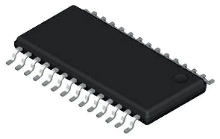
ADS1146,ADS1147,ADS1148 www.ti.com SBAS453G–JULY2009–REVISEDAUGUST2016 6 Pin Configuration and Functions PWPackage 16-PinTSSOP PWPackage TopView 28-PinTSSOP TopView DVDD 1 16 SCLK DVDD 1 28 SCLK DGND 2 27 DIN DGND 2 15 DIN CLK 3 26 DOUT/DRDY CLK 3 14 DOUT/DRDY RESET 4 25 DRDY REFP0/GPIO0 5 24 CS RESET 4 13 DRDY REFN0/GPIO1 6 23 START REFP1 7 22 AVDD REFP 5 12 CS REFN1 8 21 AVSS REFN 6 11 START VREFOUT 9 20 IEXC1 VREFCOM 10 19 IEXC2 AINP 7 10 AVDD AIN0/IEXC 11 18 AIN3/IEXC/GPIO3 AINN 8 9 AVSS AIN1/IEXC 12 17 AIN2/IEXC/GPIO2 AIN4/IEXC/GPIO4 13 16 AIN7/IEXC/GPIO7 AIN5/IEXC/GPIO5 14 15 AIN6/IEXC/GPIO6 Not to scale Not to scale PWPackage 20-PinTSSOP RHBPackage TopView 32-PinVQFN TopView Y DVDD 1 20 SCLK RD DGCNLDK 23 1198 DDIONUT/DRDY DOUT/D DRDY CS START AVDD AVSS IEXC1 IEXC2 RESET 4 17 DRDY REFP0/GPIO0 5 16 CS 32 31 30 29 28 27 26 25 DIN 1 24 AIN3/IEXC/GPIO3 REFN0/GPIO1 6 15 START SCLK 2 23 AIN2/IEXC/GPIO2 VREFOUT 7 14 AVDD NC 3 22 AIN7/IEXC/GPIO7 VREFCOM 8 13 AVSS NC 4 21 AIN6/IEXC/GPIO6 AIN0/IEXC 9 12 AIN3/IEXC/GPIO3 NC 5 Thermal Pad 20 AIN5/IEXC/GPIO5 AIN1/IEXC 10 11 AIN2/IEXC/GPIO2 NC 6 19 AIN4/IEXC/GPIO4 Not to scale DVDD 7 18 AIN1/IEXC DGND 8 17 AIN0/IEXC 9 10 11 12 13 14 15 16 CLK RESET EFP0/GPIO0 EFN0/GPIO1 REFP1 REFN1 VREFOUT VREFCOM Not to scale R R Copyright©2009–2016,TexasInstrumentsIncorporated SubmitDocumentationFeedback 5 ProductFolderLinks:ADS1146 ADS1147 ADS1148
ADS1146,ADS1147,ADS1148 SBAS453G–JULY2009–REVISEDAUGUST2016 www.ti.com PinFunctions PIN ADS1146 ADS1147 ADS1148 TYPE(1) DESCRIPTION(2) NAME TSSOP(16) TSSOP(20) TSSOP(28) VQFN(32) AIN0/IEXC — 9 11 17 I Analoginput0,optionalexcitationcurrentoutput AIN1/IEXC — 10 12 18 I Analoginput1,optionalexcitationcurrentoutput Analoginput2,optionalexcitationcurrentoutput, AIN2/IEXC/GPIO2 — 11 17 23 I/O orgeneral-purposedigitalinput/outputpin2 Analoginput3,optionalexcitationcurrentoutput, AIN3/IEXC/GPIO3 — 12 18 24 I/O orgeneral-purposedigitalinput/outputpin3 Analoginput4,optionalexcitationcurrentoutput, AIN4/IEXC/GPIO4 — — 13 19 I/O orgeneral-purposedigitalinput/outputpin4 Analoginput5,optionalexcitationcurrentoutput, AIN5/IEXC/GPIO5 — — 14 20 I/O orgeneral-purposedigitalinput/outputpin5 Analoginput6,optionalexcitationcurrentoutput, AIN6/IEXC/GPIO6 — — 15 21 I/O orgeneral-purposedigitalinput/outputpin6 Analoginput7,optionalexcitationcurrentoutput, AIN7/IEXC/GPIO7 — — 16 22 I/O orgeneral-purposedigitalinput/outputpin7 AINN 8 — — — I Negativeanaloginput AINP 7 — — — I Positiveanaloginput Positiveanalogpowersupply,connecta0.1-µFcapacitor AVDD 10 14 22 28 P toAVSS AVSS 9 13 21 27 P Negativeanalogpowersupply Externalclockinput,tietoDGNDtoactivatetheinternal CLK 3 3 3 9 I oscillator. CS 12 16 24 30 I Chipselect(activelow) DGND 2 2 2 8 G Digitalground DIN 15 19 27 1 I Serialdatainput DOUT/DRDY 14 18 26 32 O Serialdataoutput,ordataoutcombinedwithdataready DRDY 13 17 25 31 O Dataready(activelow) Digitalpowersupply,connecta0.1-µFcapacitorto DVDD 1 1 1 7 P DGND IEXC1 — — 20 26 O Excitationcurrentoutput1 IEXC2 — — 19 25 O Excitationcurrentoutput2 NC — — — 3,4,5,6 — ConnectpintoAVSSorleavefloating REFN 6 — — — I Negativeexternalreferenceinput Negativeexternalreferenceinput0, REFN0/GPIO1 — 6 6 12 I/O orgeneral-purposedigitalinput/outputpin1 REFN1 — — 8 14 I Negativeexternalreferenceinput1 REFP 5 — — — I Positiveexternalreferenceinput Positiveexternalreferenceinput0, REFP0/GPIO0 — 5 5 11 I/O orgeneral-purposedigitalinput/outputpin1 REFP1 — — 7 13 I Positiveexternalreferenceinput1 RESET 4 4 4 10 I Reset(activelow) SCLK 16 20 28 2 I Serialclockinput START 11 15 23 29 I Conversionstart ThermalPad — — — 33 — ConnectpintoAVSSorleavefloating Negativeinternalreferencevoltageoutput,connectto VREFCOM — 8 10 16 O AVSSwhenusingaunipolarsupplyortothemid-voltage groundwhenusingabipolarsupply Positiveinternalreferencevoltageoutput,connecta VREFOUT — 7 9 15 O capacitorintherangeof1µFto47µFtoVREFCOM (1) G=Ground,I=Input,O=Output,P=Power (2) SeeUnusedInputsandOutputsforunusedpinconnections. 6 SubmitDocumentationFeedback Copyright©2009–2016,TexasInstrumentsIncorporated ProductFolderLinks:ADS1146 ADS1147 ADS1148
ADS1146,ADS1147,ADS1148 www.ti.com SBAS453G–JULY2009–REVISEDAUGUST2016 7 Specifications 7.1 Absolute Maximum Ratings See(1) MIN MAX UNIT AVDDtoAVSS –0.3 5.5 Power-supplyvoltage AVSStoDGND –2.8 0.3 V DVDDtoDGND –0.3 5.5 Analoginputvoltage AINx,REFPx,REFNx,VREFOUT,VREFCOM,IEXC1,IEXC2 AVSS–0.3 AVDD+0.3 V Digitalinputvoltage SCLK,DIN,DOUT/DRDY,DRDY,CS,START,RESET,CLK DGND–0.3 DVDD+0.3 V Continuous,anypinexceptpowersupplypins –10 10 Inputcurrent mA Momentary,anypinexceptpowersupplypins –100 100 Junction,TJ 150 Temperature °C Storage,Tstg –60 150 (1) StressesbeyondthoselistedunderAbsoluteMaximumRatingsmaycausepermanentdamagetothedevice.Thesearestressratings only,whichdonotimplyfunctionaloperationofthedeviceattheseoranyotherconditionsbeyondthoseindicatedunderRecommended OperatingConditions.Exposuretoabsolute-maximum-ratedconditionsforextendedperiodsmayaffectdevicereliability. 7.2 ESD Ratings VALUE UNIT Human-bodymodel(HBM),perANSI/ESDA/JEDECJS-001(1) ±2000 V(ESD) Electrostaticdischarge Charged-devicemodel(CDM),perJEDECspecificationJESD22-C101(2) ±750 V (1) JEDECdocumentJEP155statesthat500-VHBMallowssafemanufacturingwithastandardESDcontrolprocess. (2) JEDECdocumentJEP157statesthat250-VCDMallowssafemanufacturingwithastandardESDcontrolprocess. Copyright©2009–2016,TexasInstrumentsIncorporated SubmitDocumentationFeedback 7 ProductFolderLinks:ADS1146 ADS1147 ADS1148
ADS1146,ADS1147,ADS1148 SBAS453G–JULY2009–REVISEDAUGUST2016 www.ti.com 7.3 Recommended Operating Conditions Overoperatingambienttemperaturerange(unlessotherwisenoted) MIN NOM MAX UNIT POWERSUPPLY AVDDtoAVSS 2.7 5.25 Analogpowersupply AVSStoDGND –2.65 0.1 V AVDDtoDGND 2.25 5.25 Digitalpowersupply DVDDtoDGND 2.7 5.25 V ANALOGINPUTS(1) VIN Differentialinputvoltage V(AINP)–V(AINN)(2) –VREF/Gain VREF/Gain V VCM Common-modeinputvoltage (V(AINP)+V(AINN))/2 SeeEquation3 VOLTAGEREFERENCEINPUTS(3) VREF Differentialreferenceinputvoltage V(REFPx)–V(REFNx) 0.5 (AVDD–AVSS)–1 V V(REFNx) Absolutenegativereferencevoltage AVSS–0.1 V(REFPx)–0.5 V V(REFPx) Absolutepositivereferencevoltage V(REFNx)+0.5 AVDD+0.1 V EXTERNALCLOCKINPUT(4) fCLK Externalclockfrequency 1 4.5 MHz Externalclockdutycycle 25% 75% GENERAL-PURPOSEINPUTSANDOUTPUTS(GPIO) GPIOinputvoltage AVSS AVDD V DIGITALINPUTS Digitalinputvoltage DGND DVDD V TEMPERATURERANGE TA Operatingambienttemperature –40 125 °C Specifiedambienttemperature –40 105 °C (1) AIN andAIN denotethepositiveandnegativeinputsofthePGA. P N (2) ForV >2.7V,thedifferentialinputvoltagemustnotexceed2.7V/Gain. REF (3) REFPxandREFNxdenotethedifferentialreferenceinputpair(ADS1146,ADS1147),oroneofthetwoavailabledifferentialreference inputpairs(ADS1148). (4) Externalclockonlyrequirediftheinternaloscillatorisnotused. 7.4 Thermal Information ADS1146 ADS1147 ADS1148 THERMALMETRIC(1) PW(TSSOP) PW(TSSOP) PW(TSSOP) RHB(VQFN) UNIT 16PINS 20PINS 28PINS 32PINS R Junction-to-ambientthermalresistance 95.2 87.4 74.2 32.5 °C/W θJA R Junction-to-case(top)thermalresistance 28.9 21.7 20.2 23.9 °C/W θJC(top) R Junction-to-boardthermalresistance 41 39.6 31.8 6.6 °C/W θJB ψ Junction-to-topcharacterizationparameter 1.5 0.8 0.8 0.3 °C/W JT ψ Junction-to-boardcharacterizationparameter 40.4 38.9 31.3 6.6 °C/W JB R Junction-to-case(bottom)thermalresistance — — — 1.6 °C/W θJC(bot) (1) Formoreinformationabouttraditionalandnewthermalmetrics,seetheSemiconductorandICPackageThermalMetricsapplication report. 8 SubmitDocumentationFeedback Copyright©2009–2016,TexasInstrumentsIncorporated ProductFolderLinks:ADS1146 ADS1147 ADS1148
ADS1146,ADS1147,ADS1148 www.ti.com SBAS453G–JULY2009–REVISEDAUGUST2016 7.5 Electrical Characteristics MinimumandmaximumspecificationsapplyfromT =–40°Cto+105°C.TypicalspecificationsareatT =25°C. A A AllspecificationsareatAVDD=5V,DVDD=3.3V,AVSS=0V,V =2.048V,andf =4.096MHz(unlessotherwise REF CLK noted). PARAMETER TESTCONDITIONS MIN TYP MAX UNIT ANALOGINPUTS Differentialinputcurrent 100 pA Absoluteinputcurrent SeeTable4 PGA PGAgainsettings 1,2,4,8,16,32,64,128 V/V SYSTEMPERFORMANCE Resolution Nomissingcodes 16 Bits DR Datarate 5,10,20,40,80,160,320,640,1000,2000 SPS ADCconversiontime Single-cyclesettling SeeTable10 Differentialinput,endpointfit, INL Integralnonlinearity –1 0.5 1 LSB Gain=1,VCM=2.5V Offseterror Aftercalibration –1 1 LSB Gain=1 100 nV/°C Offsetdrift Gain=128 15 nV/°C Gainerror ExcludingVREFerrors –0.5% 0.5% Gain=1,excludesVREFdrift 1 ppm°C Gaindrift Gain=128,excludesVREFdrift –3.5 ppm/°C Noise SeeTable1andTable2 NMRR Normalmoderejection SeeTable6 AtDC,Gain=1 90 CMRR Common-moderejection dB AtDC,Gain=32 100 PSRR Powersupplyrejection AVDD,DVDDatDC 100 dB VOLTAGEREFERENCEINPUTS Referenceinputcurrent 30 nA INTERNALVOLTAGEREFERENCE VREF Internalreferencevoltage 2.038 2.048 2.058 V Referencedrift(1) TA=–40°Cto+105°C 20 50 ppm/°C Outputcurrent(2) –10 10 mA Loadregulation 50 µV/mA Start-uptime SeeTable7 INTERNALOSCILLATOR Internaloscillatorfrequency 3.89 4.096 4.3 MHz EXCITATIONCURRENTSOURCES(IDACs) Outputcurrentsettings 50,100,250,500,750,1000,1500 µA Compliancevoltage Allcurrents SeeFigure9andFigure10 Absoluteerror Allcurrents,eachIDAC –6% ±1% 6% Absolutemismatch Allcurrents,betweenIDACs ±0.2% Temperaturedrift EachIDAC 200 ppm/°C Temperaturedriftmatching BetweenIDACs 10 ppm/°C BURN-OUTCURRENTSOURCES Burn-outcurrentsourcesettings 0.5,2,10 µA (1) Specifiedbythecombinationofdesignandfinalproductiontest. (2) Donotexceedthisloadingontheinternalvoltagereference. Copyright©2009–2016,TexasInstrumentsIncorporated SubmitDocumentationFeedback 9 ProductFolderLinks:ADS1146 ADS1147 ADS1148
ADS1146,ADS1147,ADS1148 SBAS453G–JULY2009–REVISEDAUGUST2016 www.ti.com Electrical Characteristics (continued) MinimumandmaximumspecificationsapplyfromT =–40°Cto+105°C.TypicalspecificationsareatT =25°C. A A AllspecificationsareatAVDD=5V,DVDD=3.3V,AVSS=0V,V =2.048V,andf =4.096MHz(unlessotherwise REF CLK noted). PARAMETER TESTCONDITIONS MIN TYP MAX UNIT BIASVOLTAGE Biasvoltage (AVDD+AVSS)/2 V Biasvoltageoutputimpedance 400 Ω TEMPERATURESENSOR Outputvoltage TA=25°C 118 mV Temperaturecoefficient 405 µV/°C GENERAL-PURPOSEINPUTSANDOUTPUTS(GPIO) VIL Low-levelinputvoltage AVSS 0.3×AVDD V VIH High-levelinputvoltage 0.7×AVDD AVDD V VOL Low-leveloutputvoltage IOL=1mA AVSS 0.2×AVDD V VOH High-leveloutputvoltage IOH=1mA 0.8×AVDD V DIGITALINPUTSANDOUTPUTS(OTHERTHANGPIO) VIL Low-levelinputvoltage DGND 0.3×DVDD V VIH High-levelinputvoltage 0.7×DVDD DVDD V VOL Low-leveloutputvoltage IOL=1mA DGND 0.2×DVDD V VOH High-leveloutputvoltage IOH=1mA 0.8×DVDD V Inputleakage DGND<VIN<DVDD –10 10 µA POWERSUPPLY Power-downmode 0.1 Converting,AVDD=3.3V, 212 DR=20SPS,externalreference IAVDD Analogsupplycurrent Converting,AVDD=5V, µA 225 DR=20SPS,externalreference Additionalcurrentwithinternalreference 180 enabled Power-downmode 0.2 Normaloperation,DVDD=3.3V, 210 IDVDD Digitalsupplycurrent DR=20SPS,internaloscillator µA Normaloperation,DVDD=5V, 230 DR=20SPS,internaloscillator AVDD=DVDD=3.3V, DR=20SPS,internaloscillator,external 1.4 reference PD Powerdissipation mW AVDD=DVDD=5V, DR=20SPS,internaloscillator,external 2.3 reference 10 SubmitDocumentationFeedback Copyright©2009–2016,TexasInstrumentsIncorporated ProductFolderLinks:ADS1146 ADS1147 ADS1148
ADS1146,ADS1147,ADS1148 www.ti.com SBAS453G–JULY2009–REVISEDAUGUST2016 7.6 Timing Requirements AtT =–40°Cto+105°CandDVDD=2.7Vto5.5V(unlessotherwisenoted) A PARAMETER MIN NOM MAX UNIT SERIALINTERFACE(SEEFigure1ANDFigure2) t Delaytime,firstSCLKrisingedgeafterCSfallingedge 10 ns CSSC t Delaytime,CSrisingedgeafterfinalSCLKfallingedge 7 t (1) SCCS CLK t Pulseduration,CShigh 5 t CSPW CLK 488 ns t SCLKperiod SCLK 64 Conversions t Pulseduration,SCLKhigh 0.25 0.75 t SPWH SCLK t Pulseduration,SCLKlow 0.25 0.75 t SPWL SCLK t Setuptime,DINvalidbeforeSCLKfallingedge 5 ns DIST t Holdtime,DINvalidafterSCLKfallingedge 5 ns DIHD t Setuptime,SCLKlowbeforeDRDYrisingedge 5 t STD CLK t Delaytime,SCLKrisingedgeafterDRDYfallingedge 1 t DTS CLK MINIMUMSTARTTIMEPULSEDURATION(SEEFigure3) t Pulseduration,STARThigh 3 t START CLK RESETPULSEDURATION,SERIALINTERFACECOMMUNICATIONAFTERRESET(SEEFigure4) t Pulseduration,RESETlow 4 t RESET CLK t Delaytime,SCLKrisingedge(startofserialinterfacecommunication) 0.6(2) ms RHSC afterRESETrisingedge (1) t =1/f .Thedefaultclockfrequencyf =4.096MHz. CLK CLK CLK (2) Applicableonlywhenf =4.096MHz,scalesproportionallywithf frequency. CLK CLK 7.7 Switching Characteristics AtT =–40°Cto+105°CandDVDD=2.7Vto5.5V(unlessotherwisenoted;seeFigure1andFigure2) A PARAMETER TESTCONDITIONS MIN TYP MAX UNIT Propagationdelaytime, DVDD≤3.6V 50 t ns DOPD SCLKrisingedgetovalidnewDOUT DVDD>3.6V 180 t DOUTholdtime 0 ns DOHD Propagationdelaytime, t 10 ns CSDO CSrisingedgetoDOUThighimpedance t Pulseduration,DRDYhigh 3 t PWH CLK Copyright©2009–2016,TexasInstrumentsIncorporated SubmitDocumentationFeedback 11 ProductFolderLinks:ADS1146 ADS1147 ADS1148
ADS1146,ADS1147,ADS1148 SBAS453G–JULY2009–REVISEDAUGUST2016 www.ti.com CS tCSPW tCSSC tSCLK tSPWH tSCCS SCLK tDIST tDIHD tSPWL DIN DIN[0] DIN[7] DIN[6] DIN[5] DIN[4] DIN[1] DIN[0] tDOPD tDOHD DOUT/DRDY DOUT[7] DOUT[6] DOUT[5] DOUT[4] DOUT[1] DOUT[0] tCSDO Figure1. SerialInterfaceTiming,DRDYMODEBit=0 tDTS tPWH DRDY tSTD(1) 1 2 3 4 5 6 7 8 SCLK(2) (1) ThistimingdiagramisapplicableonlywhentheCSpinislow.SCLKdoesnotneedtobelowduringt whenCSis STD high. (2) SCLKmustonlybesentinmultiplesofeightduringpartialretrievalofoutputdata. Figure2. SerialInterfaceTimingtoAllowConversionResultLoading START tSTART Figure3. MinimumStartPulseDuration t RESET RESET CS SCLK t RHSC Figure4. ResetPulseDurationandSerialInterfaceCommunicationAfterReset 12 SubmitDocumentationFeedback Copyright©2009–2016,TexasInstrumentsIncorporated ProductFolderLinks:ADS1146 ADS1147 ADS1148
ADS1146,ADS1147,ADS1148 www.ti.com SBAS453G–JULY2009–REVISEDAUGUST2016 7.8 Typical Characteristics T =25°C,AVDD=5V,AVSS=0V,andV =2.5V(unlessotherwisenoted) A REF 0 3.0 32 Units 2.5 −20 2.0 nce Drift (ppm) −−6400 Rate Error (%) -1100....50505 DDVDVDDD = =3 .53VV Refere −80 Data --11..05 −100 -2.0 -2.5 −120 -3.0 0 200 400 600 800 1000 -40 -20 0 20 40 60 80 100 120 Time (hours) Temperature (°C) G000 Figure5.InternalReferenceLong-TermDrift Figure6.DataRateErrorvsTemperature 1.002 0.004 1.5mA Setting, 10 Units 1.001 0.003 nt 1.000 d Output Curre 0000....999999999876 50mA 500mA 120500mmAA -mIEXC2 (A) 00..0000210 alize 0.995 750mA XC1 -0.001 orm 0.994 IDAC Current Settings IE -0.002 N 0.993 1mA -0.003 0.992 1.5mA 0.991 -0.004 2.0 2.5 3.0 3.5 4.0 4.5 5.0 5.5 6.0 -40 -20 0 20 40 60 80 100 120 AVDD (V) Temperature (°C) Figure7.IDACLineRegulation Figure8.IDACDrift 1.1 1.01 1 0.9 1.005 nt nt e 0.8 e urr urr 1 C 0.7 C C C A 0.6 A D D0.995 ed I 0.5 50µA ed I maliz 0.4 120500µµAA maliz 0.99 or 0.3 500µA or N N 0.2 750µA 0.985 1mA 0.1 1.5mA 0 0.98 0 1 2 3 4 5 0 1 2 3 4 5 Voltage (V) Voltage (V) Figure9.IDACVoltageCompliance Figure10.IDACVoltageCompliance Copyright©2009–2016,TexasInstrumentsIncorporated SubmitDocumentationFeedback 13 ProductFolderLinks:ADS1146 ADS1147 ADS1148
ADS1146,ADS1147,ADS1148 SBAS453G–JULY2009–REVISEDAUGUST2016 www.ti.com Typical Characteristics (continued) T =25°C,AVDD=5V,AVSS=0V,andV =2.5V(unlessotherwisenoted) A REF 600 290 550 270 500 A) 450 A) mCurrent ( 430500 AVDD = 5VAVDD = 3.3V mCurrent ( 225300 DVDD = 5V Analog 320500 Digital 210 DVDD = 3.3V 200 190 150 100 170 5 10 20 40 80 160 320 640 1000 2000 5 10 20 40 80 160 320 640 10002000 Data Rate (SPS) Data Rate (SPS) Figure11.AnalogSupplyCurrentvsDataRate Figure12.DigitalSupplyCurrentvsDataRate 800 330 AVDD = 5V 2kSPS DVDD = 5V 700 310 2kSPS 600 A) 320/640/1kSPS A) 290 mAnalog Current ( 543200000000 405//8100//12600SSPPSS mDigital Current ( 222753000 320/640/1kSPS 40/80/160SPS 100 210 5/10/20SPS 0 190 -40 -20 0 20 40 60 80 100 120 -40 -20 0 20 40 60 80 100 120 Temperature (°C) Temperature (°C) Figure13.AnalogSupplyCurrentvsTemperature Figure14.DigitalSupplyCurrentvsTemperature 700 310 AVDD = 3.3V DVDD = 3.3V 2kSPS 600 290 2kSPS A) 500 A) malog Current ( 430000 5/10/20SPS 34200/8/604/106/10kSSPPSS mgital Current ( 222753000 320/640/1kSPS An 200 Di 40/80/160SPS 100 210 5/10/20SPS 0 190 -40 -20 0 20 40 60 80 100 120 -40 -20 0 20 40 60 80 100 120 Temperature (°C) Temperature (°C) Figure15.AnalogSupplyCurrentvsTemperature Figure16.DigitalSupplyCurrentvsTemperature 14 SubmitDocumentationFeedback Copyright©2009–2016,TexasInstrumentsIncorporated ProductFolderLinks:ADS1146 ADS1147 ADS1148
ADS1146,ADS1147,ADS1148 www.ti.com SBAS453G–JULY2009–REVISEDAUGUST2016 8 Parameter Measurement Information 8.1 Noise Performance TheADCnoiseperformanceisoptimizedbyadjustingthedatarateandPGAsetting.Generally,thelowestinput- referred noise is achieved using the highest gain possible, consistent with the input signal range. Do not set the gain too high or the result is ADC overrange. Noise also depends on the output data rate. As the data rate reduces, the ADC bandwidth correspondingly reduces. This reduction in total bandwidth results in lower overall noise. Table 1 and Table 2 summarize the noise performance of the device. The data are representative of typical noise performance at T = 25°C. The data shown are the result of averaging the readings from multiple A devicesandweremeasuredwiththeinputsshortedtogether. Table 1 lists the input-referred noise in units of µV for the conditions shown. Table 2 lists the corresponding PP datainunitsofENOB(effectivenumberofbits)whereENOBforthepeak-to-peaknoiseisdefinedinEquation1. ENOB=ln((2×V /Gain)/V )/ln(2) REF NPP where • V istheinputreferredpeak-to-peaknoisevoltage (1) NPP Table1.NoiseinµV PP AtV =2.048V,AVDD=5V,AVSS=0V REF DATARATE PGASETTING (SPS) 1 2 4 8 16 32 64 128 5 62.5(1) 31.25(1) 15.63(1) 7.81(1) 3.91(1) 1.95(1) 0.98(1) 0.49(1) 10 62.5(1) 31.25(1) 15.63(1) 7.81(1) 3.91(1) 1.95(1) 0.98(1) 0.49(1) 20 62.5(1) 31.25(1) 15.63(1) 7.81(1) 3.91(1) 1.95(1) 0.98(1) 0.55 40 62.5(1) 31.25(1) 15.63(1) 7.81(1) 3.91(1) 1.95(1) 0.98(1) 0.75 80 62.5(1) 31.25(1) 15.63(1) 7.81(1) 3.91(1) 1.95(1) 1.09 0.98 160 62.5(1) 31.25(1) 15.63(1) 7.81(1) 3.91(1) 1.95(1) 1.88 1.57 320 62.5(1) 35.3 17.52 8.86 4.35 3.03 2.44 2.34 640 93.06 45.2 18.73 12.97 6.51 4.2 3.69 3.5 1000 284.59 129.77 61.3 33.04 16.82 9.08 5.42 4.65 2000 273.39 130.68 67.13 36.16 19.22 9.87 6.93 6.48 (1) Peak-to-peaknoiseroundedupto1LSB. Table2.EffectiveNumberofBitsFromPeak-to-PeakNoise AtV =2.048V,AVDD=5V,AVSS=0V REF DATARATE PGASETTING (SPS) 1 2 4 8 16 32 64 128 5 16 16 16 16 16 16 16 16 10 16 16 16 16 16 16 16 16 20 16 16 16 16 16 16 16 15.8 40 16 16 16 16 16 16 16 15.4 80 16 16 16 16 16 16 15.8 15 160 16 16 16 16 16 16 15.1 14.3 320 16 15.8 15.8 15.8 15.8 15.4 14.7 13.7 640 15.4 15.5 15.7 15.3 15.3 14.9 14.1 13.2 1000 13.8 13.9 14 13.9 13.9 13.8 13.5 12.7 2000 13.9 13.9 13.9 13.8 13.7 13.7 13.2 12.3 Copyright©2009–2016,TexasInstrumentsIncorporated SubmitDocumentationFeedback 15 ProductFolderLinks:ADS1146 ADS1147 ADS1148
ADS1146,ADS1147,ADS1148 SBAS453G–JULY2009–REVISEDAUGUST2016 www.ti.com 9 Detailed Description 9.1 Overview TheADS1146,ADS1147andADS1148devicesarehighlyintegrated16-bitdataconverters.Thedevicesinclude a low-noise, high-input impedance programmable gain amplifier (PGA), a delta-sigma (ΔΣ) ADC with an adjustablesingle-cyclesettlingdigitalfilter,internaloscillator,andanSPI-compatibleserialinterface. The ADS1147 and ADS1148 also include a flexible input multiplexer with system monitoring capability and general-purpose I/O settings, a low-drift voltage reference, and two matched current sources for sensor excitation.Figure17andFigure18showthevariousfunctionsincorporatedintoeachdevice. 9.2 Functional Block Diagrams AVDD REFP REFN DVDD Burnout Detect ADS1146 VBIAS SCLK DIN Serial DRDY AAIINNNP IMnpuuxt PGA M3rodd ßOu(cid:8)lra(cid:3)d(cid:3)teorr AdDjFuiigsltitetaarblle InCtAoenrnftadrocel DCOSUT/DRDY START RESET Internal Oscillator Burnout Detect AVSS CLK DGND Copyright ' 2016, Texas Instruments Incorporated Figure17. ADS1146Diagram REFP0/REFN0/ ADS1148 Only AVDD GPIO0 GPIO1 REFP1 REFN1 VREFOUT VREFCOM DVDD Burnout Detect VREF Mux Voltage ADS1147 Reference ADS1148 VBIAS GPIO AIN0/IEXC System SCLK AIN1/IEXC Monitor DIN Serial AIN2/IEXC/GPIO2 DRDY 3rd Order Adjustable Interface AIN3/IEXC/GPIO3 IMnpuuxt PGA ß(cid:8)(cid:3)(cid:3) Digital And DOUT/DRDY AIN4/IEXC/GPIO4 Modulator Filter Control CS AIN5/IEXC/GPIO5 START AIN6/IEXC/GPIO6 Dual RESET IDACs AIN7/IEXC/GPIO7 Internal Oscillator ADS1148 Only Burnout Detect AVSS IEXC1 IEXC2 CLK DGND ADS1148 Only Copyright ' 2016, Texas Instruments Incorporated Figure18. ADS1147andADS1148Diagram 16 SubmitDocumentationFeedback Copyright©2009–2016,TexasInstrumentsIncorporated ProductFolderLinks:ADS1146 ADS1147 ADS1148
ADS1146,ADS1147,ADS1148 www.ti.com SBAS453G–JULY2009–REVISEDAUGUST2016 9.3 Feature Description 9.3.1 ADCInputandMultiplexer The ADC measures the input signal through the onboard PGA. All analog inputs are connected to the internal AIN or AIN analog inputs through the analog multiplexer. Figure 19 shows a block diagram of the analog input P N multiplexer. Theinputmultiplexerconnectstoeight(ADS1148)orfour(ADS1147)analoginputs.Anyanaloginputpincanbe selected as the positive input or negative input through the MUX0 register, while the ADS1146 has AINP and AINN connections for a single differential channel. The multiplexer also allows the on-chip excitation current and biasvoltagetobeselectedtoaspecificchannel. Through the input multiplexer, the ambient temperature (internal temperature sensor), AVDD, DVDD, and externalreferencecanallbeselectedformeasurement.SeetheSystemMonitorsectionformoredetails. OntheADS1147andADS1148,theanaloginputscanalsobeconfiguredasgeneral-purposeinputsandoutputs (GPIOs).SeetheGeneral-PurposeDigitalI/O sectionformoredetails. AVDD AVDD IDAC2 IDAC1 System Monitors AVSS AVDD VBIAS AVDD AVDD AIN0 AVSS AVDD VBIAS Temperature VREFP Diode AIN1 VREFN ADS1147/8 OnlyAVSS AVDD VBIAS VREFP1/4 VREFN1/4 AIN2 VREFP0/4 VREFN0/4 AVSS AVDD VBIAS AVDD/4 AIN3 AVSS/4 DVDD/4 ADS1148 Only DGND/4 AVSS AVDD VBIAS AIN4 AVDD AVSS AVDD VBIAS Burnout Current Source (0.5 µA, 2 µA, 10 µA) AIN5 AINP To PGA AVSS AVDD VBIAS AINN ADC AIN6 Burnout Current Source AVSS AVDD VBIAS (0.5 µA, 2 µA, 10 µA) AIN7 AVSS Copyright ' 2016, Texas Instruments Incorporated Figure19. AnalogInputMultiplexerCircuit Copyright©2009–2016,TexasInstrumentsIncorporated SubmitDocumentationFeedback 17 ProductFolderLinks:ADS1146 ADS1147 ADS1148
ADS1146,ADS1147,ADS1148 SBAS453G–JULY2009–REVISEDAUGUST2016 www.ti.com Feature Description (continued) ESD diodes protect the ADC inputs. To prevent these diodes from turning on, make sure the voltages on the input pins do not go below AVSS by more than 100 mV, and do not exceed AVDD by more than 100 mV, as showninEquation2.NotethatthesamecautionistrueiftheinputsareconfiguredtobeGPIOs. AVSS–100mV<V <AVDD+100mV (2) (AINX) 9.3.2 Low-NoisePGA The ADS1146, ADS1147, and ADS1148 feature a low-drift, low-noise, high input impedance programmable gain amplifier (PGA). The PGA can be set to gains of 1, 2, 4, 8, 16, 32, 64, or 128 by register SYS0. Figure 20 shows asimplifieddiagramofthePGA. The PGA consists of two chopper-stabilized amplifiers (A1 and A2) and a resistor feedback network that sets the gain of the PGA. The PGA input is equipped with an electromagnetic interference (EMI) filter, as shown in Figure 20. As with any PGA, ensure that the input voltage stays within the specified common-mode input range. Thecommon-modeinput(V )mustbewithintherangeshowninEquation3. CM § V (cid:152)Gain• § V (cid:152)Gain• ¤¤'AVSS (cid:14) 0.1 V (cid:14) IN (MAX2) ‚‚„dVCMd¤¤'AVDD (cid:16) 0.1 V (cid:16) IN (MA2X) ‚‚„ (3) 454 (cid:13) AINP + A1 7.5 pF RF R 7.5 pF RG C ADC R RF 7.5 pF 454 (cid:13) A2 AINN + 7.5 pF Figure20. SimplifiedDiagramofthePGA Gain is changed inside the device using a variable resistor, R . The differential full-scale input voltage range G (FSR)ofthePGAisdefinedbythegainsettingandthereferencevoltageused,asshowninEquation4. FSR=±V /Gain (4) REF Table3showsthecorrespondingfull-scaleinputrangeswhenusingtheinternal2.048-Vreference. Table3.PGAFull-ScaleRange PGAGAINSETTING FSR 1 ±2.048V 2 ±1.024V 4 ±0.512V 8 ±0.256V 16 ±0.128V 32 ±0.064V 64 ±0.032V 128 ±0.016V 18 SubmitDocumentationFeedback Copyright©2009–2016,TexasInstrumentsIncorporated ProductFolderLinks:ADS1146 ADS1147 ADS1148
ADS1146,ADS1147,ADS1148 www.ti.com SBAS453G–JULY2009–REVISEDAUGUST2016 9.3.2.1 PGACommon-ModeVoltageRequirements To stay within the linear operating range of the PGA, the input signals must meet certain requirements that are discussedinthissection. The outputs of both amplifiers (A1 and A2) in Figure 20 can not swing closer to the supplies (AVSS and AVDD) than 100 mV. If the outputs OUT and OUT are driven to within 100 mV of the supply rails, the amplifiers P N saturate and consequently become nonlinear. To prevent this nonlinear operating condition, the output voltages mustmeetEquation5. AVSS+0.1V≤V ,V ≤AVDD–0.1V (5) (OUTN) (OUTP) Translating the requirements of Equation 5 into requirements referred to the PGA inputs (AIN and AIN ) is P N beneficial because there is no direct access to the outputs of the PGA. The PGA employs a symmetrical design; therefore, the common-mode voltage at the output of the PGA can be assumed to be the same as the common- modevoltageoftheinputsignal,asshowninFigure21. AINP + A1 - ½ VIN RF OUTP ½ Gain·V IN V = ½ (V + V ) R CM (AINP) (AINN) G ½ Gain·V IN R F ½ VIN OUTN - A2 AINN + Figure21. PGACommon-ModeVoltage Thecommon-modevoltageiscalculatedusingEquation6. V =½(V +V )=½(V +V ) (6) CM (AINP) (AINN) (OUTP) (OUTN) ThevoltagesatthePGAinputs(AIN andAIN )canbeexpressedasEquation7andEquation8. P N V =V +½V (7) (AINP) CM IN V =V –½V (8) (AINN) CM IN Theoutputvoltages(V andV )canthenbecalculatedasEquation9andEquation10. (OUTP) (OUTN) V =V +½Gain×V (9) (OUTP) CM IN V =V –½Gain×V (10) (OUTN) CM IN The requirements for the output voltages of amplifiers A1 and A2 (Equation 5) can now be translated into requirements for the input common-mode voltage range using Equation 9 and Equation 10, which are given in Equation11andEquation12. V ≥AVSS+0.1V+½Gain×V (11) CM(MIN) IN(MAX) V ≤AVDD–0.1V–½Gain×V (12) CM(MAX) IN(MAX) To calculate the minimum and maximum common-mode voltage limits, the maximum differential input voltage (V ) that occurs in the application must be used. V can be less than the maximum possible full-scale IN (MAX) IN (MAX) value. Copyright©2009–2016,TexasInstrumentsIncorporated SubmitDocumentationFeedback 19 ProductFolderLinks:ADS1146 ADS1147 ADS1148
ADS1146,ADS1147,ADS1148 SBAS453G–JULY2009–REVISEDAUGUST2016 www.ti.com 9.3.2.2 PGACommon-ModeVoltageCalculationExample The following paragraphs explain how to apply Equation 11 and Equation 12 to a hypothetical application. The setup for this example is AVDD = 3.3 V, AVSS = 0 V, and gain = 16, using an external reference, V = 2.5 V. REF The maximum possible differential input voltage V = (V – V ) that can be applied is then limited to the IN (AINP) (AINN) full-scale range of FSR = ±2.5 V / 16 = ±0.156 V. Consequently, Equation 11 and Equation 12 yield an allowed V rangeof1.35V≤ V ≤ 1.95V. CM CM If the sensor signal connected to the inputs in this hypothetical application does not make use of the entire full- scale range but is limited to V = ±0.1 V, for example, then this reduced input signal amplitude relaxes the IN (MAX) V restrictionto0.9V≤ V ≤ 2.4V. CM CM In the case of a fully-differential sensor signal, each input (AIN , AIN ) can swing up to ±50 mV around the P N common-mode voltage (V + V ) / 2, which must remain between the limits of 0.9 V and 2.4 V. The (AINP) (AINN) output of a symmetrical wheatstone bridge is an example of a fully-differential signal. Figure 22 shows a situation where the common-mode voltage of the input signal is at the lowest limit. V is exactly at 0.1 V in this case. (OUTN) Any further decrease in common-mode voltage (V ) or increase in differential input voltage (V ) drives V CM IN (OUTN) below0.1VandsaturatesamplifierA2. V(AINP) = 0.95 V + A1 - 50 mV R V = 1.7 V F (OUTP) 800 mV VCM = 0.9 V RF / 7.5 800 mV R F 50 mV V(OUTN) = 0.1 V - A2 V(AINN) = 0.85 V + Figure22. ExampleWhereV isattheLowestLimit CM In contrast, the signal of an RTD is of a pseudo-differential nature (if implemented as shown in the 3-Wire RTD MeasurementSystemsection),wherethenegativeinputisheldataconstantvoltageotherthan0Vandonlythe voltageonthepositiveinputchanges.Whenapseudo-differentialsignalmustbemeasured,thenegativeinputin this example must be biased at a voltage from 0.85 V to 2.35 V. The positive input can then swing up to V IN (MAX) = 100 mV above the negative input. In this case, the common-mode voltage changes at the same time the voltage on the positive input changes. That is, while the input signal swings between 0 V ≤ V ≤ V , the IN IN (MAX) common-mode voltage swings between V ≤ V ≤ V + ½ V . Satisfying the common-mode (AINN) CM (AINN) IN (MAX) voltage requirements for the maximum input voltage V ensures the requirements are met throughout the IN (MAX) entiresignalrange. 20 SubmitDocumentationFeedback Copyright©2009–2016,TexasInstrumentsIncorporated ProductFolderLinks:ADS1146 ADS1147 ADS1148
ADS1146,ADS1147,ADS1148 www.ti.com SBAS453G–JULY2009–REVISEDAUGUST2016 Figure23andFigure24showexamplesofbothfully-differentialandpseudo-differentialsignals,respectively. AIN P AIN V P CM 100 mV V 1.0 V CM 100 mV 1.0 V AIN N AIN N 0 V 0 V Figure23.Fully-DifferentialInputSignal Figure24.Pseudo-DifferentialInputSignal NOTE With a unipolar power supply, the input range does not extend to the ground. Equation 11 andEquation12showthecommon-modevoltagerequirements. • V ≥AVSS+0.1V+ ½Gain×V CM(MIN) IN(MAX) • V ≤AVDD–0.1V–½Gain×V CM(MAX) IN(MAX) 9.3.2.3 AnalogInputImpedance Thedeviceinputsarebufferedthroughahigh-inputimpedancePGAbeforetheyreachthe ΔΣmodulator.Forthe majority of applications, the input current is minimal and can be neglected. However, because the PGA is chopper-stabilized for noise and offset performance, the input impedance is best described as a small absolute input current. The absolute input current for selected channels is approximately proportional to the selected modulator clock. Table 4 shows the typical values for these currents with a differential voltage coefficient and the correspondinginputimpedancesoverdatarate. Table4.TypicalValuesforAnalogInputCurrentOverDataRate(1) CONDITION ABSOLUTEINPUTCURRENT EFFECTIVEINPUTIMPEDANCE DR=5SPS,10SPS,20SPS ±(0.5nA+0.1nA/V) 5000MΩ DR=40SPS,80SPS,160SPS ±(2nA+0.5nA/V) 1200MΩ DR=320SPS,640SPS,1kSPS ±(4nA+1nA/V) 600MΩ DR=2kSPS ±(8nA+2nA/V) 300MΩ (1) InputcurrentwithV =2.5V,T =25°C,AVDD=5V,andAVSS=0V. CM A 9.3.3 ClockSource The device can use either the internal oscillator or an external clock. Connect the CLK pin to DGND before power-on or reset to activate the internal oscillator. Connecting an external clock to the CLK pin at any time deactivates the internal oscillator, with the device then operating on the external clock. After the device switches to the external clock, it cannot be switched back to the internal oscillator without cycling the power supplies or resettingthedevice. Copyright©2009–2016,TexasInstrumentsIncorporated SubmitDocumentationFeedback 21 ProductFolderLinks:ADS1146 ADS1147 ADS1148
ADS1146,ADS1147,ADS1148 SBAS453G–JULY2009–REVISEDAUGUST2016 www.ti.com 9.3.4 Modulator A third-order delta-sigma modulator is used in the ADS1146, ADS1147, and ADS1148 devices. The modulator convertstheanaloginputvoltageintoapulsecodemodulated(PCM)datastream.Tosavepower,themodulator clockrunsfrom32kHzupto512kHzfordifferentdatarates,asshowninTable5. Table5.ModulatorClockFrequencyforDifferentDataRates DATARATE MODULATORRATE(f )(1) MOD f /f (SPS) (kHz) CLK MOD 5,10,20 32 128 40,80,160 128 32 320,640,1000 256 16 2000 512 8 (1) Usingtheinternaloscillatororanexternal4.096-MHzclock. 9.3.5 DigitalFilter The ADC uses linear-phase finite impulse response (FIR) digital filters that can be adjusted for different output datarates.Thedigitalfilteralwayssettlesinasinglecycle. Table 6 shows the exact data rates when an external clock equal to 4.096 MHz is used. Also shown is the signal –3-dB bandwidth, and the 50-Hz and 60-Hz attenuation. For good 50-Hz or 60-Hz rejection, use a data rate of 20SPSorslower. The frequency responses of the digital filter are shown in Figure 25 to Figure 35. Figure 28 shows a detailed view of the filter frequency response from 48 Hz to 62 Hz for a 20-SPS data rate. All filter plots are generated witha4.096-MHzexternalclock. Data rates and digital filter frequency responses scale proportionally with changes in the system clock frequency. The internal oscillator frequency has a variation, as specified in the Electrical Characteristics section, that also affectsdataratesandthedigitalfilterfrequencyresponse. Table6.DigitalFilterSpecifications(1) NOMINAL ACTUAL –3-dB ATTENUATION DATARATE DATARATE BANDWIDTH f =50Hz±0.3Hz f =60Hz±0.3Hz f =50Hz±1Hz f =60Hz±1Hz IN IN IN IN 5SPS 5.018SPS 2.26Hz –106dB –74dB –81dB –69dB 10SPS 10.037SPS 4.76Hz –106dB –74dB –80dB –69dB 20SPS 20.075SPS 14.8Hz –71dB –74dB –66dB –68dB 40SPS 40.15SPS 9.03Hz — — — — 80SPS 80.301SPS 19.8Hz — — — — 160SPS 160.6SPS 118Hz — — — — 320SPS 321.608SPS 154Hz — — — — 640SPS 643.21SPS 495Hz — — — — 1000SPS 1000SPS 732Hz — — — — 2000SPS 2000SPS 1465Hz — — — — (1) Valuesshownforf =4.096MHz. CLK 22 SubmitDocumentationFeedback Copyright©2009–2016,TexasInstrumentsIncorporated ProductFolderLinks:ADS1146 ADS1147 ADS1148
ADS1146,ADS1147,ADS1148 www.ti.com SBAS453G–JULY2009–REVISEDAUGUST2016 0 0 -20 -20 B) -40 B) -40 d d e ( e ( ud -60 ud -60 nit nit g g Ma -80 Ma -80 -100 -100 -120 -120 0 20 40 60 80 100 120 140 160 180 200 0 20 40 60 80 100 120 140 160 180 200 Frequency (Hz) Frequency (Hz) Figure25.FilterProfileWithDataRate=5SPS Figure26.FilterProfileWithDataRate=10SPS 0 -60 -20 -70 B) -40 B) -80 d d e ( e ( ud -60 ud -90 nit nit g g Ma -80 Ma -100 -100 -110 -120 -120 0 20 40 60 80 100 120 140 160 180 200 48 50 52 54 56 58 60 62 Frequency (Hz) Frequency (Hz) Figure27.FilterProfileWithDataRate=20SPS Figure28.DetailedViewofFilterProfileWith DataRate=20SPSBetween48Hzand62Hz 0 0 -20 -20 B) -40 -40 e (d dB) nitud -60 ain ( -60 g G Ma -80 -80 -100 -100 -120 -120 0 200 400 600 800 100012001400160018002000 0 200 400 600 800 100012001400160018002000 Frequency (Hz) Frequency (Hz) Figure29.FilterProfileWithDataRate=40SPS Figure30.FilterProfileWithDataRate=80SPS Copyright©2009–2016,TexasInstrumentsIncorporated SubmitDocumentationFeedback 23 ProductFolderLinks:ADS1146 ADS1147 ADS1148
ADS1146,ADS1147,ADS1148 SBAS453G–JULY2009–REVISEDAUGUST2016 www.ti.com 0 0 -20 -20 B) -40 B) -40 d d e ( e ( ud -60 ud -60 nit nit g g Ma -80 Ma -80 -100 -100 -120 -120 0 200 400 600 800 100012001400160018002000 0 500 100015002000250030003500400045005000 Frequency (Hz) Frequency (Hz) Figure31.FilterProfileWithDataRate=160SPS Figure32.FilterProfileWithDataRate=320SPS 0 0 -20 -20 B) -40 B) -40 d d e ( e ( ud -60 ud -60 nit nit g g Ma -80 Ma -80 -100 -100 -120 -120 0 500 100015002000250030003500400045005000 0 1 2 3 4 5 6 7 8 9 10 Frequency (Hz) Frequency (kHz) Figure33.FilterProfileWithDataRate=640SPS Figure34.FilterProfileWithDataRate=1kSPS 0 -20 B) -40 d e ( ud -60 nit g Ma -80 -100 -120 0 2 4 6 8 10 12 14 16 18 20 Frequency (kHz) Figure35.FilterProfileWithDataRate=2kSPS 24 SubmitDocumentationFeedback Copyright©2009–2016,TexasInstrumentsIncorporated ProductFolderLinks:ADS1146 ADS1147 ADS1148
ADS1146,ADS1147,ADS1148 www.ti.com SBAS453G–JULY2009–REVISEDAUGUST2016 9.3.6 VoltageReferenceInput ThevoltagereferenceforthedeviceisthedifferentialvoltagebetweenREFPandREFN,givenbyEquation13. V =V –V (13) REF (REFP) (REFN) In the case of the ADS1146, these pins are dedicated inputs. For the ADS1147 and ADS1148, there is a multiplexer that selects the reference inputs, as shown in Figure 36. The reference inputs use buffers to increase theinputimpedance. Aswiththeanaloginputs,REFP0andREFN0canbeconfiguredasdigitalI/OsontheADS1147andADS1148. ADS1148Only REFP1 REFN1 REFP0 REFN0 VREFOUT VREFCOM Internal Reference Multiplexer Voltage Reference V V REFP REFN ADC Figure36. ReferenceInputMultiplexer The reference input circuit has ESD diodes to protect the inputs. To prevent the diodes from turning on, make sure the voltage on the reference input pin is not less than AVSS – 100 mV, and does not exceed AVDD + 100 mV,asshowninEquation14. AVSS–100mV<(V orV )<AVDD+100mV (14) (REFP) (REFN) 9.3.7 InternalVoltageReference The ADS1147 and ADS1148 have an internal voltage reference with a low temperature coefficient. The output of thevoltagereferenceis2.048V(nominal)withthecapabilityofbothsourcingandsinkingupto10mAofcurrent. The voltage reference must have a capacitor connected between VREFOUT and VREFCOM. The value of the capacitancemustbeintherangeof1 µFto47 µF.Largevaluesprovidemorefilteringofthereference;however, the turnon time increases with capacitance, as shown in Table 7. For stability reasons, VREFCOM must have a low-impedance path to AC ground nodes, such as GND. VREFCOM may be connected to AVSS (for a ±2.5-V analog power supply) as long as AVSS has a low-impedance path less than 10 Ω to AC ground. In case this impedance is higher than 10 Ω, connect a capacitor of at least 0.1 µF between VREFCOM and an AC ground node(forexample,GND). NOTE Because time is required for the voltage reference to settle to the final voltage, take care when the device is turned off between conversions. Allow adequate time for the internal referencetofullysettlebeforestartinganewconversion. Table7.InternalReferenceSettlingTime VREFOUTCAPACITOR SETTLINGERROR TIMETOREACHTHESETTLINGERROR ±0.5% 70µs 1µF ±0.1% 110µs ±0.5% 290µs 4.7µF ±0.1% 375µs ±0.5% 2.2ms 47µF ±0.1% 2.4ms Copyright©2009–2016,TexasInstrumentsIncorporated SubmitDocumentationFeedback 25 ProductFolderLinks:ADS1146 ADS1147 ADS1148
ADS1146,ADS1147,ADS1148 SBAS453G–JULY2009–REVISEDAUGUST2016 www.ti.com The internal reference is controlled by the MUX1 register; by default, the internal reference is off after power up (see the ADS1147 and ADS1148 Detailed Register Definitions section for more details). Therefore, the internal reference must first be turned on and then connected through the internal reference multiplexer. Because the internal reference is used to generate the current reference for the excitation current sources, it must be turned onbeforetheexcitationcurrentsbecomeavailable. 9.3.8 ExcitationCurrentSources The ADS1147 and ADS1148 provide two matched excitation current sources (IDACs) for RTD applications. For three-wire RTD applications, the matched current sources can be used to cancel the errors caused by sensor leadresistance.TheoutputcurrentoftheIDACscanbeprogrammedto50 µA,100 µA,250µA,500µA,750µA, 1000µA,or1500µA. The two matched current sources can be connected to dedicated current output pins IEXC1 and IEXC2 (ADS1148 only), or to any analog input pin (ADS1147 and ADS1148); see the ADS1147 and ADS1148 Detailed Register Definitions section for more information. Both current sources can be connected to the same pin. The internalreferencemustbeturnedonandtheproperamountofcapacitanceappliedtoVREFOUTwhenusingthe excitationcurrentsources. 9.3.9 SensorDetection To help detect a possible sensor malfunction, the device provides selectable current sources (0.5 µA, 2 µA, or 10 µA) to act as burn-out current sources. When enabled, one current source sources current to the selected positive analog input (AIN ) while the other current source sinks current from the selected negative analog input P (AIN ). N In case of an open circuit in the sensor, these burn-out current sources pull the positive input towards AVDD and the negative input towards AVSS, resulting in a full-scale reading. A full-scale reading may also indicate that the sensor is overloaded or that the reference voltage is absent. A near-zero reading may indicate a shorted sensor. The absolute value of the burn-out current sources typically varies by ±10% and the internal multiplexer adds a small series resistance. Therefore, distinguishing a shorted sensor condition from a normal reading can be difficult, especially if an RC filter is used at the inputs. In other words, even if the sensor is shorted, the voltage drop across the external filter resistance and the residual resistance of the multiplexer causes the output to read avaluehigherthanzero. The ADC readings of a functional sensor may be corrupted when the burn-out current sources are enabled. TI recommends disabling the burn-out current sources when performing the precision measurement, and only enablingthemtotestforsensorfaultconditions. 9.3.10 BiasVoltageGeneration A selectable bias voltage is provided for use with unbiased thermocouples. The bias voltage is (AVDD + AVSS) / 2 and can be applied to any analog input channel through the internal input multiplexer. Table 8 lists the bias voltageturnontimesfordifferentsensorcapacitances. The internal bias voltage generator, when selected on multiple channels, causes them to be internally shorted. Because of this, take care to limit the amount of current that may flow through the device. TI recommends that undernocircumstancesmustmorethan5mAbeallowedtoflowthroughthispath.Thisapplieswhenthedevice isinoperationandwhenitispowereddown. Table8.BiasVoltageSettlingTime SENSORCAPACITANCE SETTLINGTIME 0.1µF 220µs 1µF 2.2ms 10µF 22ms 200µF 450ms 26 SubmitDocumentationFeedback Copyright©2009–2016,TexasInstrumentsIncorporated ProductFolderLinks:ADS1146 ADS1147 ADS1148
ADS1146,ADS1147,ADS1148 www.ti.com SBAS453G–JULY2009–REVISEDAUGUST2016 9.3.11 General-PurposeDigitalI/O The ADS1148 has eight pins and the ADS1147 has four pins that serve a dual purpose as either analog inputs orGPIOs. Three registers control the function of the GPIO pins. Use the GPIO configuration register (IOCFG) to enable a pin as a GPIO pin. The GPIO direction register (IODIR) configures the GPIO pin as either an input or an output. Finally, the GPIO data register (IODAT) contains the GPIO data. If a GPIO pin is configured as an input, the respective IODAT[x] bit reads the status of the pin; if a GPIO pin is configured as an output, write the output status to the respective IODAT[x] bit. For more information about the use of GPIO pins, see the ADS1147 and ADS1148DetailedRegisterDefinitionssection. Figure 37 shows a diagram of how these functions are combined onto a single pin. Note that when the pin is configured as a GPIO, the corresponding logic is powered from AVDD and AVSS. When the ADS1147 and ADS1148 are operated with bipolar analog supplies, the GPIO outputs bipolar voltages. Care must be taken loading the GPIO pins when used as outputs because large currents can cause droop or noise on the analog supplies. IOCFG IODIR DIO WRITE REFx0/GPIOx AINx/GPIOx To Analog Mux DIO READ Figure37. AnalogandDataInterfacePin 9.3.12 SystemMonitor The ADS1147 and ADS1148 provide a system monitor function. This function can measure the analog power supply, digital power supply, external voltage reference, or ambient temperature. Note that the system monitor functionprovidesacoarseresult.Whenthesystemmonitorisenabled,theanaloginputsaredisconnected. 9.3.12.1 Power-SupplyMonitor The system monitor can measure the analog or digital power supply. When measuring the power supply (V ), SP theresultingconversionisapproximately1/4oftheactualpowersupplyvoltage,asshowninEquation15. ConversionResult=(V /4)/V (15) SP REF 9.3.12.2 ExternalVoltageReferenceMonitor The ADC can measure the external voltage reference. In this configuration, the monitored external voltage reference (V ) is connected to the analog input. The result (conversion code) is approximately 1/4 of the actual REX referencevoltage,asshowninEquation16. ConversionResult=(V /4)/V (16) REX REF NOTE The internal reference voltage must be enabled when measuring an external voltage referenceusingthesystemmonitor. 9.3.12.3 AmbientTemperatureMonitor On-chip diodes provide temperature-sensing capability. When selecting the temperature monitor function, the anodes of two diodes are connected to the ADC. Typically, the difference in diode voltage is 118 mV at T =25°Cwithatemperaturecoefficientof405 µV/°C. A Copyright©2009–2016,TexasInstrumentsIncorporated SubmitDocumentationFeedback 27 ProductFolderLinks:ADS1146 ADS1147 ADS1148
ADS1146,ADS1147,ADS1148 SBAS453G–JULY2009–REVISEDAUGUST2016 www.ti.com 9.4 Device Functional Modes 9.4.1 PowerUp When DVDD is powered up, the internal power-on reset module generates a pulse that resets all digital circuitry. All the digital circuits are held in a reset state for 216 system clocks to allow the analog circuits and the internal digitalpowersupplytosettle.SPIcommunicationcannotoccuruntiltheinternalresetisreleased. 9.4.2 Reset When the RESET pin goes low, the device is immediately reset. All registers are restored to default values. The device stays in reset mode as long as the RESET pin stays low. When the RESET pin goes high, the ADC comes out of reset mode and is able to convert data. After the RESET pin goes high, the digital filter and the registers are held in a reset state for 0.6 ms when f = 4.096 MHz. Therefore, valid SPI communication can CLK only be resumed 0.6 ms after the RESET pin goes high; see Figure 4. When the RESET pin goes low, the clock selectionisresettotheinternaloscillator. A reset can also be performed by the RESET command through the serial interface and is functionally the same asusingtheRESETpin.ForinformationaboutusingtheRESETcommand,seetheRESET section. 9.4.3 Power-DownMode Power consumption is reduced to a minimum by placing the device into power-down mode. There are two ways toputthedeviceintopower-downmode:usingtheSLEEPcommandandtakingtheSTARTpinlow. During power-down mode, the internal reference status depends on the setting of the VREFCON bits in the MUX1register;seetheRegisterMapssectionfordetails. 9.4.4 ConversionControl The START pin provides precise control of conversions. Pulse the START pin high to begin a conversion, as shown in Figure 38and Table 9. The conversion completion is indicated by the DRDY pin going low and with the DOUT/DRDY pin when the DRDY MODE bit is 1 in the IDAC0 register. When the conversion completes, the device automatically powers down. During power down, the conversion result can be retrieved; however, START must be taken high before communicating with the configuration registers. The device stays powered down until the START pin is returned high to begin a new conversion. When the START pin returned high, the decimation filterisheldinaresetstatefor32modulatorclockcyclesinternallytoallowtheanalogcircuitstosettle. HoldingtheSTARTpinhighconfiguresthedevicetocontinuouslyconvertasshowninFigure39. tSTART START tCONV DOUT/DRDY 1 2 3 16 SCLK DRDY ADS1146/47/48 Converting Power-down Status Figure38. TimingforSingleConversionUsingSTARTPin 28 SubmitDocumentationFeedback Copyright©2009–2016,TexasInstrumentsIncorporated ProductFolderLinks:ADS1146 ADS1147 ADS1148
ADS1146,ADS1147,ADS1148 www.ti.com SBAS453G–JULY2009–REVISEDAUGUST2016 Table9.STARTPinConversionTimesforFigure38 (1) SYMBOL DESCRIPTION DATARATE(SPS) VALUE UNIT 5 200.295 ms 10 100.644 ms 20 50.825 ms 40 25.169 ms TimefromSTARTpulsetoDRDYand 80 12.716 ms t CONV DOUT/DRDYgoinglow 160 6.489 ms 320 3.247 ms 640 1.692 ms 1000 1.138 ms 2000 0.575 ms (1) Forf =4.096MHz CLK START Data Ready Data Ready Data Ready DOUT/DRDY ADS1146/7/8 Converting Converting Converting Converting Status NOTE:SCLKheldlowinthisexample. Figure39. TimingforConversionwithSTARTPinHigh With the START pin held high, the ADC converts the selected input channels continuously. This configuration continues until the START pin is taken low. The START pin can also be used to perform synchronized measurements for multi-channel applications by pulsing the START pin. With multiple devices, if each device receives the START pin pulse at the same time, all devices start a conversion on the rise of the start pin. If all devicesareoperatingwiththesamedatarate,allofthedevicescompletetheconversionatthesametime. Conversions can also be initiated through SPI commands. Similar to using the START pin, the device can be put into a power-down mode using the SLEEP command. Functionally, this is similar to taking the START pin low. To initiate a conversion, the WAKEUP command powers up the ADC and starts a conversion, similar to returning the START pin high. Note that the START pin must be held high to use commands to control conversions. Do notcombineusingtheSTARTpinandusingcommandstocontrolconversions. Also, sending a SYNC command immediately starts a new ADC conversion. For the SYNC command, the digital filter is reset, starting a new conversion without completing the previous conversion. This is useful in synchronizingconversionsfrommultipledevicesormaintainingperiodictimingfrommultiplechannels. Similarly, writing to any of the first four registers (MUX0, VBIAS, MUX1, or SYS0; addresses 00h to 04h) automatically resets the digital filter. A change in any of these registers makes the appropriate setup change in thedevice,butalsorestartstheconversionsimilartoaSYNCcommand. 9.4.4.1 SettlingTimeforChannelMultiplexing The device is a true single-cycle settling ΔΣ converter. The first data available after the start of a conversion are fully settled and valid for use, provided that the input signal has settled to its final result. The time required to settle is roughly equal to the inverse of the data rate. The exact time depends on the specific data rate and the operationthatresultedinthestartofaconversion;seeTable10 forspecificvalues. Copyright©2009–2016,TexasInstrumentsIncorporated SubmitDocumentationFeedback 29 ProductFolderLinks:ADS1146 ADS1147 ADS1148
ADS1146,ADS1147,ADS1148 SBAS453G–JULY2009–REVISEDAUGUST2016 www.ti.com 9.4.4.2 ChannelCyclingandOverloadRecovery When cycling through channels, take care when configuring the device to ensure that settling occurs within one cycle. For setups that cycle through MUX channels, but do not change PGA and data rate settings, changing the MUX0 register is sufficient. However, when changing PGA and data rate settings, ensure that an overload condition cannot occur during the data transmission. When configuration register data are transferred to the device, new settings become active at the end of each byte sent. Therefore, a brief overload condition can occur during the transmission of configuration data after the completion of the MUX0 byte and before the completion of the SYS0 byte. This temporary overload can result in intermittent incorrect readings. To ensure that an overload does not occur, it may be necessary to split the communication into two separate communications allowing the changeoftheSYS0registerbeforethechangeoftheMUX0register. In the event of an overloaded state, take care to ensure single-cycle settling into the next cycle. Because the device implements a chopper-stabilized PGA, changing data rates during an overload state can cause the chopper to become unstable. This instability results in slow settling time. To prevent this slow settling, always changethePGAsettingorMUXsettingtoanon-overloadedstatebeforechangingthedatarate. 9.4.4.3 Single-CycleSettling The ADS1146, ADS1147, and ADS1148 are capable of single-cycle settling across all gains and data rates. However, to achieve single-cycle settling at 2 kSPS, special care must be taken with respect to the interface using WREG to change a configuration register. When operating at 2 kSPS, the SCLK period must not exceed 520 ns, and the time between the beginning of writing a register byte data and the beginning of a subsequent register byte data must not exceed 4.2 µs. Additionally, when performing multiple individual write commands to thefirstfourregisters,waitatleast64oscillatorclocksbeforeinitiatinganotherwritecommand. 9.4.4.4 DigitalFilterResetOperation Apart from the RESET command and the RESET pin, the digital filter is reset automatically when either a write operationtotheMUX0,VBIAS,MUX1,orSYS0registersisperformed,whenaSYNCcommandisissued,orthe STARTpinistakenhigh. The filter is reset four system clocks (t ) after the falling edge of the seventh SCLK of the SYNC command. CLK Similarly, if any write operation takes place in the MUX0 register, regardless of whether the register value changedornot,thefilterisresetafterthecompletionoftheMUX0write. If any write activity takes place in the VBIAS, MUX1, or SYS0 registers, regardless of whether the register value changed or not, the filter is reset. The reset pulse lasts for 32 modulator clocks after the completion of the write operation. If there are multiple write operations, the resulting reset pulse may be viewed as the ANDed result of thedifferentactivelowpulsescreatedindividuallybyeachaction. Table 10 shows the conversion time after a filter reset. Note that this time depends on the operation initiating the reset. Also, the first conversion after a filter reset has a slightly different time than the second and subsequent conversions. 30 SubmitDocumentationFeedback Copyright©2009–2016,TexasInstrumentsIncorporated ProductFolderLinks:ADS1146 ADS1147 ADS1148
ADS1146,ADS1147,ADS1148 www.ti.com SBAS453G–JULY2009–REVISEDAUGUST2016 Table10. DataConversionTime FIRSTDATACONVERSIONTIMEAFTERFILTERRESET HARDWARERESET,RESET SECONDANDSUBSEQUENT SYNCCOMMAND,MUX0 COMMAND,STARTPINHIGH, CONVERSIONTIMEAFTER NOMINAL EXACTDATA REGISTERWRITE WAKEUPCOMMAND,VBIAS, FILTERRESET MUX1,orSYS0REGISTER DATARATE RATE WRITE (SPS) (SPS) NO.OF NO.OF NO.OF (ms)(1) SYSTEM (ms)(1) SYSTEM (ms)(1) SYSTEM CLOCK CLOCK CLOCK CYCLES CYCLES CYCLES 5 5.019 199.258 816160 200.26 820265 199.250 816128 10 10.038 99.633 408096 100.635 412201 99.625 408064 20 20.075 49.820 204064 50.822 208169 49.812 204032 40 40.151 24.920 102072 25.172 103106 24.906 102016 80 80.301 12.467 51064 12.719 52098 12.453 51008 160 160.602 6.241 25560 6.492 26594 6.226 25504 320 321.608 3.124 12796 3.250 13314 3.109 12736 640 643.216 1.569 6428 1.695 6946 1.554 6368 1000 1000.000 1.014 4156 1.141 4674 1.000 4096 2000 2000.000 0.514 2108 0.578 2370 0.500 2048 (1) Forf =4.096MHz. CLK 9.4.5 Calibration The conversion data are scaled by offset and gain registers before yielding the final output code. As shown in Figure 40, the output of the digital filter is first subtracted by the offset register (OFC) and then multiplied by the full-scale register (FSC) to digitally scale the gain. A digital clipping circuit ensures that the output code does not exceed16bits.Equation17showsthescaling. + ADC S ´ Output Data Final Clipped to 16 Bits Output - OFC FSC Register Register 400000h Figure40. CalibrationBlockDiagram FSC[2:0] Final Output Data =(Input-OFC[2:1])´ 400000h (17) The values of the offset and full-scale registers are set by writing to them directly, or they are set automatically bycalibrationcommands. The offset and gain calibration features are intended for correction of minor system level offset and gain errors. When entering manual values into the calibration registers, take care to avoid scaling down the gain register to values far below a scaling factor of 1.0. Under extreme situations it is possible to over-range the ADC. Avoid encounteringsituationswhereanaloginputsareconnectedtovoltagesgreaterthanV /Gain. REF Take care when increasing digital gain with the FSC register. When implementing custom digital gains less than 20% higher than nominal and offsets less than 40% of full scale, no special care is required. When operating at digital gains greater than 20% higher than nominal and offsets greater than 40% of full scale, make sure that the offsetandgainregistersfollowtheconditionsofEquation18. 2 V (cid:16)1.251 V ! Offset Scaling Gain Scaling (18) Copyright©2009–2016,TexasInstrumentsIncorporated SubmitDocumentationFeedback 31 ProductFolderLinks:ADS1146 ADS1147 ADS1148
ADS1146,ADS1147,ADS1148 SBAS453G–JULY2009–REVISEDAUGUST2016 www.ti.com 9.4.5.1 OffsetCalibrationRegister:OFC[2:0] The offset calibration is a 24-bit word, composed of three 8-bit registers. The offset is in twos complement format with a maximum positive value of 7FFFFFh and a maximum negative value of 800000h. The upper 16 bits, OFC[2:1], are the most important bits of the offset calibration register for calibration and can correct offsets ranging from –FS to +FS, as shown in Table 11. The lower eight bits, OFC[0], provide sub-LSB correction and are used by the calibration commands. If a calibration command is issued and the offset register is then read for storage and re-use later, it is recommended that all 24 bits of the OFC be used. When the calibration commands arenotusedandtheoffsetiscorrectedbywritingauser-calculatedvaluetotheOFCregister,itisrecommended that only OFC[2:1] be used and that OFC[0] be left as all zeros. A register value of 000000h provides no offset correction. Note that while the offset calibration register value can correct offsets ranging from –FS to +FS (as shown in Table11),avoidoverloadingtheanaloginputs. Table11.FinalOutputCodevs OffsetCalibrationRegisterSetting OFFSETREGISTER FINALOUTPUTCODEWITHV =0(1) IN 7FFFFFh 8000h 000100h FFFFh 000000h 0000h FFFF00h 0001h 800000h 7FFFh (1) Excludeseffectsofnoiseandinherentoffseterrors. 9.4.5.2 Full-ScaleCalibrationRegister:FSC[2:0] The full-scale or gain calibration is a 24-bit word composed of three 8-bit registers. The full-scale calibration value is 24-bit, straight binary, normalized to 1.0 at code 400000h. Table 12 summarizes the scaling of the full- scale register. Note that while the full-scale calibration register can correct gain errors > 1 (with gain scaling < 1), makesuretoavoidoverloadingtheanaloginputs. Table12.GainCorrectionFactorvs Full-ScaleCalibrationRegisterSetting FULL-SCALEREGISTER GAINSCALING 800000h 2 400000h 1 200000h 0.5 000000h 0 9.4.5.3 CalibrationCommands The device provide commands for three types of calibration: system gain calibration, system offset calibration and self offset calibration. Where absolute accuracy is required, TI recommends performing a calibration after power up, a change in temperature, a change of gain and in some cases a change in channel. At the completion of calibration, the DRDY signal goes low indicating the calibration has completed. The first data after calibration are always valid. If the START pin is taken low or a SLEEP command is issued after any calibration command, thedevicespowersdownaftercompletingcalibration. After a calibration has started, allow the calibration to complete before issuing any other commands (other than the SLEEP command). Issuing commands during a calibration can result in corrupted data. If this occurs, either resendthecalibrationcommandthatwasabortedorissueadevicereset. 9.4.5.3.1 SystemOffsetandSelfOffsetCalibration System offset calibration corrects both internal and external offset errors. The system offset calibration is initiated by sending the SYSOCAL command while applying a zero differential input voltage (V = 0 V) to the selected IN analoginputswiththeinputssetwithinthespecifiedinputcommon-moderange,ideallyatmid-supply. 32 SubmitDocumentationFeedback Copyright©2009–2016,TexasInstrumentsIncorporated ProductFolderLinks:ADS1146 ADS1147 ADS1148
ADS1146,ADS1147,ADS1148 www.ti.com SBAS453G–JULY2009–REVISEDAUGUST2016 The self offset calibration is initiated by sending the SELFOCAL command. During self offset calibration, the selected inputs are disconnected from the internal circuitry and a zero differential signal is applied internally, connecting the inputs to mid-supply. With both offset calibrations the offset calibration register (OFC) is updated afterwards. When either offset calibration command is issued, the device stops the current conversion and starts thecalibrationprocedureimmediately.Anoffsetcalibrationmustbeperformedbeforeagaincalibration. 9.4.5.3.2 SystemGainCalibration System gain calibration corrects for gain error in the signal path. The system gain calibration is initiated by sending the SYSGCAL command while applying a full-scale input to the selected analog inputs. Afterwards the full-scale calibration register (FSC) is updated. When a system gain calibration command is issued, the device stopsthecurrentconversionandstartsthecalibrationprocedureimmediately. 9.4.5.4 CalibrationTiming When calibration is initiated, the device performs 16 consecutive data conversions and averages the results to calculate the calibration value. This provides a more accurate calibration value. The time required for calibration isshowninTable13andcanbecalculatedusingEquation19. 50 32 16 CalibrationTime t (cid:14) (cid:14) CAL fCLK fMOD fDATA (19) Table13.CalibrationTimevsDataRate DATARATE CALIBRATIONTIME(t ) CAL (SPS) (ms)(1) 5 3201.01 10 1601.01 20 801.012 40 400.26 80 200.26 160 100.14 320 50.14 640 25.14 1000 16.14 2000 8.07 (1) Forf =4.096MHz. CLK 9.5 Programming 9.5.1 DigitalInterface The device provides an SPI-compatible serial communication interface plus a data ready signal (DRDY). Communication is full-duplex with the exception of a few limitations in regards to the RREG command and the RDATA command. These limitations are explained in detail in the Commands section. For the basic serial interfacetimingcharacteristics,seeFigure1 andFigure2ofthisdocument. 9.5.1.1 ChipSelect(CS) The CS pin activates SPI communication. CS must be low before data transactions and must stay low for the entire SPI communication period. When CS is high, the DOUT/DRDY pin enters a high-impedance state. Therefore, reading and writing to the serial interface are ignored and the serial interface is reset. DRDY pin operation is independent of CS. DRDY still indicates that a new conversion has completed and is forced high as aresponsetoSCLK,evenif CSishigh. Taking CS high deactivates only the SPI communication with the device. Data conversion continues and the DRDY signal can be monitored to check if a new conversion result is ready. A master device monitoring the DRDYsignalcanselecttheappropriateslavedevicebypullingtheCSpinlow. Copyright©2009–2016,TexasInstrumentsIncorporated SubmitDocumentationFeedback 33 ProductFolderLinks:ADS1146 ADS1147 ADS1148
ADS1146,ADS1147,ADS1148 SBAS453G–JULY2009–REVISEDAUGUST2016 www.ti.com Programming (continued) 9.5.1.2 SerialClock(SCLK) SCLK provides the clock for serial communication. SCLK is a Schmitt-trigger input, but TI recommends keeping SCLK as free from noise as possible to prevent glitches from inadvertently shifting the data. Data are shifted into DINonthefallingedgeofSCLKandshiftedoutofDOUTontherisingedgeofSCLK. 9.5.1.3 DataInput(DIN) DIN is used along with SCLK to send data to the device. Data on DIN are shifted into the device on the falling edgeofSCLK. The communication of this device is full-duplex in nature. The device monitors commands shifted in even when data are being shifted out. Data that are present in the output shift register are shifted out when sending in a command.Therefore,makesurethatwhateverisbeingsentontheDINpinisvalidwhenshiftingoutdata.When nocommandistobesenttothedevicewhenreadingoutdata,sendtheNOPcommandonDIN. 9.5.1.4 DataReady(DRDY) The DRDY pin goes low to indicate a new conversion is complete, and the conversion result is stored in the conversion result buffer. SCLK must be held low for t after the DRDY low transition (see Figure 2) so that the DTS conversionresultisloadedintoboththeresultbufferandtheoutputshiftregister.Therefore,issuenocommands during this time frame if the conversion result is to be read out later. This constraint applies only when CS is asserted and the device is in RDATAC mode. When CS is not asserted, SPI communication with other devices on the SPI bus does not affect loading of the conversion result. After the DRDY pin goes low, it is forced high on the first falling edge of SCLK (so that the DRDY pin can be polled for 0 instead of waiting for a falling edge). If the DRDY pin is not taken high by clocking in SCLKs after it falls low, a short high pulse for a duration of t PWH indicatesnewdataareready. 9.5.1.5 DataOutputandDataReady(DOUT/DRDY) The DOUT/DRDY pin has two modes: data out (DOUT) only, or DOUT combined with data ready (DRDY). The DRDY MODE bit determines the function of this pin and can be found in the ID register in the ADS1146 and the IDAC0 register in the ADS1147 and ADS1148. In either mode, the DOUT/DRDY pin goes to a high-impedance statewhenCSistakenhigh. When the DRDY MODE bit is set to 0, this pin functions as DOUT only. Data are clocked out on the rising edge ofSCLK,MSBfirst(asshowninFigure41). When the DRDY MODE bit is set to 1, this pin functions as both DOUT and DRDY. Data are shifted out as with DOUT, but the pin adds the DRDY function. Note that this mode is not operational when the device is in stop readdatacontinuousmodewhentheSDATACcommandisgiven. The DRDY MODE bit modifies only the DOUT/DRDY pin functionality. The DRDY pin functionality remains unaffected. SCLK 1 2 3 14 15 16 1 2 8 DOUT/DRDY(1) D[15] D[14] D[13] D[2] D[1] D[0] DRDY CStiedlow. Figure41. DataRetrievalWiththeDRDYMODEBit=0(Disabled) When the DRDY MODE bit is enabled and a new conversion is complete, DOUT/DRDY goes low if it is high. If it isalreadylow,thenDOUT/DRDYgoeshighandthengoeslow(asshowninFigure42).Similartothe DRDYpin, a falling edge on the DOUT/DRDY pin signals that a new conversion result is ready. After DOUT/DRDY goes low, the data can be clocked out by providing 16 SCLKs if the device is in read data continuous mode. To force DOUT/DRDY high (so that DOUT/DRDY can be polled for a 0 instead of waiting for a falling edge), a no 34 SubmitDocumentationFeedback Copyright©2009–2016,TexasInstrumentsIncorporated ProductFolderLinks:ADS1146 ADS1147 ADS1148
ADS1146,ADS1147,ADS1148 www.ti.com SBAS453G–JULY2009–REVISEDAUGUST2016 Programming (continued) operation command (NOP) or any other command that does not load the data output register can be sent after reading out the data. Because SCLKs can only be sent in multiples of eight, a NOP can be sent to force DOUT/DRDY high if no other command is pending. The DOUT/DRDY pin goes high after the first rising edge of SCLK after reading the conversion result completely (as shown in Figure 43). The same condition also applies after an RREG command. After all the register bits have been read out, the first rising edge of SCLK forces DOUT/DRDY high. Figure 44 shows an example where sending an extra NOP command after reading out a registerwithanRREGcommandforcestheDOUT/DRDYpinhigh. SCLK 1 2 3 14 15 16 1 2 16 DOUT/DRDY(1) D[15] D[14] D[13] D[2] D[1] D[0] D[15] D[14] D[0] DIN NOP NOP NOP DRDY CStiedlow. Figure42. DataRetrievalWiththeDRDYMODEBit=1(Enabled) SCLK 1 2 3 14 15 16 1 2 8 1 2 16 DOUT/DRDY(1) D[15] D[14] D[13] D[2] D[1] D[0] D[15] D[14] D[0] DIN NOP NOP NOP DRDY DRDYMODEbitenabled,CStiedlow. Figure43. DOUT/DRDYForcedHighAfterRetrievingtheConversionResult SCLK 1 2 8 1 2 8 1 2 8 1 2 8 DOUT/DRDY(1) XXh DIN RREG 00h NOP NOP DRDYMODEbitenabled,CStiedlow. Figure44. DOUT/DRDYForcedHighAfterReadingRegisterData 9.5.1.6 SPIReset SPI communication is reset in several ways. To reset the serial interface (without resetting the registers or the digital filter), the CS pin can be pulled high. Taking the RESET pin low resets the serial interface along with all theotherdigitalfunctions.Thisalsoreturnsallregisterstotheirdefaultvaluesandstartanewconversion. In systems where CS is tied low permanently, register writes must always be fully completed in 8-bit increments. If a glitch on SCLK disrupts SPI communications, commands are not recognized by the device. The device implements a timeout function for all listed commands in the event that data are corrupted and the CS pin is permanentlytiedlow.TheSPItimeoutresetstheinterfaceifidlefor64conversioncycles. Copyright©2009–2016,TexasInstrumentsIncorporated SubmitDocumentationFeedback 35 ProductFolderLinks:ADS1146 ADS1147 ADS1148
ADS1146,ADS1147,ADS1148 SBAS453G–JULY2009–REVISEDAUGUST2016 www.ti.com Programming (continued) 9.5.1.7 SPICommunicationDuringPower-DownMode When the START pin is low or the device is in power-down mode, only the RDATA, RDATAC, SDATAC, WAKEUP, and NOP commands can be issued. The RDATA command can be used to repeatedly read the last conversion result during power-down mode. Other commands do not function because the internal clock is shut downtosavepowerduringpower-downmode. 9.5.2 DataFormat The device provides 16 bits of data in binary twos complement format. The size of one code (LSB) is calculated usingEquation20. 1LSB=(2×V /Gain)/216=+FS/215 (20) REF A positive full-scale (FS) input [V ≥ (+FS – 1 LSB) = (V / Gain – 1 LSB)] produces an output code of 7FFFh IN REF and a negative full-scale input (V ≤ –FS = –V / Gain) produces an output code of 8000h. The output clips at IN REF these codes for signals that exceed full-scale. Table 14 summarizes the ideal output codes for different input signals. Table14.IdealOutputCodevsInputSignal INPUTSIGNAL,VIN IDEALOUTPUTCODE(1) (AIN –AIN ) P N ≥FS(215–1)/215 7FFFh FS/215 0001h 0 0000h –FS/215 FFFFh ≤–FS 8000h (1) Excludeseffectsofnoise,linearity,offset,andgainerrors. Figure45showsthemappingoftheanaloginputsignaltotheoutputcodes. 7FFFh 7FFEh (cid:135)(cid:3)(cid:135)(cid:3)(cid:135) de 0001h o C ut 0000h p ut FFFFh O (cid:135)(cid:3)(cid:135)(cid:3)(cid:135) 8001h 8000h –FS (cid:135)(cid:3)(cid:135)(cid:3)(cid:135) 0 (cid:135)(cid:3)(cid:135)(cid:3)(cid:135) FS 215 – 1 Input Voltage VIN 215 – 1 –FS –FS 215 215 Figure45. CodeTransitionDiagram 36 SubmitDocumentationFeedback Copyright©2009–2016,TexasInstrumentsIncorporated ProductFolderLinks:ADS1146 ADS1147 ADS1148
ADS1146,ADS1147,ADS1148 www.ti.com SBAS453G–JULY2009–REVISEDAUGUST2016 9.5.3 Commands The device offers 13 commands to control device operation as shown in Table 15. Some of the commands are stand-alone commands (WAKEUP, SLEEP, SYNC, RESET, SYSOCAL, SYSGCAL, and SELFOCAL). There are three additional commands used to control the read of data from the device (RDATA, RDATAC, and SDATAC). The commands to read (RREG) and write (WREG) configuration register data from and to the device require additional information as part of the instruction. A no-operation command (NOP) can be used to clock out data fromthedevicewithoutclockinginacommand. Operands: • n=numberofregisterstobereadorwritten(numberofbytes – 1) • r=register(0to15) • x=don'tcare Table15.SPICommands COMMAND(1) DESCRIPTION 1stCOMMANDBYTE 2ndCOMMANDBYTE WAKEUP Exitpowerdownmode 0000000x(00h,01h) SLEEP Enterpowerdownmode 0000001x(02h,03h) SYNC SynchronizeADCconversions 0000010x(04h,05h) 0000010x(04,05h) RESET Resettodefaultvalues 0000011x(06h,07h) NOP Nooperation 11111111(FFh) RDATA Readdataonce 0001001x(12h,13h) RDATAC Readdatacontinuousmode 0001010x(14h,15h) SDATAC Stopreaddatacontinuousmode 0001011x(16h,17h) RREG Readfromregisterrrrr 0010rrrr(2xh) 0000nnnn WREG Writetoregisterrrrr 0100rrrr(4xh) 0000nnnn SYSOCAL Systemoffsetcalibration 01100000(60h) SYSGCAL Systemgaincalibration 01100001(61h) SELFOCAL Selfoffsetcalibration 01100010(62h) Restrictedcommand. Restricted 11110001(F1h) Neversendtothedevice. (1) WhentheSTARTpinisloworthedeviceisinpower-downmode,onlytheRDATA,RDATAC,SDATAC,WAKEUP,andNOP commandscanbeissued. 9.5.3.1 WAKEUP(0000000x) Use the WAKEUP command to power up the device after a SLEEP command. After execution of the WAKEUP command,thedevicepowersuponthefallingedgeoftheeighthSCLK. 9.5.3.2 SLEEP(0000001x) The SLEEP command places the device into power-down mode. When the SLEEP command is issued, the device completes the current conversion and then goes into power-down mode. Note that this command does not automatically power down the internal voltage reference; see the VREFCON bits in the MUX1 section for eachdeviceforfurtherdetails. To exit power-down mode, issue the WAKEUP command. Single conversions can be performed by issuing a WAKEUPcommandfollowedbyaSLEEPcommand. Both WAKEUP and SLEEP are the software command equivalents of using the START pin to control the device, asshowninFigure46. NOTE If the START pin is held low, a WAKEUP command does not power up the device. When using the SLEEP command, CS must be held low for the duration of the power-down mode. Copyright©2009–2016,TexasInstrumentsIncorporated SubmitDocumentationFeedback 37 ProductFolderLinks:ADS1146 ADS1147 ADS1148
ADS1146,ADS1147,ADS1148 SBAS453G–JULY2009–REVISEDAUGUST2016 www.ti.com CS SLEEP WAKEUP DIN 0000 001X 0000 000X 1 8 SCLK DRDY Status Normal Mode Power-down Mode Normal Mode Finish Current Conversion Start New Conversion Figure46. SLEEPandWAKEUPCommandsOperation 9.5.3.3 SYNC(0000010x) The SYNC command resets the ADC digital filter and starts a new conversion. The DRDY pin from multiple devices connected to the same SPI bus can be synchronized by issuing a SYNC command to all of devices simultaneously. SYNC DIN 0000 010X 0000 010X 1 7 8 Synchronization SCLK Occurs Here 4 tCLK Figure47. SYNCCommandOperation 9.5.3.4 RESET(0000011x) The RESET command restores the registers to the respective default values. This command also resets the digital filter. RESET is the command equivalent of using the RESET pin to reset the device. However, the RESET command does not reset the serial interface. If the RESET command is issued when the serial interface is out of synchonization due to a glitch on SCLK, the device does not reset. The CS pin can be used to reset the serial interface first, and then a RESET command can be issued to reset the device. The RESET command holds the registers and the decimation filter in a reset state for 0.6 ms when the system clock frequency is 4.096 MHz, similar to the hardware reset. Therefore, SPI communication can only be started 0.6 ms after the RESETcommandisissued,asshowninFigure48. ANY SPI DIN RESET COMMAND 1 7 8 1 8 SCLK 4 tCLK 0.6 ms Figure48. SPICommunicationafteranSPIReset 38 SubmitDocumentationFeedback Copyright©2009–2016,TexasInstrumentsIncorporated ProductFolderLinks:ADS1146 ADS1147 ADS1148
ADS1146,ADS1147,ADS1148 www.ti.com SBAS453G–JULY2009–REVISEDAUGUST2016 9.5.3.5 RDATA(0001001x) The RDATA command loads the most recent conversion result into the output register. After issuing this command, the conversion result is read out by sending 16 SCLKs, as shown in Figure 49. This command also worksinRDATACmode. DRDY RDATA DIN 0001 001X NOP NOP DOUT MSB LSB SCLK 1 8 1 16 Figure49. FigureReadDataOnce When performing multiple reads of the conversion result, the RDATA command can be sent when the last eight bits of the conversion result are being shifted out during the course of the first read operation by taking advantageoftheduplexcommunicationnatureoftheserialinterface,asshowninFigure50. 1 2 7 8 9 10 15 16 1 2 15 16 SCLK DOUT D[15] D[14] D[9] D[8] D[7] D[6] D[1] D[0] D[15] D[14] D[1] D[0] DIN NOP NOP NOP RDATA NOP NOP DRDY Figure50. UsingRDATAinFull-DuplexMode 9.5.3.6 RDATAC(0001010x) The RDATAC command enables read data continuous mode. This is the default mode after a power up or reset. In read data continuous mode, new conversion results are automatically loaded onto DOUT. The conversion result can be received from the device after the DRDY signal goes low by sending 16 SCLKs. It is not necessary to read back all the bits, as long as the number of bits read out is a multiple of eight. The RDATAC command mustbeissuedafter DRDYgoeslow,andthecommandtakeseffectonthenext DRDYasshowninFigure51. Be sure to complete data retrieval (conversion result or register read-back) before DRDY returns low, or the resulting data is corrupted. Successful register read operations in RDATAC mode require the knowledge of when thenext DRDYfallingedgeoccurs. DRDY RDATAC DIN 0001 010X NOP DOUT 16 Bits SCLK 1 8 1 16 Figure51. ReadDataContinuously Copyright©2009–2016,TexasInstrumentsIncorporated SubmitDocumentationFeedback 39 ProductFolderLinks:ADS1146 ADS1147 ADS1148
ADS1146,ADS1147,ADS1148 SBAS453G–JULY2009–REVISEDAUGUST2016 www.ti.com 9.5.3.7 SDATAC(0001011x) The SDATAC command terminates read data continuous mode. In stop read data continuous mode, the conversionresultisnotautomaticallyloadedontoDOUTwhenDRDYgoeslow,andregisterreadoperationscan be performed without interruption from new conversion results being loaded into the output shift register. Use the RDATAcommandtoretrieveconversiondata.TheSDATACcommandtakeseffectafterthenext DRDY. If DRDY is not actively monitored for data conversions, the stop read data continuous mode is the preferred method of reading data. In this mode, a read of ADC data is not interrupted by the completion of a new ADC conversion. 9.5.3.8 RREG(0010rrrr,0000nnnn) TheRREGcommandoutputsthedatafromupto15registers,startingwiththeregisteraddressspecifiedaspart oftheinstruction.Thenumberofregistersreadisoneplusthevalueofthesecondbyte.Ifthecountexceedsthe remaining registers, the addresses wrap back to the beginning. The two byte command structure for RREG is listedbelow. • FirstCommandByte:0010rrrr,whererrrristheaddressofthefirstregistertoread. • SecondCommandByte:0000nnnn,wherennnnisthenumberofbytestoread –1. • Byte(s):datareadfromtheregistersareclockedoutwithNOPs. It is not possible to use the full-duplex nature of the serial interface when reading out the register data. For example, a SYNC command cannot be issued when reading out the VBIAS and MUX1 data, as shown in Figure 52. Any command sent during the readout of the register data is ignored. Thus, TI recommends sending NOPsthroughDINwhenreadingouttheregisterdata. 1st 2nd Command Command Byte Byte DIN 0010 0001 0000 0001 DOUT VBIAS MUX1 Data Byte Data Byte Figure52. ReadfromRegister 9.5.3.9 WREG(0100rrrr,0000nnnn) The WREG command writes to the registers, starting with the register specified as part of the instruction. The number of registers that are written is one plus the value of the second byte. The command structure for WREG islistedbelow. • FirstCommandByte:0100rrrr,whererrrristheaddressofthefirstregistertobewritten. • SecondCommandByte:0000nnnn,wherennnnisthenumberofbytestobewritten –1. • Byte(s):datatobewrittentotheregisters. DIN 0100 0010 0000 0001 MUX1 SYS0 1st 2nd Data Data Command Command Byte Byte Figure53. WritetoRegister 40 SubmitDocumentationFeedback Copyright©2009–2016,TexasInstrumentsIncorporated ProductFolderLinks:ADS1146 ADS1147 ADS1148
ADS1146,ADS1147,ADS1148 www.ti.com SBAS453G–JULY2009–REVISEDAUGUST2016 9.5.3.10 SYSOCAL(01100000) The SYSOCAL command initiates a system offset calibration. For a system offset calibration, the inputs must be externally shorted to a voltage within the input common-mode range. The inputs must be near the mid-supply voltage of (AVDD + AVSS) / 2. The OFC register is updated when the command completes. Timing for the calibrationcommandscanbefoundinFigure54. Calibration Calibration Starts Complete DRDY tCAL CALIBRATION DIN COMMAND 1 8 SCLK 4 tCLK Figure54. CalibrationCommand 9.5.3.11 SYSGCAL(01100001) The SYSGCAL command initiates the system gain calibration. For a system gain calibration, the input must be set to full-scale. The FSC register is updated after this operation. Timing for the calibration commands can be foundinFigure54. 9.5.3.12 SELFOCAL(01100010) The SELFOCAL command initiates a self offset calibration. The device internally shorts the inputs to mid-supply and performs the calibration. The OFC register is updated after this operation. Timing for the calibration commandscanbefoundinFigure54. 9.5.3.13 NOP(11111111) Thisisano-operationcommand.Thisisusedtoclockoutdatawithoutclockinginacommand. 9.5.3.14 RestrictedCommand(11110001) Thisisarestrictedcommand.Thiscommandmustneverbeissuedtothedevice. Copyright©2009–2016,TexasInstrumentsIncorporated SubmitDocumentationFeedback 41 ProductFolderLinks:ADS1146 ADS1147 ADS1148
ADS1146,ADS1147,ADS1148 SBAS453G–JULY2009–REVISEDAUGUST2016 www.ti.com 9.6 Register Maps 9.6.1 ADS1146RegisterMap Table16.ADS1146RegisterMap ADDRESS REGISTER BIT7 BIT6 BIT5 BIT4 BIT3 BIT2 BIT1 BIT0 00h BCS BCS[1:0] 0 0 0 0 0 1 01h VBIAS 0 0 0 0 0 0 VBIAS[1:0] 02h MUX1 CLKSTAT 0 0 0 0 MUXCAL[2:0] 03h SYS0 0 PGA[2:0] DR[3:0] 04h OFC0 OFC[7:0] 05h OFC1 OFC[15:8] 06h OFC2 OFC[23:16] 07h FSC0 FSC[7:0] 08h FSC1 FSC[15:8] 09h FSC2 FSC[23:16] DRDY 0Ah ID ID[3:0] 0 0 0 MODE 9.6.2 ADS1146DetailedRegisterDefinitions 9.6.2.1 BCS—Burn-outCurrentSourceRegister(offset=00h)[reset=01h] Thesebitscontrolthesensorburn-outdetectcurrentsource. Figure55. Burn-outCurrentSourceRegister 7 6 5 4 3 2 1 0 BCS[1:0] 0 0 0 0 0 1 R/W-0h R-0h R-0h R-0h R-0h R-0h R-1h LEGEND:R/W=Read/Write;R=Readonly;-n=valueafterreset Table17.Burn-outCurrentSourceRegisterFieldDescriptions BIT FIELD TYPE RESET DESCRIPTION 7:6 BCS[1:0] R/W 0h Burn-outDetectCurrentSource Thesebitscontrolthesettingofthesensorburn-outdetect currentsource 00:Burn-outcurrentsourceoff(default) 01:Burn-outcurrentsourceon,0.5µA 10:Burn-outcurrentsourceon,2µA 11:Burn-outcurrentsourceon,10µA 5:0 RESERVED R 01h Reserved Alwayswrite000001 42 SubmitDocumentationFeedback Copyright©2009–2016,TexasInstrumentsIncorporated ProductFolderLinks:ADS1146 ADS1147 ADS1148
ADS1146,ADS1147,ADS1148 www.ti.com SBAS453G–JULY2009–REVISEDAUGUST2016 9.6.2.2 VBIAS—BiasVoltageRegister(offset=01h)[reset=00h] Thisregisterenablesabiasvoltageontheanaloginputs. Figure56. BiasVoltageRegister 7 6 5 4 3 2 1 0 0 0 0 0 0 0 VBIAS[1:0] R-0h R-0h R-0h R-0h R-0h R-0h R/W-0h LEGEND:R/W=Read/Write;R=Readonly;-n=valueafterreset Table18.BiasVoltageRegisterFieldDescriptions BIT FIELD TYPE RESET DESCRIPTION 7:2 RESERVED R 00h Reserved Alwayswrite000000 1 VBIAS[1] R/W 0h VBIAS[1]VoltageEnable Abiasvoltageofmid-supply(AVDD+AVSS)/2isappliedto AINN 0:Biasvoltageisnotenabled(default) 1:BiasvoltageisappliedtoAINN 0 VBIAS[0] R/W 0h VBIAS[0]VoltageEnable Abiasvoltageofmid-supply(AVDD+AVSS)/2isappliedto AINP 0:Biasvoltageisnotenabled(default) 1:BiasvoltageisappliedtoAINP Copyright©2009–2016,TexasInstrumentsIncorporated SubmitDocumentationFeedback 43 ProductFolderLinks:ADS1146 ADS1147 ADS1148
ADS1146,ADS1147,ADS1148 SBAS453G–JULY2009–REVISEDAUGUST2016 www.ti.com 9.6.2.3 MUX—MultiplexerControlRegister(offset=02h)[reset=x0h] Figure57. MultiplexerControlRegister 7 6 5 4 3 2 1 0 CLKSTAT 0 0 0 0 MUXCAL[2:0] R-xh R-0h R-0h R-0h R-0h R/W-0h LEGEND:R/W=Read/Write;R=Readonly;-n=valueafterreset Table19.MultiplexerControlRegisterFieldDescriptions BIT FIELD TYPE RESET DESCRIPTION 7 CLKSTAT R xh Clockstatus Thisbitisread-onlyandindicateswhethertheinternaloscillator orexternalclockisbeingused. 0:Internaloscillatorinuse 1:Externalclockinuse 6:3 RESERVED R 0h Reserved Alwayswrite0000 2:0 MUXCAL[2:0] R/W 0h SystemMonitorControl Thesebitsareusedtoselectasystemmonitor.TheMUXCAL selectionsupercedestheselectionsfromtheVBIASregister. 000:Normaloperation(default) 001:Offsetcalibration.Theanaloginputsaredisconnectedand AIN andAIN areinternallyconnectedtomid-supply(AVDD+ P N AVSS)/2. 010:Gaincalibration.Theanaloginputsareconnectedtothe voltagereference. 011:Temperaturemeasurement.Theinputsareconnectedtoa diodecircuitthatproducesavoltageproportionaltotheambient temperatureofthedevice. Table 20 lists the ADC input connection and PGA settings for each MUXCAL setting. The PGA setting reverts to theoriginalSYS0registersettingwhenMUXCAListakenbacktonormaloperationoroffsetmeasurement. Table20.MUXCALSettings MUXCAL[2:0] PGAGAINSETTING ADCINPUT 000 SetbySYS0register Normaloperation 001 SetbySYS0register Offsetcalibration:inputsshortedtomid-supply(AVDD+AVSS)/2 010 Forcedto1 Gaincalibration:V –V (full-scale) (REFP) (REFN) 011 Forcedto1 Temperaturemeasurementdiode 44 SubmitDocumentationFeedback Copyright©2009–2016,TexasInstrumentsIncorporated ProductFolderLinks:ADS1146 ADS1147 ADS1148
ADS1146,ADS1147,ADS1148 www.ti.com SBAS453G–JULY2009–REVISEDAUGUST2016 9.6.2.4 SYS0—SystemControlRegister0(offset=03h)[reset=00h] Figure58. SystemControlRegister0 7 6 5 4 3 2 1 0 0 PGA[2:0] DR[3:0] R-0h R/W-0h R/W-0h LEGEND:R/W=Read/Write;R=Readonly;-n=valueafterreset Table21.SystemControlRegister0FieldDescriptions BIT FIELD TYPE RESET DESCRIPTION 7 RESERVED R 0h Reserved Alwayswrite0 6:4 PGA[2:0] R/W 0h GainSettingforPGA ThesebitsdeterminethegainofthePGA 000:PGA=1(default) 001:PGA=2 010:PGA=4 011:PGA=8 100:PGA=16 101:PGA=32 110:PGA=64 111:PGA=128 3:0 DR[3:0] R/W 0h DataOutputRateSetting ThesebitsdeterminethedataoutputrateoftheADC 0000:DR=5SPS(default) 0001:DR=10SPS 0010:DR=20SPS 0011:DR=40SPS 0100:DR=80SPS 0101:DR=160SPS 0110:DR=320SPS 0111:DR=640SPS 1000:DR=1000SPS 1001to1111:DR=2000SPS Copyright©2009–2016,TexasInstrumentsIncorporated SubmitDocumentationFeedback 45 ProductFolderLinks:ADS1146 ADS1147 ADS1148
ADS1146,ADS1147,ADS1148 SBAS453G–JULY2009–REVISEDAUGUST2016 www.ti.com 9.6.2.5 OFC—OffsetCalibrationCoefficientRegisters(offset=04h,05h,06h)[reset=00h,00h,00h] ThesebitsmakeuptheoffsetcalibrationcoefficientregisteroftheADS1146. Figure59. OffsetCalibrationCoefficientRegisters 7 6 5 4 3 2 1 0 OFC[7:0] R/W-00h 15 14 13 12 11 10 9 8 OFC[15:8] R/W-00h 23 22 21 20 19 18 17 16 OFC[23:16] R/W-00h LEGEND:R/W=Read/Write;R=Readonly;-n=valueafterreset Table22.OffsetCalibrationCoefficientRegisterFieldDescriptions BIT FIELD TYPE RESET DESCRIPTION 23:0 OFC[23:0] R/W 000000h OffsetCalibrationRegister ThreeregisterscomposetheADC24-bitoffsetcalibrationword andisintwoscomplementformat.Theupper16bits (OFC[23:8])cancorrectoffsetsrangingfrom-FSto+FS,while thelowereightbits(OFC[7:0])providesub-LSBcorrection.The ADCsubtractstheregistervaluefromtheconversionresult beforefullscaleoperation. 9.6.2.6 FSC—Full-ScaleCalibrationCoefficientRegisters(offset=07h,08h,09h)[reset=00h,00h,40h] Thesebitsmakeupthefull-scalecalibrationcoefficientregister. Figure60. Full-ScaleCalibrationCoefficientRegisters 7 6 5 4 3 2 4 0 FSC[7:0] R/W-00h 15 14 13 12 11 10 9 8 FSC[15:8] R/W-00h 23 22 21 20 19 18 17 16 FSC[23:16] R/W-40h LEGEND:R/W=Read/Write;R=Readonly;-n=valueafterreset Table23.Full-ScaleCalibrationCoefficientRegisterFieldDescriptions BIT FIELD TYPE RESET DESCRIPTION 23:0 FSC[23:0] R/W 400000h Full-ScaleCalibrationRegister ThreeregisterscomposetheADC24-bitfull-scalecalibration word.The24-bitwordisstraightbinary.TheADCdividesthe registervalueoftheFSCregisterby400000htoderivethescale factorforcalibration.Aftertheoffsetcalibration,theADC multipliesthescalefactorbytheconversionresult. 46 SubmitDocumentationFeedback Copyright©2009–2016,TexasInstrumentsIncorporated ProductFolderLinks:ADS1146 ADS1147 ADS1148
ADS1146,ADS1147,ADS1148 www.ti.com SBAS453G–JULY2009–REVISEDAUGUST2016 9.6.2.7 ID—IDRegister(offset=0Ah)[reset=x0h] Figure61. IDRegister 7 6 5 4 3 2 1 0 ID[3:0] DRDYMODE 0 0 0 R-xh R/W-0h R-0h R-0h R-0h LEGEND:R/W=Read/Write;R=Readonly;-n=valueafterreset Table24.IDRegisterFieldDescriptions BIT FIELD TYPE RESET DESCRIPTION 7:4 ID[3:0] R xh RevisionIdentification Read-only,factory-programmedbitsusedforrevision identification. Note:TherevisionIDmaychangewithoutnotification 3 DRDYMODE R/W 0h DataReadyModeSetting ThisbitsetstheDOUT/DRDYpinfunctionality.Ineithersetting oftheDRDYMODEbit,thededicatedDRDYpincontinuesto indicatedataready,activelow. 0:DOUT/DRDYpinfunctionsonlyasDataOut(default) 1:DOUT/DRDYpinfunctionsbothasDataOutandDataReady, activelow(1) 2:0 RESERVED R 0h RESERVED Thesebitsmustalwaysbesetto000 (1) CannotbeusedinSDATACmode 9.6.3 ADS1147andADS1148RegisterMap Table25.ADS1147andADS1148RegisterMap ADDRESS REGISTER BIT7 BIT6 BIT5 BIT4 BIT3 BIT2 BIT1 BIT0 00h MUX0 BCS[1:0] MUX_SP[2:0] MUX_SN[2:0] 01h VBIAS VBIAS[7:0] 02h MUX1 CLKSTAT VREFCON[1:0] REFSELT[1:0] MUXCAL[2:0] 03h SYS0 0 PGA[2:0] DR[3:0] 04h OFC0 OFC[7:0] 05h OFC1 OFC[15:8] 06h OFC2 OFC[23:16] 07h FSC0 FSC[7:0] 08h FSC1 FSC[15:8] 09h FSC2 FSC[23:16] DRDY 0Ah IDAC0 ID[3:0] IMAG[2:0] MODE 0Bh IDAC1 I1DIR[3:0] I2DIR[3:0] 0Ch GPIOCFG IOCFG[7:0] 0Dh GPIODIR IODIR[7:0] 0Eh GPIODAT IODAT[7:0] Copyright©2009–2016,TexasInstrumentsIncorporated SubmitDocumentationFeedback 47 ProductFolderLinks:ADS1146 ADS1147 ADS1148
ADS1146,ADS1147,ADS1148 SBAS453G–JULY2009–REVISEDAUGUST2016 www.ti.com 9.6.4 ADS1147andADS1148DetailedRegisterDefinitions 9.6.4.1 MUX0—MultiplexerControlRegister0(offset=00h)[reset=01h] This register allows any combination of differential inputs to be selected on any of the input channels. Note that thissettingcanbesupercededbytheMUXCALandVBIASbits. Figure62. MultiplexerControlRegister0 7 6 5 4 3 2 1 0 BCS[1:0] MUX_SP[2:0] MUX_SN[2:0] R/W-0h R/W-0h R/W-1h LEGEND:R/W=Read/Write;R=Readonly;-n=valueafterreset Table26.MultiplexerControlRegister0RegisterFieldDescriptions BIT FIELD TYPE RESET DESCRIPTION 7:6 BCS[1:0] R/W 0h Burn-outDetectCurrentSourceRegister Thesebitscontrolthesettingofthesensorburnoutdetect currentsource 00:Burn-outcurrentsourceoff(default) 01:Burn-outcurrentsourceon,0.5µA 10:Burn-outcurrentsourceon,2µA 11:Burn-outcurrentsourceon,10µA 5:3 MUX_SP[2:0] R/W 0h MultiplexerSelection-ADCPositiveInput Positiveinputchannelselectionbits 000:AIN0(default) 001:AIN1 010:AIN2 011:AIN3 100:AIN4(ADS1148only) 101:AIN5(ADS1148only) 110:AIN6(ADS1148only) 111:AIN7(ADS1148only) 2:0 MUX_SN[2:0] R/W 1h MultiplexerSelection-ADCNegativeInput Negativeinputchannelselectionbits 000:AIN0 001:AIN1(default) 010:AIN2 011:AIN3 100:AIN4(ADS1148only) 101:AIN5(ADS1148only) 110:AIN6(ADS1148only) 111:AIN7(ADS1148only) 48 SubmitDocumentationFeedback Copyright©2009–2016,TexasInstrumentsIncorporated ProductFolderLinks:ADS1146 ADS1147 ADS1148
ADS1146,ADS1147,ADS1148 www.ti.com SBAS453G–JULY2009–REVISEDAUGUST2016 9.6.4.2 VBIAS—BiasVoltageRegister(offset=01h)[reset=00h] Figure63. BiasVoltageRegister(ADS1147) 7 6 5 4 3 2 1 0 0 0 0 0 VBIAS[3:0] R-0h R-0h R-0h R-0h R/W-0h LEGEND:R/W=Read/Write;R=Readonly;-n=valueafterreset Table27.BiasVoltageRegisterFieldDescriptions(ADS1147) BIT FIELD TYPE RESET DESCRIPTION 7:4 RESERVED R 0h Reserved Alwayswrite0000 3 VBIAS[3] R/W 0h VBIAS[3]VoltageEnable Abiasvoltageofmid-supply(AVDD+AVSS)/2isappliedto AIN3 0:Biasvoltageisnotenabled(default) 1:BiasvoltageisappliedtoAIN3 2 VBIAS[2] R/W 0h VBIAS[2]VoltageEnable Abiasvoltageofmid-supply(AVDD+AVSS)/2isappliedto AIN2 0:Biasvoltageisnotenabled(default) 1:BiasvoltageisappliedtoAIN2 1 VBIAS[1] R/W 0h VBIAS[1]VoltageEnable Abiasvoltageofmid-supply(AVDD+AVSS)/2isappliedto AIN1 0:Biasvoltageisnotenabled(default) 1:BiasvoltageisappliedtoAIN1 0 VBIAS[0] R/W 0h VBIAS[0]VoltageEnable Abiasvoltageofmid-supply(AVDD+AVSS)/2isappliedto AIN0 0:Biasvoltageisnotenabled(default) 1:BiasvoltageisappliedtoAIN0 Copyright©2009–2016,TexasInstrumentsIncorporated SubmitDocumentationFeedback 49 ProductFolderLinks:ADS1146 ADS1147 ADS1148
ADS1146,ADS1147,ADS1148 SBAS453G–JULY2009–REVISEDAUGUST2016 www.ti.com Figure64. BiasVoltageRegister(ADS1148) 7 6 5 4 3 2 1 0 VBIAS[7:0] R/W-00h LEGEND:R/W=Read/Write;R=Readonly;-n=valueafterreset Table28.BiasVoltageRegisterFieldDescriptions(ADS1148) BIT FIELD TYPE RESET DESCRIPTION 7 VBIAS[7] R/W 0h VBIAS[7]VoltageEnable Abiasvoltageofmid-supply(AVDD+AVSS)/2isappliedto AIN7 0:Biasvoltageisnotenabled(default) 1:BiasvoltageisappliedtoAIN7 6 VBIAS[6] R/W 0h VBIAS[6]VoltageEnable Abiasvoltageofmid-supply(AVDD+AVSS)/2isappliedto AIN6 0:Biasvoltageisnotenabled(default) 1:BiasvoltageisappliedtoAIN6 5 VBIAS[5] R/W 0h VBIAS[5]VoltageEnable Abiasvoltageofmid-supply(AVDD+AVSS)/2isappliedto AIN5 0:Biasvoltageisnotenabled(default) 1:BiasvoltageisappliedtoAIN5 4 VBIAS[4] R/W 0h VBIAS[4]VoltageEnable Abiasvoltageofmid-supply(AVDD+AVSS)/2isappliedto AIN4 0:Biasvoltageisnotenabled(default) 1:BiasvoltageisappliedtoAIN4 3 VBIAS[3] R/W 0h VBIAS[3]VoltageEnable Abiasvoltageofmid-supply(AVDD+AVSS)/2isappliedto AIN3 0:Biasvoltageisnotenabled(default) 1:BiasvoltageisappliedtoAIN3 2 VBIAS[2] R/W 0h VBIAS[2]VoltageEnable Abiasvoltageofmid-supply(AVDD+AVSS)/2isappliedto AIN2 0:Biasvoltageisnotenabled(default) 1:BiasvoltageisappliedtoAIN2 1 VBIAS[1] R/W 0h VBIAS[1]VoltageEnable Abiasvoltageofmid-supply(AVDD+AVSS)/2isappliedto AIN1 0:Biasvoltageisnotenabled(default) 1:BiasvoltageisappliedtoAIN1 0 VBIAS[0] R/W 0h VBIAS[0]VoltageEnable Abiasvoltageofmid-supply(AVDD+AVSS)/2isappliedto AIN0 0:Biasvoltageisnotenabled(default) 1:BiasvoltageisappliedtoAIN0 50 SubmitDocumentationFeedback Copyright©2009–2016,TexasInstrumentsIncorporated ProductFolderLinks:ADS1146 ADS1147 ADS1148
ADS1146,ADS1147,ADS1148 www.ti.com SBAS453G–JULY2009–REVISEDAUGUST2016 9.6.4.3 MUX1—MultiplexerControlRegister1(offset=02h)[reset=x0h] Figure65. MultiplexerControlRegister1 7 6 5 4 3 2 1 0 CLKSTAT VREFCON[1:0] REFSELT[1:0] MUXCAL[2:0] R-xh R/W-0h R/W-0h R/W-0h LEGEND:R/W=Read/Write;R=Readonly;-n=valueafterreset Table29.MultiplexerControlRegister0RegisterFieldDescriptions BIT FIELD TYPE RESET DESCRIPTION 7 CLKSTAT R xh ClockStatus Thisbitisread-onlyandindicateswhethertheinternaloscillatoror externalclockisbeingused 0:Internaloscillatorinuse 1:Externalclockinuse 6:5 VREFCON[1:0] R/W 0h InternalReferenceControl Thesebitscontroltheinternalvoltagereference.Thesebitsallowthe referencetobeturnedonoroffcompletely,orallowthereferencestate tofollowthestateofthedevice.Notethattheinternalreferenceis requiredforoperationoftheIDACfunctions. 00:Internalreferenceisalwaysoff(default) 01:Internalreferenceisalwayson 10or11:Internalreferenceisonwhenaconversionisinprogressand powersdownwhenthedevicereceivesaSLEEPcommandorthe STARTpinistakenlow 4:3 REFSELT[1:0] R/W 0h ReferenceSelectControl ThesebitsselectthereferenceinputfortheADC. 00:REFP0andREFN0referenceinputsselected(default) 01:REFP1andREFN1referenceinputsselected(ADS1148only) 10:Internalreferenceselected 11:InternalreferenceselectedandinternallyconnectedtoREFP0and REFN0inputpins 2:0 MUXCAL[2:0](1) R/W 0h SystemMonitorControl Thesebitsareusedtoselectasystemmonitor.TheMUXCALselection supercedesselectionsfromtheMUX0,MUX1,andVBIASregisters (includesMUX_SP,MUX_SN,VBIAS,andreferenceinputselections). 000:Normaloperation(default) 001:Offsetcalibration.TheanaloginputsaredisconnectedandAIN P andAIN areinternallyconnectedtomid-supply(AVDD+AVSS)/2. N 010:Gaincalibration.Theanaloginputsareconnectedtothevoltage reference. 011:Temperaturemeasurement.Theinputsareconnectedtoadiode circuitthatproducesavoltageproportionaltotheambienttemperature ofthedevice. 100:REF1monitor.TheanaloginputsaredisconnectedandAIN and P AIN areinternallyconnectedto(V –V )/4(ADS1148 N (REFP1) (REFN1) only) 101:REF0monitor.TheanaloginputsaredisconnectedandAIN and P AIN areinternallyconnectedto(V –V )/4 N (REFP0) (REFN0) 110:Analogsupplymonitor.Theanaloginputsaredisconnectedand AIN andAIN areinternallyconnectedto(AVDD–AVSS)/4 P N 111:Digitalsupplymonitor.Theanaloginputsaredisconnectedand AIN andAIN areinternallyconnectedto(DVDD–DGND)/4 P N (1) Whenusingeitherreferencemonitor,theinternalreferencemustbeenabled. Table 30 provides the ADC input connection and PGA settings for each MUXCAL setting. The PGA setting reverts to the original SYS0 register setting when MUXCAL is taken back to normal operation or offset measurement. Copyright©2009–2016,TexasInstrumentsIncorporated SubmitDocumentationFeedback 51 ProductFolderLinks:ADS1146 ADS1147 ADS1148
ADS1146,ADS1147,ADS1148 SBAS453G–JULY2009–REVISEDAUGUST2016 www.ti.com Table30.MUXCALSettings MUXCAL[2:0] PGAGAINSETTING ADCINPUT 000 SetbySYS0register Normaloperation 001 SetbySYS0register Inputsshortedtomid-supply(AVDD+AVSS)/2 010 Forcedto1 V –V (full-scale) (REFP) (REFN) 011 Forcedto1 Temperaturemeasurementdiode 100 Forcedto1 (V –V )/4 (REFP1) (REFN1) 101 Forcedto1 (V –V )/4 (REFP0) (REFN0) 110 Forcedto1 (AVDD–AVSS)/4 111 Forcedto1 (DVDD–DGND)/4 9.6.4.4 SYS0—SystemControlRegister0(offset=03h)[reset=00h] Figure66. SystemControlRegister0 7 6 5 4 3 2 1 0 0 PGA[2:0] DR[3:0] R-0h R/W-0h R/W-0h LEGEND:R/W=Read/Write;R=Readonly;-n=valueafterreset Table31.SystemControlRegister0FieldDescriptions BIT FIELD TYPE RESET DESCRIPTION 7 RESERVED R 0h Reserved Alwayswrite0 6:4 PGA[2:0] R/W 0h GainSettingforPGA ThesebitsdeterminethegainofthePGA 000:PGA=1(default) 001:PGA=2 010:PGA=4 011:PGA=8 100:PGA=16 101:PGA=32 110:PGA=64 111:PGA=128 3:0 DR[3:0] R/W 0h DataOutputRateSetting ThesebitsdeterminethedataoutputrateoftheADC 0000:DR=5SPS(default) 0001:DR=10SPS 0010:DR=20SPS 0011:DR=40SPS 0100:DR=80SPS 0101:DR=160SPS 0110:DR=320SPS 0111:DR=640SPS 1000:DR=1000SPS 1001to1111:DR=2000SPS 52 SubmitDocumentationFeedback Copyright©2009–2016,TexasInstrumentsIncorporated ProductFolderLinks:ADS1146 ADS1147 ADS1148
ADS1146,ADS1147,ADS1148 www.ti.com SBAS453G–JULY2009–REVISEDAUGUST2016 9.6.4.5 OFC—OffsetCalibrationCoefficientRegister(offset=04h,05h,06h)[reset=00h,00h,00h] ThesebitsmakeuptheoffsetcalibrationcoefficientregisteroftheADS1147andADS1148. Figure67. OffsetCalibrationCoefficientRegister 7 6 5 4 3 2 1 0 OFC[7:0] R/W-00h 15 14 13 12 11 10 9 8 OFC[15:8] R/W-00h 23 22 21 20 19 18 17 16 OFC[23:16] R/W-00h LEGEND:R/W=Read/Write;R=Readonly;-n=valueafterreset Table32.OffsetCalibrationCoefficientRegisterFieldDescriptions BIT FIELD TYPE RESET DESCRIPTION 23:0 OFC[23:0] R/W 000000h OffsetCalibrationRegister ThreeregisterscomposetheADC24-bitoffsetcalibrationword andisintwoscomplementformat.Theupper16bits (OFC[23:8])cancorrectoffsetsrangingfrom-FSto+FS,while thelowereightbits(OFC[7:0])providesub-LSBcorrection.The ADCsubtractstheregistervaluefromtheconversionresult beforefullscaleoperation. 9.6.4.6 FSC—Full-ScaleCalibrationCoefficientRegister(offset=07h,08h,09h)[reset=00h,00h,40h] Thesebitsmakeupthefull-scalecalibrationcoefficientregister. Figure68. Full-ScaleCalibrationCoefficientRegister 7 6 5 4 3 2 4 0 FSC[7:0] R/W-00h 15 14 13 12 11 10 9 8 FSC[15:8] R/W-00h 23 22 21 20 19 18 17 16 FSC[23:16] R/W-40h LEGEND:R/W=Read/Write;R=Readonly;-n=valueafterreset Table33.Full-ScaleCalibrationCoefficientRegisterFieldDescriptions BIT FIELD TYPE RESET DESCRIPTION 23:0 FSC[23:0] R/W 400000h Full-ScaleCalibrationRegister ThreeregisterscomposetheADC24-bitfull-scalecalibration word.The24-bitwordisstraightbinary.TheADCdividesthe registervalueoftheFSCregisterby400000htoderivethescale factorforcalibration.Aftertheoffsetcalibration,theADC multipliesthescalefactorbytheconversionresult. Copyright©2009–2016,TexasInstrumentsIncorporated SubmitDocumentationFeedback 53 ProductFolderLinks:ADS1146 ADS1147 ADS1148
ADS1146,ADS1147,ADS1148 SBAS453G–JULY2009–REVISEDAUGUST2016 www.ti.com 9.6.4.7 IDAC0—IDACControlRegister0(offset=0Ah)[reset=x0h] Figure69. IDACControlRegister0 7 6 5 4 3 2 1 0 ID[3:0] DRDYMODE IMAG[2:0] R-xh R/W-0h R/W-0h LEGEND:R/W=Read/Write;R=Readonly;-n=valueafterreset Table34.IDACControlRegister0FieldDescriptions BIT FIELD TYPE RESET DESCRIPTION 7:4 ID[3:0] R xh RevisionIdentification Read-only,factory-programmedbitsusedforrevision identification. Note:TherevisionIDmaychangewithoutnotification 3 DRDYMODE R/W 0h DataReadyModeSetting ThisbitsetstheDOUT/DRDYpinfunctionality.Ineithersetting oftheDRDYMODEbit,thededicatedDRDYpincontinuesto indicatedataready,activelow. 0:DOUT/DRDYpinfunctionsonlyasDataOut(default) 1:DOUT/DRDYpinfunctionsbothasDataOutandDataReady, activelow(1) 2:0 IMAG[2:0] R/W 0h IDACExcitationCurrentMagnitude TheADS1147andADS1148havetwoexcitationcurrent sources(IDACs)thatcanbeusedforsensorexcitation.The IMAGbitscontrolthemagnitudeoftheexcitationcurrent.The IDACsrequiretheinternalreferencetobeon. 000:off(default) 001:50µA 010:100µA 011:250µA 100:500µA 101:750µA 110:1000µA 111:1500µA (1) CannotbeusedinSDATACmode 54 SubmitDocumentationFeedback Copyright©2009–2016,TexasInstrumentsIncorporated ProductFolderLinks:ADS1146 ADS1147 ADS1148
ADS1146,ADS1147,ADS1148 www.ti.com SBAS453G–JULY2009–REVISEDAUGUST2016 9.6.4.8 IDAC1—IDACControlRegister1(offset=0Bh)[reset=FFh] Figure70. IDACControlRegister1 7 6 5 4 3 2 1 0 I1DIR[3:0] I2DIR[3:0] R/W-Fh R/W-Fh LEGEND:R/W=Read/Write;R=Readonly;-n=valueafterreset The two IDACs on the ADS1148 can be routed to either the IEXC1 and IEXC2 output pins or directly to the analoginputs. Table35.IDACControlRegisterFieldDescriptions BIT FIELD TYPE RESET DESCRIPTION 7:4 I1DIR[3:0] R/W Fh IDACExcitationCurrentOutput1 Thesebitsselecttheoutputpinforthefirstexcitationcurrent source 0000:AIN0 0001:AIN1 0010:AIN2 0011:AIN3 0100:AIN4(ADS1148only) 0101:AIN5(ADS1148only) 0110:AIN6(ADS1148only) 0111:AIN7(ADS1148only) 10x0:IEXC1(ADS1148only) 10x1:IEXC2(ADS1148only) 11xx:Disconnected(default) 3:0 I2DIR[3:0] R/W Fh IDACExcitationCurrentOutput2 Thesebitsselecttheoutputpinforthesecondexcitationcurrent source 0000:AIN0 0001:AIN1 0010:AIN2 0011:AIN3 0100:AIN4(ADS1148only) 0101:AIN5(ADS1148only) 0110:AIN6(ADS1148only) 0111:AIN7(ADS1148only) 10x0:IEXC1(ADS1148only) 10x1:IEXC2(ADS1148only) 11xx:Disconnected(default) Copyright©2009–2016,TexasInstrumentsIncorporated SubmitDocumentationFeedback 55 ProductFolderLinks:ADS1146 ADS1147 ADS1148
ADS1146,ADS1147,ADS1148 SBAS453G–JULY2009–REVISEDAUGUST2016 www.ti.com 9.6.4.9 GPIOCFG—GPIOConfigurationRegister(offset=0Ch)[reset=00h] Figure71. GPIOConfigurationRegister(ADS1147) 7 6 5 4 3 2 1 0 0 0 0 0 IOCFG[3:0] R-0h R-0h R-0h R-0h R/W-0h LEGEND:R/W=Read/Write;R=Readonly;-n=valueafterreset Table36.GPIOConfigurationRegisterFieldDescriptions(ADS1147) BIT FIELD TYPE RESET DESCRIPTION 7:4 RESERVED R 0h Reserved Alwayswrite0000 3 IOCFG[3] R/W 0h GPIO[3](AIN3)PinConfiguration 0:GPIO[3]isnotenabled(default) 1:GPIO[3]isappliedtoAIN3 2 IOCFG[2] R/W 0h GPIO[2](AIN2)PinConfiguration 0:GPIO[2]isnotenabled(default) 1:GPIO[2]isappliedtoAIN2 1 IOCFG[1] R/W 0h GPIO[1](REFN0)PinConfiguration 0:GPIO[1]isnotenabled(default) 1:GPIO[1]isappliedtoREFN0 0 IOCFG[0] R/W 0h GPIO[0](REFP0)PinConfiguration 0:GPIO[0]isnotenabled(default) 1:GPIO[0]isappliedtoREFP0 56 SubmitDocumentationFeedback Copyright©2009–2016,TexasInstrumentsIncorporated ProductFolderLinks:ADS1146 ADS1147 ADS1148
ADS1146,ADS1147,ADS1148 www.ti.com SBAS453G–JULY2009–REVISEDAUGUST2016 Figure72. GPIOConfigurationRegister(ADS1148) 7 6 5 4 3 2 1 0 IOCFG[7:0] R/W-00h LEGEND:R/W=Read/Write;R=Readonly;-n=valueafterreset Table37.GPIOConfigurationRegisterFieldDescriptions(ADS1148) BIT FIELD TYPE RESET DESCRIPTION 7 IOCFG[7] R/W 0h GPIO[7](AIN7)PinConfiguration 0:GPIO[7]isnotenabled(default) 1:GPIO[7]isappliedtoAIN7 6 IOCFG[6] R/W 0h GPIO[6](AIN6)PinConfiguration 0:GPIO[6]isnotenabled(default) 1:GPIO[6]isappliedtoAIN6 5 IOCFG[5] R/W 0h GPIO[5](AIN5)PinConfiguration 0:GPIO[5]isnotenabled(default) 1:GPIO[5]isappliedtoAIN5 4 IOCFG[4] R/W 0h GPIO[4](AIN4)PinConfiguration 0:GPIO[4]isnotenabled(default) 1:GPIO[4]isappliedtoAIN4 3 IOCFG[3] R/W 0h GPIO[3](AIN3)PinConfiguration 0:GPIO[3]isnotenabled(default) 1:GPIO[3]isappliedtoAIN3 2 IOCFG[2] R/W 0h GPIO[2](AIN2)PinConfiguration 0:GPIO[2]isnotenabled(default) 1:GPIO[2]isappliedtoAIN2 1 IOCFG[1] R/W 0h GPIO[1](REFN0)PinConfiguration 0:GPIO[1]isnotenabled(default) 1:GPIO[1]isappliedtoREFN0 0 IOCFG[0] R/W 0h GPIO[0](REFP0)PinConfiguration 0:GPIO[0]isnotenabled(default) 1:GPIO[0]isappliedtoREFP0 Copyright©2009–2016,TexasInstrumentsIncorporated SubmitDocumentationFeedback 57 ProductFolderLinks:ADS1146 ADS1147 ADS1148
ADS1146,ADS1147,ADS1148 SBAS453G–JULY2009–REVISEDAUGUST2016 www.ti.com 9.6.4.10 GPIODIR—GPIODirectionRegister(offset=0Dh)[reset=00h] Figure73. GPIODirectionRegister(ADS1147) 7 6 5 4 3 2 1 0 0 0 0 0 IODIR[3:0] R-0h R-0h R-0h R-0h R/W-0h LEGEND:R/W=Read/Write;R=Readonly;-n=valueafterreset Table38.GPIODirectionRegisterFieldDescriptions(ADS1147) BIT FIELD TYPE RESET DESCRIPTION 7:4 RESERVED R 0h Reserved Alwayswrite0000 3 IODIR[3] R/W 0h GPIO[3](AIN3)PinDirection ConfiguresGPIO[3]asaGPIOinputorGPIOoutput 0:GPIO[3]isanoutput(default) 1:GPIO[3]isaninput 2 IODIR[2] R/W 0h GPIO[2](AIN2)PinDirection ConfiguresGPIO[2]asaGPIOinputorGPIOoutput 0:GPIO[2]isanoutput(default) 1:GPIO[2]isaninput 1 IODIR[1] R/W 0h GPIO[1](REFN0)PinDirection ConfiguresGPIO[1]asaGPIOinputorGPIOoutput 0:GPIO[1]isanoutput(default) 1:GPIO[1]isaninput 0 IODIR[0] R/W 0h GPIO[0](REFP0)PinDirection ConfiguresGPIO[0]asaGPIOinputorGPIOoutput 0:GPIO[0]isanoutput(default) 1:GPIO[0]isaninput 58 SubmitDocumentationFeedback Copyright©2009–2016,TexasInstrumentsIncorporated ProductFolderLinks:ADS1146 ADS1147 ADS1148
ADS1146,ADS1147,ADS1148 www.ti.com SBAS453G–JULY2009–REVISEDAUGUST2016 Figure74. GPIODirectionRegister(ADS1148) 7 6 5 4 3 2 1 0 IODIR[7:0] R/W-00h LEGEND:R/W=Read/Write;R=Readonly;-n=valueafterreset Table39.GPIODirectionRegisterFieldDescriptions(ADS1148) BIT FIELD TYPE RESET DESCRIPTION 7 IODIR[7] R/W 0h GPIO[7](AIN7)PinDirection ConfiguresGPIO[7]asaGPIOinputorGPIOoutput 0:GPIO[7]isanoutput(default) 1:GPIO[7]isaninput 6 IODIR[6] R/W 0h GPIO[6](AIN6)PinDirection ConfiguresGPIO[6]asaGPIOinputorGPIOoutput 0:GPIO[6]isanoutput(default) 1:GPIO[6]isaninput 5 IODIR[5] R/W 0h GPIO[5](AIN5)PinDirection ConfiguresGPIO[5]asaGPIOinputorGPIOoutput 0:GPIO[5]isanoutput(default) 1:GPIO[5]isaninput 4 IODIR[4] R/W 0h GPIO[4](AIN4)PinDirection ConfiguresGPIO[4]asaGPIOinputorGPIOoutput 0:GPIO[4]isanoutput(default) 1:GPIO[4]isaninput 3 IODIR[3] R/W 0h GPIO[3](AIN3)PinDirection ConfiguresGPIO[3]asaGPIOinputorGPIOoutput 0:GPIO[3]isanoutput(default) 1:GPIO[3]isaninput 2 IODIR[2] R/W 0h GPIO[2](AIN2)PinDirection ConfiguresGPIO[2]asaGPIOinputorGPIOoutput 0:GPIO[2]isanoutput(default) 1:GPIO[2]isaninput 1 IODIR[1] R/W 0h GPIO[1](REFN0)PinDirection ConfiguresGPIO[1]asaGPIOinputorGPIOoutput 0:GPIO[1]isanoutput(default) 1:GPIO[1]isaninput 0 IODIR[0] R/W 0h GPIO[0](REFP0)PinDirection ConfiguresGPIO[0]asaGPIOinputorGPIOoutput 0:GPIO[0]isanoutput(default) 1:GPIO[0]isaninput Copyright©2009–2016,TexasInstrumentsIncorporated SubmitDocumentationFeedback 59 ProductFolderLinks:ADS1146 ADS1147 ADS1148
ADS1146,ADS1147,ADS1148 SBAS453G–JULY2009–REVISEDAUGUST2016 www.ti.com 9.6.4.11 GPIODAT—GPIODataRegister(offset=0Eh)[reset=00h] Figure75. GPIODataRegister(ADS1147) 7 6 5 4 3 2 1 0 0 0 0 0 IODAT[3:0] R-0h R-0h R-0h R-0h R/W-0h LEGEND:R/W=Read/Write;R=Readonly;-n=valueafterreset Table40.GPIODataRegisterFieldDescriptions(ADS1147) BIT FIELD TYPE RESET DESCRIPTION 7:4 RESERVED R 0h Reserved Alwayswrite0000 3 IODAT[3] R/W 0h GPIO[3](AIN3)PinData Configuredasanoutput,readreturnstheregistervalue Configuredasaninput,writesetstheregistervalueonly 0:GPIO[3]islow(default) 1:GPIO[3]ishigh 2 IODAT[2] R/W 0h GPIO[2](AIN2)PinData Configuredasanoutput,readreturnstheregistervalue Configuredasaninput,writesetstheregistervalueonly 0:GPIO[2]islow(default) 1:GPIO[2]ishigh 1 IODAT[1] R/W 0h GPIO[1](REFN0)PinData Configuredasanoutput,readreturnstheregistervalue Configuredasaninput,writesetstheregistervalueonly 0:GPIO[1]islow(default) 1:GPIO[1]ishigh 0 IODAT[0] R/W 0h GPIO[0](REFP0)PinData Configuredasanoutput,readreturnstheregistervalue Configuredasaninput,writesetstheregistervalueonly 0:GPIO[0]islow(default) 1:GPIO[0]ishigh 60 SubmitDocumentationFeedback Copyright©2009–2016,TexasInstrumentsIncorporated ProductFolderLinks:ADS1146 ADS1147 ADS1148
ADS1146,ADS1147,ADS1148 www.ti.com SBAS453G–JULY2009–REVISEDAUGUST2016 Figure76. GPIODataRegister(ADS1148) 7 6 5 4 3 2 1 0 IODAT[7:0] R/W-00h LEGEND:R/W=Read/Write;R=Readonly;-n=valueafterreset Table41.GPIODataRegisterFieldDescriptions(ADS1148) BIT FIELD TYPE RESET DESCRIPTION 7 IODAT[7] R/W 0h GPIO[7](AIN7)PinData Configuredasanoutput,readreturnstheregistervalue Configuredasaninput,writesetstheregistervalueonly 0:GPIO[7]islow(default) 1:GPIO[7]ishigh 6 IODAT[6] R/W 0h GPIO[6](AIN6)PinData Configuredasanoutput,readreturnstheregistervalue Configuredasaninput,writesetstheregistervalueonly 0:GPIO[6]islow(default) 1:GPIO[6]ishigh 5 IODAT[5] R/W 0h GPIO[5](AIN5)PinData Configuredasanoutput,readreturnstheregistervalue Configuredasaninput,writesetstheregistervalueonly 0:GPIO[5]islow(default) 1:GPIO[5]ishigh 4 IODAT[4] R/W 0h GPIO[4](AIN4)PinData Configuredasanoutput,readreturnstheregistervalue Configuredasaninput,writesetstheregistervalueonly 0:GPIO[4]islow(default) 1:GPIO[4]ishigh 3 IODAT[3] R/W 0h GPIO[3](AIN3)PinData Configuredasanoutput,readreturnstheregistervalue Configuredasaninput,writesetstheregistervalueonly 0:GPIO[3]islow(default) 1:GPIO[3]ishigh 2 IODAT[2] R/W 0h GPIO[2](AIN2)PinData Configuredasanoutput,readreturnstheregistervalue Configuredasaninput,writesetstheregistervalueonly 0:GPIO[2]islow(default) 1:GPIO[2]ishigh 1 IODAT[1] R/W 0h GPIO[1](REFN0)PinData Configuredasanoutput,readreturnstheregistervalue Configuredasaninput,writesetstheregistervalueonly 0:GPIO[1]islow(default) 1:GPIO[1]ishigh 0 IODAT[0] R/W 0h GPIO[0](REFP0)PinData Configuredasanoutput,readreturnstheregistervalue Configuredasaninput,writesetstheregistervalueonly 0:GPIO[0]islow(default) 1:GPIO[0]ishigh Copyright©2009–2016,TexasInstrumentsIncorporated SubmitDocumentationFeedback 61 ProductFolderLinks:ADS1146 ADS1147 ADS1148
ADS1146,ADS1147,ADS1148 SBAS453G–JULY2009–REVISEDAUGUST2016 www.ti.com 10 Application and Implementation NOTE Information in the following applications sections is not part of the TI component specification, and TI does not warrant its accuracy or completeness. TI’s customers are responsible for determining suitability of components for their purposes. Customers should validateandtesttheirdesignimplementationtoconfirmsystemfunctionality. 10.1 Application Information The ADS1146, ADS1147, and ADS1148 make up a family of precision, 16-bit, ΔΣ ADCs that offers many integrated features to ease the measurement of the most common sensor types including various types of temperature and bridge sensors. Primary considerations when designing an application with these devices include connecting and configuring the serial interface, designing the analog input filtering, establishing an appropriate external reference for ratiometric measurements, and setting the common-mode input voltage for the internalPGA.Theseconsiderationsarediscussedinthefollowingsections. 10.1.1 SerialInterfaceConnections Figure77showstheprincipleserialinterfaceconnectionsfortheADS1148. 47 (cid:13) GPIO 3.3 V 47 (cid:13) 1 DVDD SCLK 28 SCLK 47 (cid:13) 0.1 PF 2 DGND DIN 27 MOSI 47 (cid:13) 3 CLK DOUT/DRDY 26 MISO Micwroitcho nStProIller 47 (cid:13) 4 RESET DRDY 25 GPIO/IRQ 47 (cid:13) 5 REFP0 CS 24 GPIO 47 (cid:13) 6 REFN0 START 23 GPIO 5 V 3.3 V 7 REFP1 AVDD 22 DVDD Device 8 REFN1 AVSS 21 0.1 PF 0.1 PF DVSS 9 VREFOUT IEXC1 20 1 PF 10 VREFCOM IEXC2 19 11 AIN0 AIN0 18 12 AIN1 AIN1 17 13 AIN4 AIN7 16 14 AIN5 AIN6 15 Copyright ' 2016, Texas Instruments Incorporated Figure77. SerialInterfaceConnections Most microcontroller SPI peripherals can operate with the ADS1148. The interface operates in SPI mode 1 where CPOL = 0 and CPHA = 1. In SPI mode 1, SCLK idles low and data are launched or changed only on SCLK rising edges; data are latched or read by the master and slave on SCLK falling edges. Details of the SPI communication protocol employed by the device can be found in the Serial Interface Timing Requirements section. TI recommends placing 47-Ω resistors in series with all digital input and output pins (CS, SCLK, DIN, DOUT/DRDY, DRDY, RESET and START). This resistance smooths sharp transitions, suppresses overshoot, and offers some overvoltage protection. Care must be taken to meet all SPI timing requirements because the additionalresistorsinteractwiththebuscapacitancespresentonthedigitalsignallines. 62 SubmitDocumentationFeedback Copyright©2009–2016,TexasInstrumentsIncorporated ProductFolderLinks:ADS1146 ADS1147 ADS1148
ADS1146,ADS1147,ADS1148 www.ti.com SBAS453G–JULY2009–REVISEDAUGUST2016 Application Information (continued) 10.1.2 AnalogInputFiltering Analog input filtering serves two purposes: first, to limit the effect of aliasing during the sampling process and second,toreduceexternalnoisefrombeingapartofthemeasurement. As with any sampled system, aliasing can occur if proper anti-alias filtering is not in place. Aliasing occurs when frequency components are present in the input signal that are higher than half the sampling frequency of the ADC (also known as the Nyquist frequency). These frequency components are folded back and show up in the actual frequency band of interest below half the sampling frequency. Note that inside a ΔΣ ADC, the input signal issampledatthemodulatorfrequency,f andnotattheoutputdatarate.Thefilterresponseofthedigitalfilter MOD repeats at multiples of the f , as shown in Figure 78. Signals or noise up to a frequency where the filter MOD response repeats are attenuated to a certain amount by the digital filter depending on the filter architecture. Any frequency components present in the input signal around the modulator frequency or multiples thereof are not attenuatedandaliasbackintothebandofinterest,unlessattenuatedbyanexternalanalogfilter. Magnitude Sensor Signal Unwanted Unwanted Signals Signals Output fMOD / 2 fMOD Frequency Data Rate Magnitude Digital Filter Aliasing of Unwanted Signals Output fMOD / 2 fMOD Frequency Data Rate Magnitude External Antialiasing Filter Roll-Off Output fMOD / 2 fMOD Frequency Data Rate Figure78. EffectofAliasing Copyright©2009–2016,TexasInstrumentsIncorporated SubmitDocumentationFeedback 63 ProductFolderLinks:ADS1146 ADS1147 ADS1148
ADS1146,ADS1147,ADS1148 SBAS453G–JULY2009–REVISEDAUGUST2016 www.ti.com Application Information (continued) Many sensor signals are inherently bandlimited; for example, the output of a thermocouple has a limited rate of change. In this case, the sensor signal does not alias back into the pass-band when using a ΔΣ ADC. However, any noise pickup along the sensor wiring or the application circuitry can potentially alias into the pass-band. Power line-cycle frequency and harmonics are one common noise source. External noise can also be generated from electromagnetic interference (EMI) or radio frequency interference (RFI) sources, such as nearby motors and cellular phones. Another noise source typically exists on the printed-circuit board (PCB) itself in the form of clocks and other digital signals. Analog input filtering helps remove unwanted signals from affecting the measurementresult. A first-order resistor-capacitor (RC) filter is (in most cases) sufficient to either totally eliminate aliasing, or to reduce the effect of aliasing to a level within the noise floor of the sensor. Ideally, any signal beyond f /2 is MOD attenuated to a level below the noise floor of the ADC. The digital filter of the ADS1148 attenuates signals to a certain degree, as illustrated in the filter response plots in the Digital Filter section. In addition, noise components are usually smaller in magnitude than the actual sensor signal. Therefore, using a first-order RC filter with a cutofffrequencysetattheoutputdatarateor10×higherisgenerallyagoodstartingpointforasystemdesign. Internal to the device, prior to the PGA inputs, is an EMI filter; see Figure 20. The cutoff frequency of this filter is approximately47MHz,whichhelpsrejecthigh-frequencyinterferences. 10.1.3 ExternalReferenceandRatiometricMeasurements Thefull-scalerangeoftheADS1148isdefinedbythereferencevoltageandthePGAgain(FSR= ±V /Gain). REF An external reference can be used instead of the integrated 2.048-V reference to adapt the FSR to the specific system requirements. An external reference must be used if V > 2.048 V. For example, an external 2.5-V IN reference is required to measure signals as large as 2.5 V. Note that the input signal must be within the common-mode input range to be valid, and that the reference input voltage must be between 0.5 V and (AVDD –AVSS – 1V). The buffered reference inputs of the device also allow the implementation of ratiometric measurements. In a ratiometric measurement, the same excitation source that is used to excite the sensor is also used to establish the reference for the ADC. As an example, a simple form of a ratiometric measurement uses the same current sourcetoexciteboththeresistivesensorelement(suchasanRTD)andanotherresistivereferenceelementthat is in series with the element being measured. The voltage that develops across the reference element is used as the reference source for the ADC. In this configuration, current noise and drift are common to both the sensor measurement and the reference; therefore, these components cancel out in the ADC transfer function. The output code is only a ratio of the sensor element value and the reference resistor value, and is not affected by theabsolutevalueoftheexcitationcurrent. 10.1.4 EstablishingaProperCommon-ModeInputVoltage The ADS1148 is used to measure various types of signal configurations. However, configuring the input of the deviceproperlyfortherespectivesignaltypeisimportant. The ADS1148 features an 8-input multiplexer (while the ADS1147 has a 4-input multiplexer). Each input can be independently selected as the positive input or the negative input to be measured by the ADC. With an 8-input multiplexer, the user can measure four independent differential-input channels. The user can also choose to measure 7 channels, using one input as a fixed common input. Regardless of the analog input configuration, makesurethatallinputs,includingthecommoninputarewithinthecommon-modeinputvoltagerange. Ifthesupplyisunipolar(forexample,AVSS=0VandAVDD=5V),thenV =0Visnotwithinthecommon- (AINN) mode input range as shown by Equation 3. Therefore, a single-ended measurement with the common input connected to ground is not possible. TI recommends connecting the common-input to mid-supply or alternatively toVREFOUT.Notethatthecommon-moderangebecomesfurtherrestrictedwithincreasingPGAgain. If the supply is bipolar (AVSS = –2.5 V and AVDD = 2.5 V), then ground is within the common-mode input range. Single-endedmeasurementswiththecommoninputconnectedto0Varepossibleinthiscase. For a detailed explanation of the common-mode input range as it relates to the PGA see the PGA Common- ModeVoltageRequirementssection. 64 SubmitDocumentationFeedback Copyright©2009–2016,TexasInstrumentsIncorporated ProductFolderLinks:ADS1146 ADS1147 ADS1148
ADS1146,ADS1147,ADS1148 www.ti.com SBAS453G–JULY2009–REVISEDAUGUST2016 Application Information (continued) 10.1.5 Isolated(orFloating)SensorInputs Isolated sensors (sensors that are not referenced to the ADC ground) must have a common-mode voltage established within the specified ADC input range. Level shift the common-mode voltage by external resistor biasing, by connecting the negative lead to ground (bipolar analog supply), or by connecting to a DC voltage (unipolar analog supply). The 2.048-V reference output voltage may also be used to provide level shifting to floatingsensorinputs. 10.1.6 UnusedInputsandOutputs To minimize leakage currents on the analog inputs, leave unused analog inputs floating, connect them to mid- supply, or connect them to AVDD. Connecting unused analog inputs to AVSS is possible as well, but can yield higherleakagecurrentsthantheoptionsmentionedbefore. Do not float unused digital inputs or excessive power-supply leakage current may result. Tie all unused digital inputs to the appropriate levels, DVDD or DGND, including when in power-down mode. If the DRDY output is not used,leavethepinunconnectedortieittoDVDDusingaweakpullupresistor. 10.1.7 PseudoCodeExample The following list shows a pseudo code sequence with the required steps to set up the device and the microcontroller that interfaces to the ADC to take subsequent readings from the ADS1148 in stop read data continuous (SDATAC) mode. In SDATAC mode, it is sufficient to wait for a time period longer than the data rate to retrieve the conversion result. New conversion data does not interrupt the reading of registers or data on DOUT. However in this example, the dedicated DRDY pin is used to indicate availability of new conversion data instead of waiting a set time period for a readout. The default configuration register settings are changed to PGA gain=16,usingtheinternalreference,andadatarateof20SPS. Power up; Delay for a minimum of 16 ms to allow power supplies to settle and power-on reset to complete; Enable the device by setting the START pin high; Configure the serial interface of the microcontroller to SPI mode 1 (CPOL = 0, CPHA =1); If the CS pin is not tied low permanently, configure the microcontroller GPIO connected to CS as an output; Configure the microcontroller GPIO connected to the DRDY pin as a falling edge triggered interrupt input; Set CS to the device low; Delay for a minimum of t ; CSSC Send the RESET command (06h) to make sure the device is properly reset after power up; Delay for a minimum of 0.6 ms; Send SDATAC command (16h) to prevent the new data from interrupting data or register transactions; Write the respective register configuration with the WREG command (40h, 03h, 01h, 00h, 03h and 42h); As an optional sanity check, read back all configuration registers with the RREG command (four bytes from 20h, 03h); Send the SYNC command (04h) to start the ADC conversion; Delay for a minimum of t ; SCCS Clear CS to high (resets the serial interface); Loop { Wait for DRDY to transition low; Take CS low; Delay for a minimum of t ; CSSC Send the RDATA command (12h); Send 16 SCLKs to read out conversion data on DOUT/DRDY; Delay for a minimum of t ; SCCS Clear CS to high; } Take CS low; Delay for a minimum of t ; CSSC Send the SLEEP command (02h) to stop conversions and put the device in power-down mode; Copyright©2009–2016,TexasInstrumentsIncorporated SubmitDocumentationFeedback 65 ProductFolderLinks:ADS1146 ADS1147 ADS1148
ADS1146,ADS1147,ADS1148 SBAS453G–JULY2009–REVISEDAUGUST2016 www.ti.com Application Information (continued) 10.1.8 ChannelMultiplexingExample This example applies only to the ADS1147 and ADS1148. It explains a method to use the device with two sensors connected to two different analog channels. Figure 79 shows the sequence of SPI operations performed on the device. After power up, 216 t cycles are required before communication can be started. During the first CLK 216 t cycles, the device is internally held in a reset state. In this example, one of the sensors is connected to CLK channels AIN0 and AIN1 and the other sensor is connected to channels AIN2 and AIN3. The ADC is operated at a data rate of 2 kSPS. The PGA gain is set to 32 for both sensors. VBIAS is connected to the negative terminal of both sensors (that is, channels AIN1 and AIN3). All these settings can be changed by performing a block write operation on the first four registers of the device. After the DRDY pin goes low, the conversion result can be immediately retrieved by sending in 16 SCLK pulses because the device defaults to RDATAC mode. As the conversion result is being retrieved, the active input channels can be switched to AIN2 and AIN3 by writing into the MUX0 register in a full-duplex manner, as shown in Figure 79. The write operation is completed with an additional eight SCLK pulses. The time from the write operation into the MUX0 register to the next DRDY low transition is shown in Figure 79 and is 0.513 ms in this case. After DRDY goes low, the conversion result can be retrievedandtheactivechannelcanbeswitchedasbefore. Power-up sequence ADC initial setup Multiplexer change to channel 2 Data retrieval for channel 2 conversion 16 ms(1) DVDD START RESET CS WREG WREG NOP DIN SCLK Conversion result Conversion result for channel 1 for channel 2 DOUT Initial setting: DRDY AIN0 is the positive channel, AInItNe1rn iasl trheefe nreengcaeti vsee lcehcatendn,el, tDRDY 0M.5U1X30 m wsr iftoer PGA gain = 32, DR = 2 kSPS, VBIAS is connected to pins AIN2 is the positive channel, AIN1 and AIN3 AIN3 is the negative channel. (1) Forf =4.096MHz. CLK Figure79. SPICommunicationSequenceforChannelMultiplexing 66 SubmitDocumentationFeedback Copyright©2009–2016,TexasInstrumentsIncorporated ProductFolderLinks:ADS1146 ADS1147 ADS1148
ADS1146,ADS1147,ADS1148 www.ti.com SBAS453G–JULY2009–REVISEDAUGUST2016 Application Information (continued) 10.1.9 Power-DownModeExample This second example deals with performing one conversion after power up and then entering power-down mode. In this example, a sensor is connected to input channels AIN0 and AIN1. Commands to set up the device must occur at least 216 system clock cycles after powering up the device. The ADC operates at a data rate of 2 kSPS. The PGA gain is set to 32. VBIAS is connected to the negative terminal of the sensor (that is, channel AIN1). All thesesettingscanbechangedbyperformingablockwriteoperationonthefirstfourregistersofthedevice.After performing the block write operation, the START pin can be taken low. The device enters the power-down mode as soon as DRDY goes low 0.575 ms after writing into the SYS0 register. The conversion result can be retrieved evenafterthedeviceenterspower-downmodebysending16SCLKpulses. ADC is put in power-down Power-up sequence ADC initial setup mode after a single conversion. Data are retrieved when the 16 ms(1) ADC is powered down DVDD START RESET CS WREG NOP DIN SCLK Conversion result for channel 1 DOUT DRDY IAnIiNtia0l isse tthtien gp:ositive channel, (0.5tD7R5D Yms) pAoDwCe re-dnotewrsn AIN1 is the negative channel, mode Internal reference selected, PGA gain = 32, DR = 2 kSPS, VBIAS is connected to AIN1 (1) Forf =4.096MHz. CLK Figure80. SPICommunicationSequenceforEnteringPower-DownModeAfteraConversion Copyright©2009–2016,TexasInstrumentsIncorporated SubmitDocumentationFeedback 67 ProductFolderLinks:ADS1146 ADS1147 ADS1148
ADS1146,ADS1147,ADS1148 SBAS453G–JULY2009–REVISEDAUGUST2016 www.ti.com 10.2 Typical Applications 10.2.1 Ratiometric3-WireRTDMeasurementSystem Figure81showsa3-wireRTDapplicationcircuitwithlead-wirecompensationusingtheADS1147.ThetwoIDAC current sources integrated in the ADS1147 are used to implement the lead-wire compensation. One IDAC current source (IDAC1) provides excitation to the RTD element. The other current source (IDAC2) has the same current setting, providing cancellation of lead-wire resistance by generating a voltage drop across lead-wire resistance R equal to the voltage drop across R . Because the voltage across the RTD is measured LEAD2 LEAD1 differentially at ADC pins AIN1 and AIN2, the voltages across the lead-wire resistances cancel. The ADC reference voltage (pins REFP0 and REFN0) is derived from the voltage across R with the currents from REF IDAC1 and IDAC2, providing ratiometric cancellation of current-source drift. R also level shifts the RTD signal REF towithintheADCspecifiedcommon-modeinputrange. IDAC1 ADS1147 IDAC2 AIN0/IEXC1 CI_CM1 RI1 AIN1 RRTD RRLLEEAADD12 CI_DIFF AIN2 MUX PGA AßD(cid:8)C(cid:3) RI2 CI_CM2 AIN3/IEXC2 RLEAD3 Reference Buffer/MUX REFP0 REFN0 CR_CM1 CR_DIFF CR_CM2 RR1 RR2 IIDAC1 + IIDAC2 RREF Copyright ' 2016, Texas Instruments Incorporated Figure81. Ratiometric3-WireRTDMeasurementSystemFeaturingtheADS1147 10.2.1.1 DesignRequirements Table42showsthedesignrequirementsofthe3-wireRTDapplication. Table42.3-WireRTDApplicationRequirements PARAMETER VALUE Supplyvoltage 3.3V Datarate 20SPS RTDtype 3-wirePT100 RTDexcitationcurrent 1mA Temperature –200°Cto850°C Calibratedtemperaturemeasurement accuracyatT =25ºC(1) ±0.2°C A (1) NotaccountingforerrorofRTD;atwo-pointgainandoffsetcalibrationareperformed,aswellas choppingoftheexcitationcurrentstoremoveIDACmismatcherrors. 68 SubmitDocumentationFeedback Copyright©2009–2016,TexasInstrumentsIncorporated ProductFolderLinks:ADS1146 ADS1147 ADS1148
ADS1146,ADS1147,ADS1148 www.ti.com SBAS453G–JULY2009–REVISEDAUGUST2016 10.2.1.2 DetailedDesignProcedure 10.2.1.2.1 Topology Figure 82 shows the basic topology of a ratiometric measurement using an RTD. Shown are the ADC with the RTD and a reference resistor R . There is a single current source, labeled IDAC1 which is used to excite the REF RTDaswellastoestablishareferencevoltagefortheADCacrossR . REF IDAC1 ß(cid:8)(cid:3) RRTD ADC REFP REFN RREF Figure82. ExampleofaRatiometricRTDMeasurement With IDAC1, the ADC measures the RTD voltage using the voltage across R as the reference. This gives a REF measurement such that the output code is proportional to the ratio of the RTD voltage and the reference voltage asshowninEquation21andEquation22. Code∝V /V (21) RTD REF Code∝(R ×I )/(R ×I ) (22) RTD IDAC1 REF IDAC1 ThecurrentscancelsothattheequationreducestoEquation23: Code∝R /R (23) RTD REF AsshowninEquation23,themeasurementdependsontheresistivevalueoftheRTDandthereferenceresistor R , but not on the IDAC1 current value. Therefore, the absolute accuracy and temperature drift of the REF excitation current does not matter. This is a ratiometric measurement. As long as there is no current leakage fromIDAC1outsideofthiscircuit,themeasurementdependsonlyonR andR . RTD REF In Figure 83, the lead resistances of a 3-wire RTD are shown and another excitation current source is added, labeledIDAC2. IDAC1 RLEAD1 ß(cid:8)(cid:3) RRTD RLEAD2 ADC REFP REFN RLEAD3 IDAC2 RREF Figure83. ExampleofLeadWireCompensation Copyright©2009–2016,TexasInstrumentsIncorporated SubmitDocumentationFeedback 69 ProductFolderLinks:ADS1146 ADS1147 ADS1148
ADS1146,ADS1147,ADS1148 SBAS453G–JULY2009–REVISEDAUGUST2016 www.ti.com With a single excitation current source, R adds an error to the measurement. By adding IDAC2, the second LEAD1 excitation current source is used to cancel out the error in the lead wire resistance. When adding the lead resistancesandthesecondcurrentsource,theequationbecomes: Code∝(V +(R ×I )–(R ×I ))/(V ×(I +I )) (24) RTD LEAD1 IDAC1 LEAD2 IDAC2 REF IDAC1 IDAC2 If the lead resistances match and the excitation currents match, then R = R and I = I . The LEAD1 LEAD2 IDAC1 IDAC2 lead wire resistances cancel out so that Equation 24 reduces to the result in Equation 25 maintaining a ratiometricmeasurement. Code∝R /(2×R ) (25) RTD REF R is not part of the measurement, because it is not in the input measurement path or in the reference input LEAD3 path. As Equation 24 shows, the two current sources must be matched to cancel the lead resistances of the RTD wires. Any mismatch in the two current sources is minimized by using the multiplexer to swap or chop the two currentsourcesbetweenthetwoinputs.Takingmeasurementsinbothconfigurationsandaveragingthereadings reduces the effects of mismatched current sources. The design uses the multiplexer in the ADS1147 to implementthischoppingtechniquetoremovethemismatcherrorbetweenIDAC1andIDAC2. 10.2.1.2.2 RTDSelection The RTD is first chosen to be a PT100 element. The RTD resistance is defined by the Callendar-Van Dusen (CVD)equationsandtheresistanceoftheRTDisknowndependingonthetemperature.ThePT100RTDhasan impedance of 100 Ω at 0˚C and roughly 0.385 Ω of resistance change per 1˚C in temperature change. With a desired temperature measurement accuracy of 0.2˚C, this translates to a resistive measurement accuracy of approximately 0.077 Ω. The RTD resistance at the low end of the temperature range of –200˚C is 18.59 Ω and theresistanceatthehighendofthetemperaturerangeof850˚Cis390.48Ω. 10.2.1.2.3 ExcitationCurrent Forthebestpossibleresolution,thevoltageacrosstheRTDmustbemadeaslargeaspossiblecomparedtothe noise floor in the measurement. In general, measurement resolution improves with increasing excitation current. However, a larger excitation current creates self-heating in the RTD, which causes drift and error in the measurement.Theselectionofexcitationcurrentstradesoffresolutionagainstsensorself-heating. The excitation current sources in this design are selected to be 1 mA. This maximizes the value of the RTD voltage while keeping the self-heating low. The typical range of RTD self-heating coefficients is 2.5 mW/°C for small, thin-film elements and 65 mW/°C for larger, wire-wound elements. With 1-mA excitation at the maximum RTD resistance value, the power dissipation in the RTD is less than 0.4 mW and keeps the measurement errors duetoself-heatingtolessthan0.01˚C. As mentioned in the Topology section, chopping of the excitation current sources cancels mismatches between the IDACs. This technique is necessary for getting the best possible accuracy from the system. Mismatch betweentheexcitationcurrentsourcesisalargesourceoferrorifchoppingisnotimplemented. The internal reference voltage must be enabled while using the IDACs, even if an external ratiometric measurementisusedforADCconversions. Table 43 shows the ADS1147 register settings for setting up the internal reference and the excitation current sources. Table43.RegisterBitSettingsforExcitationCurrentSources REGISTER(ADDRESS) BITNAME BITVALUES COMMENT MUX1(02h)(1) VREFCON[1:0] 01 Internalreferenceenabled MUX1(02h) REFSELT[1:0] 00 REFP0andREFN0referenceinputsselected IDAC0(0Ah) IMAG[2:0] 110 IDACmagnitude=1mA IDAC1(0Bh) I1DIR[3:0](2) 0000 IDAC1=AIN0 IDAC1(0Bh) I2DIR[3:0](2) 0011 IDAC2=AIN3 (1) TheinternalreferenceisrequiredtobeenabledtousetheIDACcurrentsources. (2) Toimplementchopping,swapIDAC1directionforIDAC2direction.SetI1DIR[3:0]=0011andI2DIR[3:0]=0000 70 SubmitDocumentationFeedback Copyright©2009–2016,TexasInstrumentsIncorporated ProductFolderLinks:ADS1146 ADS1147 ADS1148
ADS1146,ADS1147,ADS1148 www.ti.com SBAS453G–JULY2009–REVISEDAUGUST2016 10.2.1.2.4 ReferenceResistor,R REF TI recommends setting the common-mode voltage of the measurement near mid-supply, this helps keep the inputwithinthecommon-modeinputrangeofthePGA. Thereferenceresistorisselectedtobe820Ω.ThevoltageacrossR iscalculatedfromEquation26. REF V =R ×(I +I )=820Ω×2mA=1.64V (26) REF REF IDAC1 IDAC2 WithAVDD=3.3V,Equation26showsthattheinputvoltageisjustbelowmid-supply. The excitation current sources operate properly to a maximum IDAC compliance voltage. Above this compliance voltage, the current sources lose current regulation. In this example, the output voltage of the excitation current sourceiscalculatedfromthesumofthevoltagesacrosstheRTDandR asshowninEquation27. REF V =R ×I +(R ×(I +I ))=0.4V+1.64V=2.04V (27) IDAC1MAX RTDMAX IDAC1 REF IDAC1 IDAC2 A compliance voltage of 3.3 V – 2.04 V = 1.26 V is sufficient for proper IDAC operation. See Figure 9 and Figure10intheTypicalCharacteristicssectionfordetails. Because the voltage across R sets the reference voltage for the ADC, the tolerance and temperature drift of REF R directly affect the measurement gain. A resistor with 0.01% maximum tolerance is selected for this REF measurement. 10.2.1.2.5 PGASetting Because the excitation current is small to reduce self-heating, the PGA in the ADS1147 is used to amplify the signal across the RTD to use the full-scale range of the ADC. Starting with the reference voltage, the ADC is able to measure a differential input signal range of ±1.64 V. The maximum allowable PGA gain setting is based onthereferencevoltage,themaximumRTDresistance,andtheexcitationcurrent. As mentioned previously, the maximum resistance of the RTD is seen at the top range of the temperature measurementat850°C.ThisgivesthelargestvoltagemeasurementoftheADC.R is390.48 Ω. RTD@850°C V =R ×I =390.48Ω×1mA=390.48mV (28) RTDMAX RTD@850°C IDAC1 With a reference voltage of 1.64 V, the maximum gain for the PGA, without over-ranging the ADC, is shown in Equation29. Gain =V /V =1.64V/390.48mV=4.2V/V (29) MAX REF RTDMAX Selecting a PGA gain of 4 gives a maximum measurement of 95% of the positive full-scale range. Table 44 showstheregistersettingstosetthePGAgainaswellastheinputsfortheADC. Table44.RegisterBitSettingsfortheInputMultiplexerandPGA REGISTER(ADDRESS) BITNAME BITVALUES COMMENT MUX0(01h) MUX_SP[2:0] 001 AIN =AIN1 P MUX0(01h) MUX_SN[2:0] 010 AIN =AIN2 N SYS0(03h) PGA[2:0] 010 PGAGain=4 10.2.1.2.6 Common-ModeInputRange Now that the component values are selected, the common-mode input range must be verified to ensure that the ADCandPGAarenotlimitedinoperation.Startwiththemaximuminputvoltage,whichgivesthemostrestriction in the common-mode input range. At the maximum input voltage, the common-mode input voltage seen by the ADCisshowninEquation30. V =V +(V /2)=1.64V+(390.48mV/2)=1.835V (30) CM REF RTD_MAX As mentioned in the Low-Noise PGA section, the common-mode input range is shown in Equation 3 and is appliedtoEquation31. AVSS+0.1V+(V ×Gain)/2≤V ≤AVDD–0.1V–(V ×Gain)/2 (31) RTD_MAX CM RTD_MAX After substituting in the appropriate values, the common-mode input range can be found in Equation 32 and Equation33. 0V+0.1V+(390.48mV×4)/2≤V ≤3.3V–0.1V–(390.48mV×4)/2 (32) CM 881mV≤V ≤2.42V (33) CM Copyright©2009–2016,TexasInstrumentsIncorporated SubmitDocumentationFeedback 71 ProductFolderLinks:ADS1146 ADS1147 ADS1148
ADS1146,ADS1147,ADS1148 SBAS453G–JULY2009–REVISEDAUGUST2016 www.ti.com Because V = 1.835 V is within the limits of Equation 33, the RTD measurement is within the input common- CM mode range of the ADC and PGA. At the RTD voltage minimum (V = 18.59 mV), a similar calculation can RTD MIN bemadetoshowthattheinputcommon-modevoltageiswithintherangeaswell. 10.2.1.2.7 InputandReferenceLow-PassFilters Thedifferentialfilterschosenforthisapplicationaredesignedtohavea –3-dBcornerfrequencyatleast10times larger than the bandwidth of the ADC. The selected ADS1147 sampling rate of 20 SPS results in a –3-dB bandwidth of 14.8 Hz. The –3-dB filter corner frequency is set to be roughly 250 Hz at mid-scale measurement resistance. For proper operation, the differential cutoff frequencies of the reference and input low-pass filters must be well matched. This can be difficult because as the resistance of the RTD changes over the span of the measurement, the filter cutoff frequency changes as well. To mitigate this effect, the two resistors used in the input filter (R and R ) are chosen to be two orders of magnitude larger than the RTD. Input bias currents of the I1 I2 ADC causes a voltage drop across the filter resistors that shows up as a differential offset error if the bias currents and/or filter resistors are not equal. TI recommends limiting the resistors to at most 10 kΩ to reduce DC offseterrorsduetoinputbiascurrent.R andR arechosentobe4.7kΩ. I1 I2 The input filter differential capacitor (C ) is calculated starting from the cutoff frequency as shown in I_DIFF Equation34. f =1/(2π×C ×(R +R +R )) (34) –3dB_DIFF I_DIFF I1 RTD I2 f =1/(2π×C ×(4.7kΩ+150Ω+4.7kΩ)) (35) –3dB_DIFF I_DIFF AftersolvingforC ,thecapacitorischosentobeastandardvalueof68nF. I_DIFF To ensure that mismatch of the common-mode filter capacitors does not translate to a differential voltage, the common-mode capacitors (C and C ) are chosen to be 10 times smaller than the differential capacitor, I_CM1 I_CM2 making them 6.8 nF each. This results in a common-mode cutoff frequency that is roughly 20 times larger than thedifferentialfilter,makingthematchingofthecommon-modecutofffrequencieslesscritical. f =1/(2π×C ×(R +R +R )) (36) –3dB_CM+ I_CM1 I1 RTD REF f =1/(2π×C ×(R +R )) (37) –3dB_CM– I_CM1 I2 REF After substituting values into Equation 36 and Equation 37, the common-mode cutoff frequencies are found to be f =4.13kHzandf =4.24kHz. –3dB_CM+ –3dB_CM– Often, filtering the reference input is not necessary and adding bulk capacitance at the reference input is sufficient. However, equations showing a design procedure calculating filter values for the reference inputs are shownbelow. The differential reference filter is designed to have a –3-dB corner frequency of 250 Hz to match the differential input filter. The two reference filter resistors are selected to be 9.09 kΩ, several times larger than the value of R .Thereferencefilterresistorsmustnotbesizedlargerthan10kΩ orDCbiaserrorsbecomesignificant.The REF differentialcapacitorforthereferencefilteriscalculatedasshowninEquation38. f =1/(2π×C ×(R +R +R )) (38) –3dB_DIFF R_DIFF R1 RTD R2 C ≈33nF (39) R_DIFF AftersolvingforC ,thecapacitorischosentobeastandardvalueof33nF. R_DIFF To ensure that mismatch of the common-mode filter capacitors does not translate to a differential voltage, the reference common-mode capacitors (C and C ) are chosen to be 10 times smaller than the reference R_CM1 R_CM2 differentialcapacitor,makingthem3.3nFeach.Again,theresultingcutofffrequencyforthecommon-modefilters isroughly20timeslargerthanthedifferentialfilter,makingthematchingofthecutofffrequencieslesscritical. f =1/(2π×C ×(R +R )) (40) –3dB_CM+ R_CM1 R1 REF f =1/(2π×C ×R ) (41) –3dB_CM– R_CM2 R2 After substituting values into Equation 40 and Equation 41, common-mode cutoff frequencies for the reference filterarefoundtobef =4.87kHzandf =5.31kHz. –3dB_CM+ –3dB_CM+ 72 SubmitDocumentationFeedback Copyright©2009–2016,TexasInstrumentsIncorporated ProductFolderLinks:ADS1146 ADS1147 ADS1148
ADS1146,ADS1147,ADS1148 www.ti.com SBAS453G–JULY2009–REVISEDAUGUST2016 10.2.1.2.8 RegisterSettings TheregistersettingsforthisdesignareshowninTable45. Table45.RegisterSettings REGISTER NAME SETTING DESCRIPTION 00h MUX0 0Ah SelectAIN =AIN1andAIN =AIN2 P N 01h VBIAS 00h Internalreferenceenabled, 02h MUX1 20h REFP0andREFN0referenceinputsselected 03h SYS0 22h PGAGain=4,DR=20SPS 04h OFC0(1) xxh 05h OFC1 xxh 06h OFC2 xxh 07h FSC0(1) xxh 08h FSC1 xxh 09h FSC2 xxh IDbitsmaybeversiondependent, 0Ah IDAC0 x6h IDACmagnitudesetto1mA 0Bh IDAC1 03h(2) IDAC1settoAIN0;IDAC2settoAIN3 0Ch GPIOCFG 00h 0Dh GPIOCDIR 00h 0Eh GPIODAT 00h (1) Atwo-pointgaincalibrationandoffsetcalibrationremoveerrorsfromtheR tolerance,offsetvoltageandgainerror.Theresultsare REF usedfortheOFCandFSCregisters (2) Tochoptheexcitationcurrentsources,swapoutputpinswithIDAC1registerandsetto30h 10.2.1.3 ApplicationCurves To test the accuracy of the acquisition circuit, a series of calibrated, high-precision discrete resistors are used as the input to the system. Measurements are taken at T = 25°C. Figure 84 displays the uncalibrated resistance A measurement accuracy of the system over an input span from 20 Ω to 400 Ω. For each resistor value, 512 measurements are taken. With each measurement, IDAC1 and IDAC2 are chopped to remove the excitation currentmismatch. The uncalibrated measurement error is displayed in Figure 85. The offset and gain error can be primarily attributed to the offset and gain error of the ADC. However, the accuracy of R contributes directly to the REF accuracyofthemeasurement.Tokeepthegainerrorlow,R mustbealow-driftprecisionresistor. REF Precision temperature measurement applications are typically calibrated to remove the effects of gain and offset errors, which generally dominate the total system error. The simplest calibration method is a linear, or two-point, calibration which applies an equal and opposite gain and offset term to cancel the measured system gain and offset errors. Using the results of Figure 85, the uncalibrated gain and offset error are then used to modify the Offset Calibration and the Full-Scale Calibration registers in the device. The results of this calibrated system measurementareshowninFigure86. The results in Figure 86 are converted to temperature accuracy by dividing the results by the RTD sensitivity (α) at the measured resistance. Over the full resistance input range, the maximum total measured error is ±0.011 Ω. Equation 42 uses the measured resistance error and the nominal RTD sensitivity to calculate the measuredtemperatureaccuracy. Error(oC)= Error (W) = 0.011W = ±0.0286oC a W @0oC 0.385 o C (42) Figure 87 displays the calculated temperature measurement accuracy of the circuit assuming a linear RTD resistancetotemperatureresponse.ItdoesnotincludeanylinearitycompensationoftheRTD. Copyright©2009–2016,TexasInstrumentsIncorporated SubmitDocumentationFeedback 73 ProductFolderLinks:ADS1146 ADS1147 ADS1148
ADS1146,ADS1147,ADS1148 SBAS453G–JULY2009–REVISEDAUGUST2016 www.ti.com 35000 0.0 (cid:13) (cid:12) asurement (Code) 12235050000000000000 y = 79.880x - 0.603 Measurement Error (----0000....4321 Me e C 10000 nc-0.5 D a A st 5000 Uncalibrated Results esi-0.6 R Best Fit Line 0 -0.7 0 100 200 300 400 500 0 100 200 300 400 R ((cid:13)(cid:12) R ((cid:13)(cid:12) RTD C001 RTD C002 Figure84.ResistanceMeasurementResultsWith Figure85.ResistanceMeasurementErrorWithPrecision PrecisionResistorsBeforeCalibration ResistorsBeforeCalibration 0.015 0.04 (cid:13)Measurement Error ( (cid:12) 000...000001050 Measurement Error (C) (cid:131) 0000....00000123 ce ure -0.01 esistan-0.005 mperat-0.02 R e T -0.010 -0.03 0 100 200 300 400 0 100 200 300 400 RRTD ((cid:13)(cid:12) C003 RRTD ((cid:13)(cid:12) C004 Figure86.ResistanceMeasurementErrorWithPrecision Figure87.CalculatedTemperatureMeasurementError ResistorsAfterCalibration fromResistanceMeasurementError Table46comparesthemeasurementaccuracywiththedesigngoalfromTable42. Table46.ComparisonofDesignGoalsandMeasuredPerformance GOAL MEASURED CalibratedresistancemeasurementaccuracyatT =25ºC ±0.077Ω ±0.011Ω A CalibratedtemperaturemeasurementaccuracyatT =25ºC ±0.2°C ±0.029°C A 74 SubmitDocumentationFeedback Copyright©2009–2016,TexasInstrumentsIncorporated ProductFolderLinks:ADS1146 ADS1147 ADS1148
ADS1146,ADS1147,ADS1148 www.ti.com SBAS453G–JULY2009–REVISEDAUGUST2016 10.2.2 K-TypeThermocoupleMeasurement(–200°Cto1250°C)WithCold-JunctionCompensation Figure 88 shows the basic connections of a thermocouple measurement system based on the ADS1148. This circuit uses a cold-junction compensation measurement based on the Ratiometric 3-Wire RTD Measurement System topology shown in the previous application example. Using the IEXC1 and IEXC2 pins allow for routing of the IDAC currents without using any other analog pins. Along with the thermocouple and cold-junction measurements, four other analog inputs (AIN4 to AIN7 not shown in the schematic) are available for alternate measurementsoruseasGPIOpins. 3.3 V 3.3 V 3.3 V 0.1 µF 0.1 µF Isothermal Block RB1 RI1 CI_CM1 AIN0 AVDD DVDD ADS1148 CI_DIFF AIN1 ß(cid:8)(cid:3) Thermocouple RI2 CI_CM2 PGA ADC RB2 MUX AIN2 AIN3 Reference Mux RRTD RRTD_I1 CRTD_I_CM1 IEXC1 IDAC1 3-Wire RTD CRTD_I_DIFF Internal IEXC2 Reference IDAC2 RRTD_I2 CRTD_I_CM2 AVSS DGND REFP0 REFN0 CR_CM1 CR_DIFF CR_CM2 RR1 RR2 RREF Copyright ' 2016, Texas Instruments Incorporated Figure88. ThermocoupleMeasurementSystemUsingtheADS1148 10.2.2.1 DesignRequirements Table47showsthedesignrequirementsofthethermocoupleapplicationfortheADS1148. Table47.ExampleThermocoupleApplicationRequirements PARAMETER VALUE Supplyvoltage 3.3V Referencevoltage Internal2.048-Vreference Updaterate ≥10readingspersecond Thermocoupletype K Temperaturemeasurement –200ºCto1250ºC MeasurementaccuracyatT =25ºC(1) ±0.5ºC A (1) Notaccountingforerrorofthermocoupleandthecold-junctionmeasurement;offsetcalibrationis performedatT =T =25°C;nogaincalibration. (TC) (CJ) Copyright©2009–2016,TexasInstrumentsIncorporated SubmitDocumentationFeedback 75 ProductFolderLinks:ADS1146 ADS1147 ADS1148
ADS1146,ADS1147,ADS1148 SBAS453G–JULY2009–REVISEDAUGUST2016 www.ti.com 10.2.2.2 DetailedDesignProcedure 10.2.2.2.1 BiasingResistors The biasing resistors R and R are used to set the common-mode voltage of the thermocouple to within the B1 B2 specified common-mode voltage range of the PGA (in this example, to mid-supply AVDD / 2). If the application requires the thermocouple to be biased to GND, a bipolar supply (for example, AVDD = 2.5 V and AVSS = –2.5 V) must be used for the device to meet the common-mode voltage requirement of the PGA. When choosing the values of the biasing resistors, care must be taken so that the biasing current does not degrade measurement accuracy. The biasing current flows through the thermocouple and can cause self-heating and additional voltage drops across the thermocouple leads. Typical values for the biasing resistors range from 1 MΩ to50MΩ. In addition to biasing the thermocouple, R and R are also useful for detecting an open thermocouple lead. B1 B2 When one of the thermocouple leads fails open, the biasing resistors pull the analog inputs (AIN0 and AIN1) to AVDD and AVSS, respectively. The ADC consequently reads a full-scale value, which is outside the normal measurementrangeofthethermocouplevoltage,toindicatethisfailurecondition. 10.2.2.2.2 InputFiltering Although the digital filter attenuates high-frequency components of noise, TI recommends providing a first-order, passive RC filter at the inputs to further improve performance. The differential RC filter formed by R , R , and I1 I2 thedifferentialcapacitorC offersacutofffrequencythatiscalculatedusingEquation43. I_DIFF f =1/(2π×(R +R )×C ) (43) C I1 I2 I_DIFF Two common-mode filter capacitors (C and C ) are also added to offer attenuation of high-frequency, I_CM1 I_CM2 common-mode noise components. TI recommends that the differential capacitor C be at least an order of I_DIFF magnitude (10×) larger than the common-mode capacitors (C and C ) because mismatches in the I_CM1 I_CM2 common-modecapacitorscanconvertcommon-modenoiseintodifferentialnoise. The filter resistors R and R also serve as current-limiting resistors. These resistors limit the current into the F1 F2 analog inputs (AIN0 and AIN1) of the device to safe levels if an overvoltage on the inputs occurs. Care must be taken when choosing the filter resistor values because the input currents flowing into and out of the device cause a voltage drop across the resistors. This voltage drop shows up as an additional offset error at the ADC inputs. Forthermocouplemeasurements,TIrecommendslimitingthefilterresistorvaluestobelow10kΩ. The filter component values used in this design are: R = R = 1 kΩ, C = 100 nF, and C = C = 10 I1 I2 I_DIFF I_CM1 I_CM2 nF. 10.2.2.2.3 PGASetting The highest measurement resolution is achieved when matching the largest potential input signal to the FSR of the ADC by choosing the highest possible gain. From the design requirement, the maximum thermocouple voltage occurs at T = 1250°C and is V = 50.644 mV as defined in the tables published by the National TC TC Institute of Standards and Technology (NIST) using a cold-junction temperature of T = 0°C. A thermocouple CJ produces an output voltage that is proportional to the temperature difference between the thermocouple tip and the cold junction. If the cold junction is at a temperature below 0°C, the thermocouple produces a voltage larger than 50.644 mV. The isothermal block area is constrained by the operating temperature range of the device. Therefore, the isothermal block temperature is limited to –40°C. A K-type thermocouple at T = 1250°C TC produces an output voltage of V = 50.644 mV – (–1.527 mV) = 52.171 mV when referenced to a cold-junction TC temperature of T = –40°C. The maximum gain that can be applied when using the internal 2.048-V reference is CJ thencalculatedas39.3fromEquation44.ThenextsmallerPGAgainsettingthedeviceoffersis32. Gain =V /V =2.048V/52.171mV=39.3 (44) MAX REF TCMAX 10.2.2.2.4 Cold-JunctionMeasurement AIN2 and AIN3 are attached to a 3-wire RTD that is used to measure the cold-junction temperature. Similar to the example in the Ratiometric 3-Wire RTD Measurement System section, the 3-wire RTD design is the same except the inputs and excitation current sources have been changed. Note that R and PGA Gain can be REF optimizedforareducedtemperaturerange. 76 SubmitDocumentationFeedback Copyright©2009–2016,TexasInstrumentsIncorporated ProductFolderLinks:ADS1146 ADS1147 ADS1148
ADS1146,ADS1147,ADS1148 www.ti.com SBAS453G–JULY2009–REVISEDAUGUST2016 The device does not perform an automatic cold-junction compensation of the thermocouple. This compensation must be done in the microcontroller that interfaces to the device. The microcontroller requests one or multiple readings of the thermocouple voltage from the device and then sets the device to measure the cold junction with theRTDtocompensateforthecold-junctiontemperature. An algorithm similar to the following must be implemented on the microcontroller to compensate for the cold- junctiontemperature: 1. Measurethethermocouplevoltage,V ,betweenAIN0andAIN1. (TC) 2. Measure the temperature of the cold junction, T , using a ratiometric measurement with the 3-wire RTD (CJ) acrossAIN2andAIN3. 3. Convert the cold-junction temperature into an equivalent thermoelectric voltage, V , using the tables or (CJ) equationsprovidedbyNIST. 4. AddV andV andtranslatethesummationbackintoathermocoupletemperatureusingtheNISTtables (TC) (CJ) orequationsagain. There are alternate methods of measuring the cold-junction temperature. The additional analog input channels of the device can be used in this case to measure the cold-junction temperature with a thermistor or an alternate analogtemperaturesensor. 10.2.2.2.5 CalculatedResolution To get an approximation of the achievable temperature resolution, the peak-to-peak noise of the ADS1148 at Gain = 32 and DR = 20 SPS (1.95 µV ) is taken from Table 1. The noise is divided by the average sensitivity of PP aK-typethermocouple(41µV/°C),asshowninEquation45. TemperatureResolution=1.95µV/41µV/°C=0.048°C (45) 10.2.2.2.6 RegisterSettings TheregistersettingsforthisdesignareshowninTable48.Theinputsareselectedtomeasurethethermocouple andtheinternalreferenceisenabledandselected.Theexcitationcurrentsourcesarealsoenabledandselected. Whilethisdoesconsumesomepower,itallowsforaquicktransitionforthecold-junctionmeasurement. Table48.RegisterSettingsfortheThermocoupleMeasurement REGISTER NAME SETTING DESCRIPTION 00h MUX0 01h SelectAIN =AIN0,AIN =AIN1 P N 01h VBIAS 00h 02h MUX1 30h Internalreferenceenabled,internalreferenceselected 03h SYS0 52h PGAGain=32,DR=20SPS 04h OFC0 xxh 05h OFC1 xxh 06h OFC2 xxh 07h FSC0 xxh 08h FSC1 xxh 09h FSC2 xxh 0Ah IDAC0 x6h IDACmagnitudesetto1mA 0Bh IDAC1 89h IDAC1settoIEXC1,IDAC2settoIEXC2 0Ch GPIOCFG 00h 0Dh GPIOCDIR 00h 0Eh GPIODAT 00h Changing to the cold-junction measurement, the registers are set to measure the RTD. This requires changing the input, the reference input, the gain, and any calibration settings required for the measurement accuracy. Table49showstheregistersettingsfortheRTDmeasurementusedforcold-junctioncompensation. Copyright©2009–2016,TexasInstrumentsIncorporated SubmitDocumentationFeedback 77 ProductFolderLinks:ADS1146 ADS1147 ADS1148
ADS1146,ADS1147,ADS1148 SBAS453G–JULY2009–REVISEDAUGUST2016 www.ti.com Table49.RegisterSettingsfortheCold-JunctionMeasurement REGISTER NAME SETTING DESCRIPTION 00h MUX0 13h SelectAIN =AIN2,AIN =AIN3 P N 01h VBIAS 00h Internalreferenceenabled,REFP0andREFN0 02h MUX1 20h selected 03h SYS0 22h PGAGain=4,DR=20SPS Calibrationvaluesaredifferentbetweenmeasurement 04h OFC0 xxh settings 05h OFC1 xxh 06h OFC2 xxh 07h FSC0 xxh 08h FSC1 xxh 09h FSC2 xxh 0Ah IDAC0 x6h IDACmagnitudesetto1mA 0Bh IDAC1 89h IDAC1settoIEXC1,IDAC2settoIEXC2 0Ch GPIOCFG 00h 0Dh GPIOCDIR 00h 0Eh GPIODAT 00h 10.3 Do's and Don'ts • Dopartitiontheanalog,digital,andpowersupplycircuitryintoseparatesectionsonthePCB. • Douseasinglegroundplaneforanaloganddigitalgrounds. • DoplacetheanalogcomponentsclosetotheADCpinsusingshort,directconnections. • DokeeptheSCLKpinfreeofglitchesandnoise. • Do verify that the analog input voltages are within the specified PGA input voltage range under all input conditions. • Do float unused analog input pins to minimize input leakage current. Connecting unused pins to AVDD is the nextbestoption. • Doprovidecurrentlimitingtotheanaloginputsincaseovervoltagefaultsoccur. • Do use a low-dropout linear regulator (LDO) to reduce ripple voltage generated by switch-mode power supplies.ThisisespeciallytrueforAVDDwherethesupplynoisemayaffecttheperformance. • Don'tcrossanaloganddigitalsignals. • Don'tallowtheanaloganddigitalpowersupplyvoltagestoexceed5.5Vunderallconditions,includingduring powerupandpowerdown. Figure89showsDo'sandDon'tsofADCcircuitconnections. 78 SubmitDocumentationFeedback Copyright©2009–2016,TexasInstrumentsIncorporated ProductFolderLinks:ADS1146 ADS1147 ADS1148
ADS1146,ADS1147,ADS1148 www.ti.com SBAS453G–JULY2009–REVISEDAUGUST2016 Do's and Don'ts (continued) INCORRECT 5 V AVDD Device AINP PGA ß1(cid:8)6(cid:3)A-bDitC AINN AVSS 0 V 0 V Input grounded, unipolar supply CORRECT CORRECT 5 V 2.5 V AVDD Device AVDD Device AINP AINP 2.5 V PGA ß1(cid:8)6(cid:3)A-bDitC PGA ß1(cid:8)6(cid:3)A-bDitC AINN AINN AVSS 0 V AVSS 0 V -2.5 V Input referenced to mid-supply, unipolar Input grounded, bipolar supply supply 5 V INCORRECT 3.3 V 5 V INCORRECT 3.3 V AVDD Device DVDD AVDD Device DVDD PGA ß1(cid:8)6(cid:3)A-bDitC PGA ß1(cid:8)6(cid:3)A-bDitC AVSS DGND AVSS DGND Inductive supply or ground connections AGND/DGND isolation 5 V CORRECT 3.3 V 2.5 V CORRECT 3.3 V AVDD Device DVDD AVDD Device DVDD PGA ß1(cid:8)6(cid:3)A-bDitC PGA ß1(cid:8)6(cid:3)A-bDitC AVSS DGND AVSS DGND -2.5 V Low impedance AGND/DGND connection Low impedance AGND/DGND connection Figure89. Do'sandDon'tsCircuitConnections Copyright©2009–2016,TexasInstrumentsIncorporated SubmitDocumentationFeedback 79 ProductFolderLinks:ADS1146 ADS1147 ADS1148
ADS1146,ADS1147,ADS1148 SBAS453G–JULY2009–REVISEDAUGUST2016 www.ti.com 11 Power Supply Recommendations The device requires two power supplies: analog (AVDD, AVSS) and digital (DVDD, DGND). The analog power supply can be bipolar (for example, AVDD = 2.5 V, AVSS = –2.5 V) or unipolar (for example, AVDD = 3.3 V, AVSS = 0 V) and is independent of the digital power supply. The digital supply sets the digital I/O levels (with the exceptionoftheGPIOlevelswhicharesetbytheanalogsupplyofAVDDtoAVSS). 11.1 Power Supply Sequencing The power supplies can be sequenced in any order but in no case must any analog or digital inputs exceed the respective analog or digital power-supply voltage limits. Wait at least 216 t cycles after all power supplies are CLK stabilizedbeforecommunicatingwiththedevicetoallowthepower-onresetprocesstocomplete. 11.2 Power Supply Decoupling Good power-supply decoupling is important to achieve optimum performance. AVDD, AVSS (when using a bipolar supply) and DVDD must be decoupled with at least a 0.1-µF capacitor, as shown in Figure 90. Place the bypass capacitors as close to the power-supply pins of the device as possible using low-impedance connections. TI recommends using multi-layer ceramic chip capacitors (MLCCs) that offer low equivalent series resistance (ESR) and inductance (ESL) characteristics for power-supply decoupling purposes. For very sensitive systems, or for systems in harsh noise environments, avoiding the use of vias for connecting the capacitors to the device pins may offer superior noise immunity. The use of multiple vias in parallel lowers the overall inductance and is beneficial for connections to ground planes. TI recommends connecting analog and digital ground together as closetothedeviceaspossible. 3.3 V 3.3 V 1 DVDD SCLK 28 1 DVDD SCLK 28 0.1 µF 2 DGND DIN 27 0.1 µF 2 DGND DIN 27 3 CLK DOUT/DRDY 26 3 CLK DOUT/DRDY 26 4 RESET DRDY 25 4 RESET DRDY 25 5 REFP0 CS 24 5 REFP0 CS 24 +2.5 V 6 REFN0 START 23 6 REFN0 START 23 5 V 7 REFP1 AVDD 22 7 REFP1 AVDD 22 0.1 µF Device Device 8 REFN1 AVSS 21 0.1 µF 8 REFN1 AVSS 21 0.1 µF 9 VREFOUT IEXC1 20 9 VREFOUT IEXC1 20 -2.5 V 1 µF 10 VREFCOM IEXC2 19 1 µF 10 VREFCOM IEXC2 19 11 AIN0 AIN0 18 11 AIN0 AIN0 18 12 AIN1 AIN1 17 12 AIN1 AIN1 17 13 AIN4 AIN7 16 13 AIN4 AIN7 16 14 AIN5 AIN6 15 14 AIN5 AIN6 15 Figure90. PowerSupplyDecouplingforUnipolarandBipolarSupplyOperation 80 SubmitDocumentationFeedback Copyright©2009–2016,TexasInstrumentsIncorporated ProductFolderLinks:ADS1146 ADS1147 ADS1148
ADS1146,ADS1147,ADS1148 www.ti.com SBAS453G–JULY2009–REVISEDAUGUST2016 12 Layout 12.1 Layout Guidelines TI recommends employing best design practices when laying out a printed-circuit board (PCB) for both analog and digital components. This recommendation generally means that the layout separates analog components [such as ADCs, amplifiers, references, digital-to-analog converters (DACs), and analog MUXs] from digital components [such as microcontrollers, complex programmable logic devices (CPLDs), field-programmable gate arrays (FPGAs), radio frequency (RF) transceivers, universal serial bus (USB) transceivers, and switching regulators]. An example of good component placement is shown in Figure 91. Although Figure 91 provides a good example of component placement, the best placement for each application is unique to the geometries, components, and PCB fabrication capabilities employed. That is, there is no single layout that is perfect for every designandcarefulconsiderationmustalwaysbeusedwhendesigningwithanyanalogcomponent. GGrroouunndd PFliall noer SplitCut GGrroouunndd PFliall noer Signal ptional: Ground GeSnueprpaltyion O Conditioning Interface (RC Filters Device Microcontroller Transceiver and Amplifiers) SplitCut Connector GGrroouunndd PFliall noer Optional: Ground GGrroouunndd PFliall noer orAntenna Figure91. SystemComponentPlacement The following outlines some basic recommendations for the layout of the ADS1148 to get the best possible performanceoftheADC.Agooddesigncanberuinedwithabadcircuitlayout. • Separate analog and digital signals. To start, partition the board into analog and digital sections where the layout permits. Route digital lines away from analog lines. This prevents digital noise from coupling back into analogsignals. • The ground plane can be split into an analog plane (AGND) and digital plane (DGND), but this is not necessary. Place digital signals over the digital plane, and analog signals over the analog plane. As a final step in the layout, the split between the analog and digital grounds must be connected to together at the ADC. • Fillvoidareasonsignallayerswithgroundfill. • Provide good ground return paths. Signal return currents flow on the path of least impedance. If the ground plane is cut or has other traces that block the current from flowing right next to the signal trace, it has to find another path to return to the source and complete the circuit. If it is forced into a larger path, it increases the chancethatthesignalradiates.SensitivesignalsaremoresusceptibletoEMIinterference. • Use bypass capacitors on supplies to reduce high frequency noise. Do not place vias between bypass capacitors and the active device. Placing the bypass capacitors on the same layer as close to the active deviceyieldsthebestresults. • Consider the resistance and inductance of the routing. Often, traces for the inputs have resistances that react with the input bias current and cause an added error voltage. Reducing the loop area enclosed by the source signal and the return current reduces the inductance in the path. Reducing the inductance reduces the EMI pickupandreducethehighfrequencyimpedanceseenbythedevice. • Watch for parasitic thermocouples in the layout. Dissimilar metals going from each analog input to the sensor may create a parasitic themocouple which can add an offset to the measurement. Differential inputs must be matchedforboththeinputsgoingtothemeasurementsource. • Analog inputs with differential connections must have a capacitor placed differentially across the inputs. Best input combinations for differential measurements use adjacent analog input lines such as AIN0, AIN1 and AIN2, AIN3. The differential capacitors must be of high quality. The best ceramic chip capacitors are C0G (NPO),whichhavestablepropertiesandlownoisecharacteristics. Copyright©2009–2016,TexasInstrumentsIncorporated SubmitDocumentationFeedback 81 ProductFolderLinks:ADS1146 ADS1147 ADS1148
ADS1146,ADS1147,ADS1148 SBAS453G–JULY2009–REVISEDAUGUST2016 www.ti.com 12.2 Layout Example Digital supply DVDD SCLK Route digital lines away from analog and DGND DIN reference inputs DOUT/ CLK DRDY Other Controller SPI digital RESET DRDY REFP0 CS +2.5 V Positive analog REFN0 START supply Reference inputs REFP1 AVDD REFN1 AVSS Negative analog –2.5 V supply Internal VREFOUT IEXC1 reference Excitation currents bypass may be routed to Place ground elements measured VREFCOM IEXC2 plane under by the analog inputs device and then routed to the reference inputs AIN0 AIN3 AIN1 AIN2 Analog inputs AIN4 AIN7 Use differential AIN5 AIN6 and common- mode capacitors for analog inputs as shown for AIN0 and AIN1 Figure92. ADS114xLayoutExample 82 SubmitDocumentationFeedback Copyright©2009–2016,TexasInstrumentsIncorporated ProductFolderLinks:ADS1146 ADS1147 ADS1148
ADS1146,ADS1147,ADS1148 www.ti.com SBAS453G–JULY2009–REVISEDAUGUST2016 13 Device and Documentation Support 13.1 Documentation Support 13.1.1 RelatedDocumentation Forrelateddocumentationseethefollowing: • ExampleTemperatureMeasurementApplicationsUsingtheADS1247andADS1248 (SBAA180) • RTD Ratiometric Measurements and Filtering Using the ADS1148 and ADS1248 Family of Devices (SBAA201) • 3-WireRTDMeasurementSystemReferenceDesign,–200°Cto850°C(SLAU520) • AGlossaryofAnalog-to-DigitalSpecificationsandPerformanceCharacteristics (SBAA147) 13.2 Related Links The table below lists quick access links. Categories include technical documents, support and community resources,toolsandsoftware,andquickaccesstosampleorbuy. Table50.RelatedLinks TECHNICAL TOOLS& SUPPORT& PARTS PRODUCTFOLDER SAMPLE&BUY DOCUMENTS SOFTWARE COMMUNITY ADS1146 Clickhere Clickhere Clickhere Clickhere Clickhere ADS1147 Clickhere Clickhere Clickhere Clickhere Clickhere ADS1148 Clickhere Clickhere Clickhere Clickhere Clickhere 13.3 Receiving Notification of Documentation Updates To receive notification of documentation updates, navigate to the device product folder on ti.com. In the upper right corner, click on Alert me to register and receive a weekly digest of any product information that has changed.Forchangedetails,reviewtherevisionhistoryincludedinanyreviseddocument. 13.4 Community Resources The following links connect to TI community resources. Linked contents are provided "AS IS" by the respective contributors. They do not constitute TI specifications and do not necessarily reflect TI's views; see TI's Terms of Use. TIE2E™OnlineCommunity TI'sEngineer-to-Engineer(E2E)Community.Createdtofostercollaboration amongengineers.Ate2e.ti.com,youcanaskquestions,shareknowledge,exploreideasandhelp solveproblemswithfellowengineers. DesignSupport TI'sDesignSupport QuicklyfindhelpfulE2Eforumsalongwithdesignsupporttoolsand contactinformationfortechnicalsupport. 13.5 Trademarks E2EisatrademarkofTexasInstruments. SPIisatrademarkofMotorola,Inc. Allothertrademarksarethepropertyoftheirrespectiveowners. 13.6 Electrostatic Discharge Caution Thesedeviceshavelimitedbuilt-inESDprotection.Theleadsshouldbeshortedtogetherorthedeviceplacedinconductivefoam duringstorageorhandlingtopreventelectrostaticdamagetotheMOSgates. 13.7 Glossary SLYZ022—TIGlossary. Thisglossarylistsandexplainsterms,acronyms,anddefinitions. Copyright©2009–2016,TexasInstrumentsIncorporated SubmitDocumentationFeedback 83 ProductFolderLinks:ADS1146 ADS1147 ADS1148
ADS1146,ADS1147,ADS1148 SBAS453G–JULY2009–REVISEDAUGUST2016 www.ti.com 14 Mechanical, Packaging, and Orderable Information The following pages include mechanical, packaging, and orderable information. This information is the most current data available for the designated devices. This data is subject to change without notice and revision of thisdocument.Forbrowser-basedversionsofthisdatasheet,refertotheleft-handnavigation. 84 SubmitDocumentationFeedback Copyright©2009–2016,TexasInstrumentsIncorporated ProductFolderLinks:ADS1146 ADS1147 ADS1148
PACKAGE OPTION ADDENDUM www.ti.com 22-Feb-2016 PACKAGING INFORMATION Orderable Device Status Package Type Package Pins Package Eco Plan Lead/Ball Finish MSL Peak Temp Op Temp (°C) Device Marking Samples (1) Drawing Qty (2) (6) (3) (4/5) ADS1146IPW ACTIVE TSSOP PW 16 90 Green (RoHS CU NIPDAU Level-1-260C-UNLIM -40 to 105 ADS1146 & no Sb/Br) ADS1146IPWR ACTIVE TSSOP PW 16 2000 Green (RoHS CU NIPDAU Level-1-260C-UNLIM -40 to 105 ADS1146 & no Sb/Br) ADS1147IPW ACTIVE TSSOP PW 20 70 Green (RoHS CU NIPDAU Level-2-260C-1 YEAR -40 to 105 ADS1147 & no Sb/Br) ADS1147IPWR ACTIVE TSSOP PW 20 2000 Green (RoHS CU NIPDAU Level-2-260C-1 YEAR -40 to 105 ADS1147 & no Sb/Br) ADS1148IPW ACTIVE TSSOP PW 28 50 Green (RoHS CU NIPDAU Level-2-260C-1 YEAR -40 to 105 ADS1148 & no Sb/Br) ADS1148IPWR ACTIVE TSSOP PW 28 2000 Green (RoHS CU NIPDAU Level-2-260C-1 YEAR -40 to 105 ADS1148 & no Sb/Br) ADS1148IRHBR ACTIVE VQFN RHB 32 3000 Green (RoHS CU NIPDAU Level-2-260C-1 YEAR -40 to 105 ADS & no Sb/Br) 1148 ADS1148IRHBT ACTIVE VQFN RHB 32 250 Green (RoHS CU NIPDAU Level-2-260C-1 YEAR -40 to 105 ADS & no Sb/Br) 1148 (1) The marketing status values are defined as follows: ACTIVE: Product device recommended for new designs. LIFEBUY: TI has announced that the device will be discontinued, and a lifetime-buy period is in effect. NRND: Not recommended for new designs. Device is in production to support existing customers, but TI does not recommend using this part in a new design. PREVIEW: Device has been announced but is not in production. Samples may or may not be available. OBSOLETE: TI has discontinued the production of the device. (2) Eco Plan - The planned eco-friendly classification: Pb-Free (RoHS), Pb-Free (RoHS Exempt), or Green (RoHS & no Sb/Br) - please check http://www.ti.com/productcontent for the latest availability information and additional product content details. TBD: The Pb-Free/Green conversion plan has not been defined. Pb-Free (RoHS): TI's terms "Lead-Free" or "Pb-Free" mean semiconductor products that are compatible with the current RoHS requirements for all 6 substances, including the requirement that lead not exceed 0.1% by weight in homogeneous materials. Where designed to be soldered at high temperatures, TI Pb-Free products are suitable for use in specified lead-free processes. Pb-Free (RoHS Exempt): This component has a RoHS exemption for either 1) lead-based flip-chip solder bumps used between the die and package, or 2) lead-based die adhesive used between the die and leadframe. The component is otherwise considered Pb-Free (RoHS compatible) as defined above. Green (RoHS & no Sb/Br): TI defines "Green" to mean Pb-Free (RoHS compatible), and free of Bromine (Br) and Antimony (Sb) based flame retardants (Br or Sb do not exceed 0.1% by weight in homogeneous material) (3) MSL, Peak Temp. - The Moisture Sensitivity Level rating according to the JEDEC industry standard classifications, and peak solder temperature. Addendum-Page 1
PACKAGE OPTION ADDENDUM www.ti.com 22-Feb-2016 (4) There may be additional marking, which relates to the logo, the lot trace code information, or the environmental category on the device. (5) Multiple Device Markings will be inside parentheses. Only one Device Marking contained in parentheses and separated by a "~" will appear on a device. If a line is indented then it is a continuation of the previous line and the two combined represent the entire Device Marking for that device. (6) Lead/Ball Finish - Orderable Devices may have multiple material finish options. Finish options are separated by a vertical ruled line. Lead/Ball Finish values may wrap to two lines if the finish value exceeds the maximum column width. Important Information and Disclaimer:The information provided on this page represents TI's knowledge and belief as of the date that it is provided. TI bases its knowledge and belief on information provided by third parties, and makes no representation or warranty as to the accuracy of such information. Efforts are underway to better integrate information from third parties. TI has taken and continues to take reasonable steps to provide representative and accurate information but may not have conducted destructive testing or chemical analysis on incoming materials and chemicals. TI and TI suppliers consider certain information to be proprietary, and thus CAS numbers and other limited information may not be available for release. In no event shall TI's liability arising out of such information exceed the total purchase price of the TI part(s) at issue in this document sold by TI to Customer on an annual basis. Addendum-Page 2
PACKAGE MATERIALS INFORMATION www.ti.com 22-Feb-2016 TAPE AND REEL INFORMATION *Alldimensionsarenominal Device Package Package Pins SPQ Reel Reel A0 B0 K0 P1 W Pin1 Type Drawing Diameter Width (mm) (mm) (mm) (mm) (mm) Quadrant (mm) W1(mm) ADS1146IPWR TSSOP PW 16 2000 330.0 12.4 6.9 5.6 1.6 8.0 12.0 Q1 ADS1147IPWR TSSOP PW 20 2000 330.0 16.4 6.95 7.1 1.6 8.0 16.0 Q1 ADS1148IPWR TSSOP PW 28 2000 330.0 16.4 6.9 10.2 1.8 12.0 16.0 Q1 ADS1148IRHBR VQFN RHB 32 3000 330.0 12.4 5.3 5.3 1.1 8.0 12.0 Q2 ADS1148IRHBT VQFN RHB 32 250 180.0 12.4 5.3 5.3 1.1 8.0 12.0 Q2 PackMaterials-Page1
PACKAGE MATERIALS INFORMATION www.ti.com 22-Feb-2016 *Alldimensionsarenominal Device PackageType PackageDrawing Pins SPQ Length(mm) Width(mm) Height(mm) ADS1146IPWR TSSOP PW 16 2000 367.0 367.0 35.0 ADS1147IPWR TSSOP PW 20 2000 367.0 367.0 38.0 ADS1148IPWR TSSOP PW 28 2000 367.0 367.0 38.0 ADS1148IRHBR VQFN RHB 32 3000 367.0 367.0 35.0 ADS1148IRHBT VQFN RHB 32 250 210.0 185.0 35.0 PackMaterials-Page2
GENERIC PACKAGE VIEW RHB 32 VQFN - 1 mm max height 5 x 5, 0.5 mm pitch PLASTIC QUAD FLATPACK - NO LEAD Images above are just a representation of the package family, actual package may vary. Refer to the product data sheet for package details. 4224745/A www.ti.com
None
None
PACKAGE OUTLINE PW0016A TSSOP - 1.2 mm max height SCALE 2.500 SMALL OUTLINE PACKAGE SEATING PLANE C 6.6 TYP 6.2 A 0.1 C PIN 1 INDEX AREA 14X 0.65 16 1 2X 5.1 4.55 4.9 NOTE 3 8 9 0.30 B 4.5 16X 0.19 1.2 MAX 4.3 0.1 C A B NOTE 4 (0.15) TYP SEE DETAIL A 0.25 GAGE PLANE 0.15 0.05 0.75 0.50 0 -8 DETA 20AIL A TYPICAL 4220204/A 02/2017 NOTES: 1. All linear dimensions are in millimeters. Any dimensions in parenthesis are for reference only. Dimensioning and tolerancing per ASME Y14.5M. 2. This drawing is subject to change without notice. 3. This dimension does not include mold flash, protrusions, or gate burrs. Mold flash, protrusions, or gate burrs shall not exceed 0.15 mm per side. 4. This dimension does not include interlead flash. Interlead flash shall not exceed 0.25 mm per side. 5. Reference JEDEC registration MO-153. www.ti.com
EXAMPLE BOARD LAYOUT PW0016A TSSOP - 1.2 mm max height SMALL OUTLINE PACKAGE 16X (1.5) SYMM (R0.05) TYP 1 16X (0.45) 16 SYMM 14X (0.65) 8 9 (5.8) LAND PATTERN EXAMPLE EXPOSED METAL SHOWN SCALE: 10X SOLDER MASK METAL UNDER SOLDER MASK OPENING METAL SOLDER MASK OPENING EXPOSED METAL EXPOSED METAL 0.05 MAX 0.05 MIN ALL AROUND ALL AROUND NON-SOLDER MASK SOLDER MASK DEFINED DEFINED (PREFERRED) SOLDE15.000R MASK DETAILS 4220204/A 02/2017 NOTES: (continued) 6. Publication IPC-7351 may have alternate designs. 7. Solder mask tolerances between and around signal pads can vary based on board fabrication site. www.ti.com
EXAMPLE STENCIL DESIGN PW0016A TSSOP - 1.2 mm max height SMALL OUTLINE PACKAGE 16X (1.5) SYMM (R0.05) TYP 1 16X (0.45) 16 SYMM 14X (0.65) 8 9 (5.8) SOLDER PASTE EXAMPLE BASED ON 0.125 mm THICK STENCIL SCALE: 10X 4220204/A 02/2017 NOTES: (continued) 8. Laser cutting apertures with trapezoidal walls and rounded corners may offer better paste release. IPC-7525 may have alternate design recommendations. 9. Board assembly site may have different recommendations for stencil design. www.ti.com
None
None
None
None
IMPORTANTNOTICEANDDISCLAIMER TIPROVIDESTECHNICALANDRELIABILITYDATA(INCLUDINGDATASHEETS),DESIGNRESOURCES(INCLUDINGREFERENCE DESIGNS),APPLICATIONOROTHERDESIGNADVICE,WEBTOOLS,SAFETYINFORMATION,ANDOTHERRESOURCES“ASIS” ANDWITHALLFAULTS,ANDDISCLAIMSALLWARRANTIES,EXPRESSANDIMPLIED,INCLUDINGWITHOUTLIMITATIONANY IMPLIEDWARRANTIESOFMERCHANTABILITY,FITNESSFORAPARTICULARPURPOSEORNON-INFRINGEMENTOFTHIRD PARTYINTELLECTUALPROPERTYRIGHTS. TheseresourcesareintendedforskilleddevelopersdesigningwithTIproducts.Youaresolelyresponsiblefor(1)selectingtheappropriate TIproductsforyourapplication,(2)designing,validatingandtestingyourapplication,and(3)ensuringyourapplicationmeetsapplicable standards,andanyothersafety,security,orotherrequirements.Theseresourcesaresubjecttochangewithoutnotice.TIgrantsyou permissiontousetheseresourcesonlyfordevelopmentofanapplicationthatusestheTIproductsdescribedintheresource.Other reproductionanddisplayoftheseresourcesisprohibited.NolicenseisgrantedtoanyotherTIintellectualpropertyrightortoanythird partyintellectualpropertyright.TIdisclaimsresponsibilityfor,andyouwillfullyindemnifyTIanditsrepresentativesagainst,anyclaims, damages,costs,losses,andliabilitiesarisingoutofyouruseoftheseresources. TI’sproductsareprovidedsubjecttoTI’sTermsofSale(www.ti.com/legal/termsofsale.html)orotherapplicabletermsavailableeitheron ti.comorprovidedinconjunctionwithsuchTIproducts.TI’sprovisionoftheseresourcesdoesnotexpandorotherwisealterTI’sapplicable warrantiesorwarrantydisclaimersforTIproducts. MailingAddress:TexasInstruments,PostOfficeBox655303,Dallas,Texas75265 Copyright©2019,TexasInstrumentsIncorporated