ICGOO在线商城 > 集成电路(IC) > PMIC - 电压基准 > ADR130AUJZ-REEL7
- 型号: ADR130AUJZ-REEL7
- 制造商: Analog
- 库位|库存: xxxx|xxxx
- 要求:
| 数量阶梯 | 香港交货 | 国内含税 |
| +xxxx | $xxxx | ¥xxxx |
查看当月历史价格
查看今年历史价格
ADR130AUJZ-REEL7产品简介:
ICGOO电子元器件商城为您提供ADR130AUJZ-REEL7由Analog设计生产,在icgoo商城现货销售,并且可以通过原厂、代理商等渠道进行代购。 ADR130AUJZ-REEL7价格参考¥12.24-¥20.85。AnalogADR130AUJZ-REEL7封装/规格:PMIC - 电压基准, Series Voltage Reference IC ±0.7% 4mA TSOT-6。您可以下载ADR130AUJZ-REEL7参考资料、Datasheet数据手册功能说明书,资料中有ADR130AUJZ-REEL7 详细功能的应用电路图电压和使用方法及教程。
| 参数 | 数值 |
| 产品目录 | 集成电路 (IC)半导体 |
| 描述 | IC VREF SRS PREC 0.5/1V TSOT-6参考电压 Prec Series Sub-Band Gap |
| 产品分类 | |
| 品牌 | Analog Devices Inc |
| 产品手册 | |
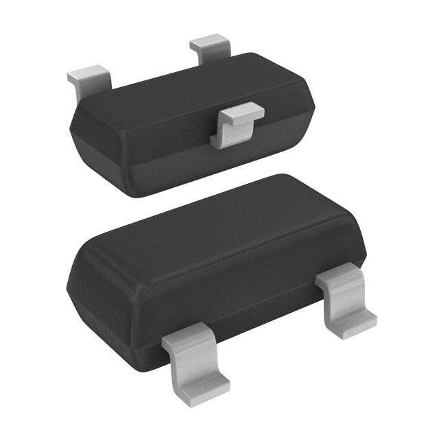
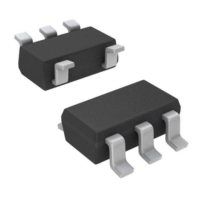
| 产品图片 |
|
| rohs | 符合RoHS无铅 / 符合限制有害物质指令(RoHS)规范要求 |
| 产品系列 | 电源管理 IC,参考电压,Analog Devices ADR130AUJZ-REEL7- |
| 数据手册 | |
| 产品型号 | ADR130AUJZ-REEL7 |
| 产品目录页面 | |
| 产品种类 | 参考电压 |
| 供应商器件封装 | TSOT-6 |
| 其它名称 | ADR130AUJZ-REEL7CT |
| 分流电流—最大值 | 4 mA |
| 初始准确度 | +/- 1.75 mV |
| 包装 | 剪切带 (CT) |
| 参考类型 | 串联,精度 |
| 商标 | Analog Devices |
| 安装类型 | 表面贴装 |
| 安装风格 | SMD/SMT |
| 容差 | ±0.7% |
| 封装 | Reel |
| 封装/外壳 | SOT-23-6 细型,TSOT-23-6 |
| 封装/箱体 | TSOT-6 |
| 工作温度 | -40°C ~ 125°C |
| 工厂包装数量 | 3000 |
| 平均温度系数—典型值 | 5 PPM / C |
| 最大工作温度 | + 125 C |
| 最小工作温度 | - 40 C |
| 标准包装 | 1 |
| 温度系数 | 50ppm/°C |
| 电压-输入 | 2 V ~ 18 V |
| 电压-输出 | 0.5V, 1V |
| 电流-输出 | 4mA |
| 电流-阴极 | - |
| 电流-静态 | 150µA |
| 电源电流 | 150 uA |
| 系列 | ADR130 |
| 输入电压 | 2 V to 18 V |
| 输出电压 | 0.5 V, 1 V |
| 通道数 | 1 |




- 商务部:美国ITC正式对集成电路等产品启动337调查
- 曝三星4nm工艺存在良率问题 高通将骁龙8 Gen1或转产台积电
- 太阳诱电将投资9.5亿元在常州建新厂生产MLCC 预计2023年完工
- 英特尔发布欧洲新工厂建设计划 深化IDM 2.0 战略
- 台积电先进制程称霸业界 有大客户加持明年业绩稳了
- 达到5530亿美元!SIA预计今年全球半导体销售额将创下新高
- 英特尔拟将自动驾驶子公司Mobileye上市 估值或超500亿美元
- 三星加码芯片和SET,合并消费电子和移动部门,撤换高东真等 CEO
- 三星电子宣布重大人事变动 还合并消费电子和移动部门
- 海关总署:前11个月进口集成电路产品价值2.52万亿元 增长14.8%




PDF Datasheet 数据手册内容提取
Precision Series Sub-Band Gap Voltage Reference Data Sheet ADR130 FEATURES PIN CONFIGURATION Initial accuracy NC 1 6 NC A grade: ±0.70% (maximum) ADR130 B grade: ±0.35% (maximum) GND 2 TOP VIEW 5 SET (Not to Scale) MaAx igmraudme :t 5em0 pppemra/t°uCr e coefficient VIN N3C = NO CONNECT4 VOUT 06322-001 B grade: 25 ppm/°C Figure 1. 6-Lead TSOT (UJ-6) CLOAD = 0.1 μF to 1 μF Output current: +4 mA/−2 mA Low operating current: 80 μA (typical) Output noise: 6 μV p-p at 1.0 V output Input range: 2.0 V to 18 V Temperature range: −40°C to +125°C Tiny, Pb-free TSOT package APPLICATIONS Battery-powered instrumentation Portable medical equipment Communication infrastructure equipment GENERAL DESCRIPTION The ADR130 is the first family of tiny, micropower, low voltage, Available in the industrial temperature range of −40°C to high precision voltage references in the industry. Featuring +125°C, the ADR130 is housed in a tiny TSOT package. 0.35% initial accuracy and 25 ppm/°C of temperature drift in For 0.5 V output, tie SET (Pin 5) to V (Pin 4). For 1.0 V OUT the tiny TSOT-23 package, the ADR130 voltage reference only output, tie SET (Pin 5) to GND (Pin 2). requires 80 μA for typical operation. The ADR130 design includes a proprietary temperature drift curvature correction technique that minimizes the nonlinearities in the output voltage vs. temperature characteristics. Rev. D Document Feedback Information furnished by Analog Devices is believed to be accurate and reliable. However, no responsibility is assumed by Analog Devices for its use, nor for any infringements of patents or other One Technology Way, P.O. Box 9106, Norwood, MA 02062-9106, U.S.A. rights of third parties that may result from its use. Specifications subject to change without notice. No license is granted by implication or otherwise under any patent or patent rights of Analog Devices. Tel: 781.329.4700 ©2006–2018 Analog Devices, Inc. All rights reserved. Trademarks and registered trademarks are the property of their respective owners. Technical Support www.analog.com
ADR130 Data Sheet TABLE OF CONTENTS Theory of Operation ...................................................................... 12 Features .............................................................................................. 1 Applications ....................................................................................... 1 Power Dissipation Considerations ........................................... 12 Pin Configuration ............................................................................. 1 Input Capacitor ........................................................................... 12 Output Capacitor ........................................................................ 12 General Description ......................................................................... 1 Application Notes ........................................................................... 13 Revision History ............................................................................... 2 Basic Voltage Reference Connection ....................................... 13 Specifications ..................................................................................... 3 Stacking Reference ICs for Arbitrary Outputs ....................... 13 Electrical Characteristics ............................................................. 3 Absolute Maximum Ratings ............................................................ 5 Precision Current Source .......................................................... 14 Thermal Resistance ...................................................................... 5 Outline Dimensions ....................................................................... 15 ESD Caution .................................................................................. 5 Ordering Guide .......................................................................... 15 Typical Performance Characteristics ............................................. 6 Terminology .................................................................................... 11 REVISION HISTORY 8/2018—Rev. C to Rev. D Change to General Description Section ........................................ 1 Change to Specified Temperature Range Parameter, Table 3 ..... 5 Added Junction Temperature Range Parameter, Table 3 ............ 5 Changes to Ordering Guide .......................................................... 15 3/2013—Rev. B to Rev. C Changes to Figure 34 and Figure 35 ............................................. 13 11/2011—Rev. A to Rev. B Change to C in Features Section .............................................. 1 LOAD Changed 10 µF to 1 µF in Output Capacitor Section ................ 12 Deleted Negative Precision Reference Without Precision Resistors Section ............................................................................. 14 9/2011—Rev. 0 to Rev. A Changes to Lead Temperature (Soldering, 60 sec) Parameter, Table 3 ................................................................................................ 5 10/2006—Revision 0: Initial Version Rev. D | Page 2 of 16
Data Sheet ADR130 SPECIFICATIONS ELECTRICAL CHARACTERISTICS T = 25°C, V = 2.0 V to 18 V, unless otherwise noted. SET (Pin 5) tied to V (Pin 4). A IN OUT Table 1. Parameter Symbol Conditions Min Typ Max Unit OUTPUT VOLTAGE V O A Grade 0.49650 0.5 0.50350 V B Grade 0.49825 0.5 0.50175 V INITIAL ACCURACY ERROR V OERR A Grade −3.50 +3.50 mV B Grade −1.75 +1.75 mV TEMPERATURE COEFFICIENT TCV −40°C < T < +125°C O A A Grade 15 50 ppm/°C B Grade 5 25 ppm/°C LOAD REGULATION −40°C < T < +125°C; 3 V ≤ V ≤ 18 V; −0.13 +0.13 mV/mA A IN 0 mA < I < 4 mA OUT −40°C < T < +125°C; 3 V ≤ V ≤ 18 V; −1.0 +1.0 mV/mA A IN −2 mA < I < 0 mA OUT LINE REGULATION 2.0 V to 18 V, I = 0 mA −40 +10 +40 ppm/V OUT QUIESCENT CURRENT I −40°C < T < +125°C, no load 75 150 µA Q A SHORT-CIRCUIT CURRENT TO GROUND V = 2.0 V 15 mA IN V = 18.0 V 50 mA IN VOLTAGE NOISE 0.1 Hz to 10 Hz 3 µV p-p TURN-ON SETTLING TIME To 0.1%, C = 0.1 µF 80 µs LOAD LONG-TERM STABILITY 1000 hours at 25°C 100 ppm/1000 hours OUTPUT VOLTAGE HYSTERESIS 150 ppm Rev. D | Page 3 of 16
ADR130 Data Sheet T = 25°C, V = 2.0 V to 18 V, unless otherwise noted. SET (Pin 5) tied to GND (Pin 2). A IN Table 2. Parameter Symbol Conditions Min Typ Max Unit OUTPUT VOLTAGE V O A Grade 0.9930 1.0 1.0070 V B Grade 0.9965 1.0 1.0035 V INITIAL ACCURACY ERROR V OERR A Grade −7.0 +7.0 mV B Grade −3.5 +3.5 mV TEMPERATURE COEFFICIENT TCV −40°C < T < +125°C O A A Grade 15 50 ppm/°C B Grade 5 25 ppm/°C LOAD REGULATION −40°C < T < +125°C; 3 V ≤ V ≤ 18 V; −0.25 +0.25 mV/mA A IN 0 mA < I < 4 mA OUT −40°C < T < +125°C; 3 V ≤ V ≤ 18 V; −2.0 +2.0 mV/mA A IN −2 mA < I < 0 mA OUT LINE REGULATION 2.0 V to 18 V, I = 0 mA −40 +10 +40 ppm/V OUT QUIESCENT CURRENT I −40°C < T < +125°C, no load 85 150 µA Q A SHORT-CIRCUIT CURRENT TO GROUND V = 2.0 V 15 mA IN V = 18.0 V 50 mA IN VOLTAGE NOISE 0.1 Hz to 10 Hz 6 µV p-p TURN-ON SETTLING TIME To 0.1%, C = 0.1 µF 80 µs LOAD LONG-TERM STABILITY 1000 hours at 25°C 100 ppm/1000 hours OUTPUT VOLTAGE HYSTERESIS 150 ppm Rev. D | Page 4 of 16
Data Sheet ADR130 ABSOLUTE MAXIMUM RATINGS THERMAL RESISTANCE Table 3. Parameter Ratings θ is specified for the worst-case conditions, that is, a device JA VIN to GND 20 V soldered in a circuit board for surface-mount packages. Internal Power Dissipation 40 mW Storage Temperature Range −65°C to +150°C Table 4. Thermal Resistance Specified Temperature Range −40°C to +125°C Package Type θJA θJC Unit Junction Temperature Range −65°C to +150°C 6-Lead TSOT (UJ-6) 186 67 °C/W Lead Temperature (Soldering, 60 sec) 300°C Stresses at or above those listed under Absolute Maximum ESD CAUTION Ratings may cause permanent damage to the product. This is a stress rating only; functional operation of the product at these or any other conditions above those indicated in the operational section of this specification is not implied. Operation beyond the maximum operating conditions for extended periods may affect product reliability. Rev. D | Page 5 of 16
ADR130 Data Sheet TYPICAL PERFORMANCE CHARACTERISTICS 0.5020 1.004 0.5015 1.003 0.5010 1.002 0.5005 1.001 V) V) (UT0.5000 (UT 1.000 O O V V 0.4995 0.999 0.4990 0.998 00..44998850 06322-002 00..999967 06322-005 –40 –25 –10 5 20 35 50 65 80 95 110 125 –40 –25 –10 5 20 35 50 65 80 95 110 125 TEMPERATURE (°C) TEMPERATURE (°C) Figure 2. VOUT vs. Temperature, VOUT = 0.5 V Figure 5. VOUT vs. Temperature, VOUT = 1 V 10 10 9 9 8 8 S 7 S 7 T T R R PA 6 PA 6 F F R O 5 R O 5 E E MB 4 MB 4 U U N 3 N 3 2 2 01 06322-003 01 06322-006 –50–45–40–35–30–25–20–15–10 –5 0 5 10 15 20 25 30 35 40 45 50 –50–45–40–35–30–25–20–15–10 –5 0 5 10 15 20 25 30 35 40 45 50 TEMPERATURE COEFFICIENT (ppm/°C) TEMPERATURE COEFFICIENT (ppm/°C) Figure 3. Temperature Coefficient, VOUT = 0.5 V Figure 6. Temperature Coefficient, VOUT = 1 V 2.0 2.0 –40°C –40°C +25°C 1.8 1.8 V) 1.6 +125°C +25°C V) 1.6 +125°C (N (N MI MI N_ N_ VI 1.4 VI 1.4 1.2 1.2 1.0 06322-004 1.0 06322-007 –2 –1 0 1 2 3 4 5 –2 –1 0 1 2 3 4 5 LOAD CURRENT (mA) LOAD CURRENT (mA) Figure 4. Minimum Input Voltage vs. Load Current, VOUT = 0.5 V Figure 7. Minimum Input Voltage vs. Load Current, VOUT = 1 V Rev. D | Page 6 of 16
Data Sheet ADR130 160 160 +125°C 140 +125°C 140 A) 120 A) 120 +25°C µ +25°C µ NT ( 100 NT ( 100 –40°C E –40°C E R R UR 80 UR 80 C C Y Y PL 60 PL 60 P P U U S S 40 40 200 06322-008 200 06322-011 2 3 4 5 6 7 8 9 10 11 12 13 14 15 16 17 18 2 3 4 5 6 7 8 9 10 11 12 13 14 15 16 17 18 INPUT VOLTAGE (V) INPUT VOLTAGE (V) Figure 8. Supply Current vs. Input Voltage, VOUT = 0.5 V Figure 11. Supply Current vs. Input Voltage, VOUT = 1 V 6 6 TA = –40°C, +25°C, +125°C TA = –40°C, +25°C, +125°C 5 5 A) A) m m T ( 4 T ( 4 N N E E R R UR 3 UR 3 C C Y Y L L P P P 2 P 2 U U S S 1 1 0 06322-009 0 06322-012 –2 –1 0 1 2 3 4 5 –2 –1 0 1 2 3 4 5 LOAD CURRENT (mA) LOAD CURRENT (mA) Figure 9. Supply Current vs. Load Current, VOUT = 0.5 V Figure 12. Supply Current vs. Load Current, VOUT = 1 V 10 10 VIN = 2V TO 18V VIN = 2V TO 18V 8 8 V) V) m/ m/ p p p p N ( 6 N ( 6 O O TI TI A A L L U U EG 4 EG 4 R R E E N N LI LI 2 2 0 06322-010 0 06322-013 –40 –25 –10 5 20 35 50 65 80 95 110 125 –40 –25 –10 5 20 35 50 65 80 95 110 125 TEMPERATURE (°C) TEMPERATURE (°C) Figure 10. Line Regulation vs. Temperature, VOUT = 0.5 V Figure 13. Line Regulation vs. Temperature, VOUT = 1 V Rev. D | Page 7 of 16
ADR130 Data Sheet 0.05 0.08 A) A) 0.07 m m V/ 0.04 V/ m m 0.06 E ( E ( C C UR 0.03 UR 0.05 O O S S N– N– 0.04 O O LATI 0.02 LATI 0.03 U U G G E E R R 0.02 D 0.01 D A A LO 0 06322-014 LO 0.010 06322-017 –40 –25 –10 5 20 35 50 65 80 95 110 125 –40 –25 –10 5 20 35 50 65 80 95 110 125 TEMPERATURE (°C) TEMPERATURE (°C) Figure 14. Load Regulation (Source) vs. Temperature, VOUT = 0.5 V Figure 17. Load Regulation (Source) vs. Temperature, VOUT = 1 V 1.0 2.0 0.9 1.8 A) A) m 0.8 m 1.6 V/ V/ K (m 0.7 K (m 1.4 N N SI 0.6 SI 1.2 – – N N O 0.5 O 1.0 TI TI A A L 0.4 L 0.8 U U G G RE 0.3 RE 0.6 D D OA 0.2 OA 0.4 L L 0.01 06322-015 0.20 06322-018 –40 –25 –10 5 20 35 50 65 80 95 110 125 –40 –25 –10 5 20 35 50 65 80 95 110 125 TEMPERATURE (°C) TEMPERATURE (°C) Figure 15. Load Regulation (Sink) vs. Temperature, VOUT = 0.5 V Figure 18. Load Regulation (Sink) vs. Temperature, VOUT = 1 V CIN = COUT = 0.1µF CIN = COUT = 0.1µF CH1 PEAK-TO-PEAK 5.72µV CH1 PEAK-TO-PEAK 3.16µV V V DI DI V/ V/ 2µ 2µ 06322-016 06322-019 TIME (1s/DIV) TIME (1s/DIV) Figure 16. 0.1 Hz to 10 Hz Noise, VOUT = 0.5 V Figure 19. 0.1 Hz to 10 Hz Noise, VOUT = 1 V Rev. D | Page 8 of 16
Data Sheet ADR130 PEAK-TO-PEAK CIN = COUT = 0.1µF CIN = COUT = 0.1µF 291µV CH1 PEAK-TO-PEAK 172µV 50µV/DIV 50µV/DIV 06322-020 06322-023 TIME (1s/DIV) TIME (1s/DIV) Figure 20. 10 Hz to 10 kHz Noise, VOUT = 0.5 V Figure 23. 10 Hz to 10 kHz Noise, VOUT = 1 V CIN = COUT = 0.1µF CIN = COUT = 0.1µF VIN = 1V/DIV VIN = 1V/DIV VOUT 200mV/DIV 06322-021 VOUT = 500mV/DIV 06322-024 TIME (40µs/DIV) TIME (40µs/DIV) Figure 21. Turn-On Response, VOUT = 0.5 V Figure 24. Turn-On Response, VOUT = 1 V VIN = 1V/DIV CIN = COUT = 0.1µF CIN = COUT = 0.1µF VIN = 1V/DIV VOUT = 200mV/DIV 06322-022 VOUT = 500mV/DIV 06322-025 TIME (10ms/DIV) TIME (400µs/DIV) Figure 22. Turn-Off Response, VOUT = 0.5 V Figure 25. Turn-Off Response, VOUT = 1 V Rev. D | Page 9 of 16
ADR130 Data Sheet VIN = 1V/DIV CIN = COUT = 0.1µF CIN = COUT = 0.1µF VIN = 1V/DIV VOUT = 20mV/DIV 06322-026 VOUT = 20mV/DIV 06322-029 TIME (100µs/DIV) TIME (100µs/DIV) Figure 26. Line Transient Response, VOUT = 0.5 V Figure 29. Line Transient Response, VOUT = 1 V VLOAD = 0.5V/DIV VLOAD = 1V/DIV CIN = COUT = 0.1µF CIN = COUT = 0.1µF RLOAD = 125Ω RLOAD = 250Ω ILOAD = 0mA ILOAD = 0mA ILOAD = 4mA ILOAD = 4mA VOUT = 20mV/DIV 06322-027 VOUT = 20mV/DIV 06322-030 TIME (40µs/DIV) TIME (40µs/DIV) Figure 27. Load Transient Response (Source), VOUT = 0.5 V Figure 30. Load Transient Response (Source), VOUT = 1 V VLOAD = 200mV/DIV VLOAD = 500mV/DIV CIN = COUT = 0.1µF CIN = COUT = 0.1µF ILOAD = 2mA RLOAD = 125Ω ILOAD = 2mA RLOAD = 250Ω ILOAD = 0mA ILOAD = 0mA VOUT = 100mV/DIV 06322-028 VOUT = 100mV/DIV 06322-031 TIME (40µs/DIV) TIME (40µs/DIV) Figure 28. Load Transient Response (Sink), VOUT = 0.5 V Figure 31. Load Transient Response (Sink), VOUT = 1 V Rev. D | Page 10 of 16
Data Sheet ADR130 TERMINOLOGY Temperature Coefficient Long-Term Stability Temperature coefficient is the change of output voltage with Long-term stability is the typical shift of output voltage at 25°C respect to the operating temperature change normalized by the on a sample of parts subjected to a test of 1000 hours at 25°C. output voltage at 25°C. This parameter is expressed in ppm/°C ∆V =V (t )−V (t ) and is determined by O O 0 O 1 TCV [ppm/°C]= VO(T2)−V(O(T1) )×106 ∆VO [ppm]=VO(tV0)−(tV)O(t1)×106 O V (25°C)× T −T O 0 O 2 1 where: where: V (t) = V at 25°C at Time 0. O 0 O V (25°C) = V at 25°C. O O V (t) = V at 25°C after 1000 hours operating at 25°C. O 1 O V (T) = V at Temperature 1. O 1 O V (T) = V at Temperature 2. Thermal Hysteresis O 2 O Thermal hysteresis is the change of output voltage after the Line Regulation device is cycled through temperatures from +25°C to −40°C to Line regulation is the change in the output due to a specified +125°C, then back to +25°C. This is a typical value from a change in input voltage. This parameter accounts for the effects sample of parts put through such a cycle. of self-heating. Line regulation is expressed in either %/V, ppm/V, or µV/∆V . where: IN V (25°C) = V at 25°C. O O Load Regulation V = V at 25°C after temperature cycle from +25°C to −40°C OTC O Load regulation is the change in output voltage due to a to +125°C, then back to +25°C. specified change in load current. This parameter accounts for the effects of self-heating. Load regulation is expressed in either mV/mA, ppm/mA, or dc output resistance (Ω). Rev. D | Page 11 of 16
ADR130 Data Sheet THEORY OF OPERATION The ADR130 sub-band gap reference is the high performance INPUT CAPACITOR solution for low supply voltage and low power applications. The Input capacitors are not required on the ADR130. There is no uniqueness of this product lies in its architecture. limit for the value of the capacitor used on the input, but a 1 µF POWER DISSIPATION CONSIDERATIONS to 10 µF capacitor on the input improves transient response in applications where there is a sudden supply change. An additional The ADR130 is capable of delivering load currents to 4 mA 0.1 µF capacitor in parallel also helps reduce noise from the supply. with an input range from 3.0 V to 18 V. When this device is used in applications with large input voltages, care must be OUTPUT CAPACITOR taken to avoid exceeding the specified maximum power The ADR130 requires a small 0.1 µF output capacitor for stability. dissipation or junction temperature, because this results in Additional 0.1 µF to 1 µF capacitance in parallel can improve premature device failure. load transient response. This acts as a source of stored energy Use the following formula to calculate the maximum junction for a sudden increase in load current. The only parameter that temperature or dissipation: is affected by the additional capacitance is turn-on time. TJ− TA P = D θ JA where: T is the junction temperature. J T is the ambient temperature. A P is the device power dissipation. D θ is the device package thermal resistance. JA Rev. D | Page 12 of 16
Data Sheet ADR130 APPLICATION NOTES BASIC VOLTAGE REFERENCE CONNECTION 1 NC U2 NC 6 ADR130 The circuits in Figure 32 and Figure 33 illustrate the basic 2 GND SET 5 configuration for the ADR130 voltage reference. 3 VIN VOUT 4 VOUT2 ADR130 0.2µF 1 NC NC 6 0.1µF 2 GND SET 5 INPUT OUTPUT 3 VIN VOUT 4 INPUT 1 NC U1 NC 6 ADR130 0.1µF 0.1µF 06322-032 23 GVINND VSOEUTT 54 VOUT1 Figure 32. Basic Configuration, VOUT = 0.5 V 0.1µF 0.1µF 1 NACDR13N0C 6 06322-035 2 GND SET 5 Figure 35. Stacking References with ADR130, VOUT1 = 0.5 V. VOUT2 = 1.5 V INPUT OUTPUT 3 VIN VOUT 4 Two reference ICs are used and fed from an unregulated input, V . The outputs of the individual ICs that are connected in 0.1µF 0.1µF IN series provide two output voltages, V and V . V is the 06322-033 terminal voltage of U1, and VOUT2 is tOhUeT s1um of OthUTis2 voOltUaTg1e and Figure 33. Basic Configuration, VOUT = 1 V the terminal voltage of U2. U1 and U2 are chosen for the two voltages that supply the required outputs (see Table 5). For STACKING REFERENCE ICs FOR ARBITRARY example, if U1 is set to have an output of 1 V or 0.5 V, the user OUTPUTS can stack on top of U2 to get an output of 2 V or 1.5 V. Some applications may require two reference voltage sources Table 5. Required Outputs that are a combined sum of the standard outputs. Figure 34 and U1/U2 Comments V V Figure 35 show how these stacked output references can be OUT1 OUT2 ADR130/ADR130 See Figure 34 1 V 2 V implemented. ADR130/ADR130 See Figure 35 0.5 V 1.5 V 1 NC U2 NC 6 ADR130 2 GND SET 5 3 VIN VOUT 4 VOUT2 0.2µF 0.1µF INPUT 1 NC U1 NC 6 ADR130 2 GND SET 5 VOUT1 3 VIN VOUT 4 0.1µF 0.1µF 06322-034 Figure 34. Stacking References with ADR130, VOUT1 = 1.0 V, VOUT2 = 2.0 V Rev. D | Page 13 of 16
ADR130 Data Sheet PRECISION CURRENT SOURCE ADR130 1 NC NC 6 In low power applications, the need can arise for a precision 2 GND SET 5 current source that can operate on low supply voltages. The ADR130 can be configured as a precision current source (see VIN 3 VIN VOUT 4 Figure 36). The circuit configuration shown is a floating current RSET source with a grounded load. The reference output voltage is P1 bootstrapped across R , which sets the output current into the SET llooaadd. cWurirtehn tths irsa cnogninfigg ufrroatmio tnh, ec irrecfuerite npcreec siusipopnl yis c murarienntta,i ned for RL 06322-037 typically 85 µA, to approximately 4 mA. Figure 36. ADR130 as a Precision Current Source Rev. D | Page 14 of 16
Data Sheet ADR130 OUTLINE DIMENSIONS 2.90 BSC 6 5 4 2.80 BSC 1.60 BSC 1 2 3 PIN 1 INDICATOR 0.95 BSC 1.90 BSC *0.90 0.87 0.84 0.20 *1.00 MAX 0.08 0.10 MAX SEATING 8° 0.60 0.50 PLANE 4° 0.45 0.30 0° 0.30 *CTOHEM PELXICAENPTT TIOON J OEDFE PCA SCTKAANGDEA HREDISG HMTO A-1N9D3- TAHAICWKINTHESS. 102808-A Figure 37. 6-Lead Thin Small Outline Transistor Package [TSOT] (UJ-6) Dimensions shown in millimeters ORDERING GUIDE Temperature Package Ordering Model1 Coefficient (ppm/°C) Temperature Range Package Description Option Marking Code Quantity ADR130AUJZ-REEL7 50 −40°C to +125°C 6-Lead TSOT UJ-6 R0W 3,000 ADR130BUJZ-REEL7 25 −40°C to +125°C 6-Lead TSOT UJ-6 R0X 3,000 1 Z = RoHS Compliant Part. Rev. D | Page 15 of 16
ADR130 Data Sheet NOTES ©2006–2018 Analog Devices, Inc. All rights reserved. Trademarks and registered trademarks are the property of their respective owners. D06322-0-8/18(D) Rev. D | Page 16 of 16
Mouser Electronics Authorized Distributor Click to View Pricing, Inventory, Delivery & Lifecycle Information: A nalog Devices Inc.: ADR130BUJZ-REEL7 ADR130AUJZ-REEL7 ADR130AUJZ-R2 ADR130BUJZ-R2
 Datasheet下载

