ICGOO在线商城 > 集成电路(IC) > PMIC - 稳压器 - DC DC 开关稳压器 > ADP3050ARZ
 Datasheet下载
- 型号: ADP3050ARZ
- 制造商: Analog
- 库位|库存: xxxx|xxxx
- 要求:
| 数量阶梯 | 香港交货 | 国内含税 |
| +xxxx | $xxxx | ¥xxxx |
查看当月历史价格
查看今年历史价格
ADP3050ARZ产品简介:
ICGOO电子元器件商城为您提供ADP3050ARZ由Analog设计生产,在icgoo商城现货销售,并且可以通过原厂、代理商等渠道进行代购。 ADP3050ARZ价格参考。AnalogADP3050ARZ封装/规格:PMIC - 稳压器 - DC DC 开关稳压器, 可调式 降压,降压升压,SEPIC 开关稳压器 IC 正 1.25V 1 输出 1A(开关) 8-SOIC(0.154",3.90mm 宽)。您可以下载ADP3050ARZ参考资料、Datasheet数据手册功能说明书,资料中有ADP3050ARZ 详细功能的应用电路图电压和使用方法及教程。
ADP3050ARZ 是由 Analog Devices Inc.(ADI)生产的一款 PMIC(电源管理集成电路),具体属于 DC-DC 开关稳压器类别。它具有高效、低功耗和高集成度的特点,适用于多种应用场景。以下是 ADP3050ARZ 的主要应用场景:

 1. 便携式电子设备
   - 应用示例:智能手机、平板电脑、可穿戴设备(如智能手表、健康追踪器)。
   - 特点:ADP3050ARZ 支持宽输入电压范围(2.7V 至 5.5V),适合电池供电的设备。其高效的开关模式可以延长电池寿命,同时保持稳定的输出电压。

 2. 工业自动化
   - 应用示例:传感器模块、数据采集系统、工业控制器。
   - 特点:在工业环境中,ADP3050ARZ 能够提供稳定且高效的电源转换,支持多通道输出配置,满足复杂系统的供电需求。

 3. 通信设备
   - 应用示例:路由器、交换机、基站中的辅助电源模块。
   - 特点:ADP3050ARZ 的小尺寸封装(如 ARZ 封装)使其适合空间受限的设计,同时其高效的性能有助于降低通信设备的功耗。

 4. 汽车电子
   - 应用示例:车载信息娱乐系统、驾驶辅助系统(ADAS)、仪表盘。
   - 特点:该芯片能够在汽车环境中承受较大的电压波动,并提供稳定的电源输出,确保关键系统的正常运行。

 5. 医疗设备
   - 应用示例:便携式医疗仪器(如血糖仪、脉搏血氧仪)、监护设备。
   - 特点:ADP3050ARZ 的低噪声特性和高效率特性非常适合对电源质量要求较高的医疗设备,同时其小型化设计便于集成到紧凑型设备中。

 6. 物联网(IoT)设备
   - 应用示例:智能家居设备、环境监测传感器、无线通信模块。
   - 特点:ADP3050ARZ 的低静态电流和高效能使其成为 IoT 设备的理想选择,能够显著延长电池续航时间。

 总结
ADP3050ARZ 凭借其高效能、低功耗和灵活性,广泛应用于便携式设备、工业自动化、通信设备、汽车电子、医疗设备和物联网等领域。其优异的性能和可靠性,使其成为现代电子系统中不可或缺的电源管理解决方案。
| 参数 | 数值 |
| 产品目录 | 集成电路 (IC)半导体 |
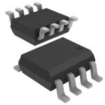
| 描述 | IC REG BUCK ADJ 1A 8SOIC稳压器—开关式稳压器 200kHz 1A Hi-VTG Step-Down |
| 产品分类 | |
| 品牌 | Analog Devices |
| 产品手册 | |
| 产品图片 |
|
| rohs | 符合RoHS无铅 / 符合限制有害物质指令(RoHS)规范要求 |
| 产品系列 | 电源管理 IC,稳压器—开关式稳压器,Analog Devices ADP3050ARZ- |
| 数据手册 | |
| 产品型号 | ADP3050ARZ |
| PWM类型 | 电流模式 |
| 产品种类 | 稳压器—开关式稳压器 |
| 供应商器件封装 | 8-SOIC |
| 包装 | 管件 |
| 同步整流器 | 无 |
| 商标 | Analog Devices |
| 安装类型 | 表面贴装 |
| 安装风格 | SMD/SMT |
| 宽度 | 4 mm (Max) |
| 封装 | Tube |
| 封装/外壳 | 8-SOIC(0.154",3.90mm 宽) |
| 封装/箱体 | SOIC-8 |
| 工作温度 | -40°C ~ 85°C |
| 工厂包装数量 | 98 |
| 开关频率 | 200 kHz |
| 最大工作温度 | + 85 C |
| 最大输入电压 | 30 V |
| 最小工作温度 | - 40 C |
| 最小输入电压 | 3.6 V |
| 标准包装 | 98 |
| 电压-输入 | 3.6 V ~ 30 V |
| 电压-输出 | 1.2 V ~ 30 V |
| 电流-输出 | 1A |
| 类型 | Step Down |
| 系列 | ADP3050 |
| 视频文件 | http://www.digikey.cn/classic/video.aspx?PlayerID=1364138032001&width=640&height=505&videoID=2245193149001 |
| 负载调节 | 1 %/A |
| 输出数 | 1 |
| 输出电压 | Adj |
| 输出电流 | 1 A |
| 输出端数量 | 1 Output |
| 输出类型 | 可调式 |
| 频率-开关 | 200kHz |


- 商务部:美国ITC正式对集成电路等产品启动337调查
- 曝三星4nm工艺存在良率问题 高通将骁龙8 Gen1或转产台积电
- 太阳诱电将投资9.5亿元在常州建新厂生产MLCC 预计2023年完工
- 英特尔发布欧洲新工厂建设计划 深化IDM 2.0 战略
- 台积电先进制程称霸业界 有大客户加持明年业绩稳了
- 达到5530亿美元!SIA预计今年全球半导体销售额将创下新高
- 英特尔拟将自动驾驶子公司Mobileye上市 估值或超500亿美元
- 三星加码芯片和SET,合并消费电子和移动部门,撤换高东真等 CEO
- 三星电子宣布重大人事变动 还合并消费电子和移动部门
- 海关总署:前11个月进口集成电路产品价值2.52万亿元 增长14.8%


PDF Datasheet 数据手册内容提取
200 kHz, 1 A High Voltage Step-Down Switching Regulator Data Sheet ADP3050 FEATURES FUNCTIONAL BLOCK DIAGRAM Wide input voltage range: 3.6 V to 30 V BIAS IN 3 8 Adjustable and fixed (3.3 V, 5 V) output options Integrated 1 A power switch CURRENT SENSE 2.50V AMPLIFIER Uses small surface-mount components SD 6 REGULATOR Cycle-by-cycle current limiting GND 7 Peak input voltage (100 ms): 60 V Configurable as a buck, buck-boost, and SEPIC FREQUENCY CURRENT regulator AND CURRENT LIMIT LIMIT FOLDBACK Available in 8-lead SOIC package Supported by ADIsimPower™ design tool + 200kHz OSCILLATOR APPLICATIONS FB 4 2 BOOST Industrial power systems CMP PC peripheral power systems S Q DRIVER Preregulator for linear regulators R 1 SWITCH Distributed power systems Automotive systems 1.2V gm ADP3050 B attery chargers CO5MP 00125-001 Figure 1. GENERAL DESCRIPTION The ADP3050 is a current mode monolithic buck (step down) The ADP3050 includes a shutdown input that places the device PWM switching regulator that contains a high current 1 A power in a low power mode, reducing the total supply current to under switch and all control, logic, and protection functions. It uses a 20 µA. Internal protection features include thermal shutdown unique compensation scheme allowing the use of any type of circuitry and a cycle-by-cycle current limit for the power switch output capacitor (tantalum, ceramic, electrolytic, OS-CON). to provide complete device protection under fault conditions. Unlike some buck regulators, the design is not restricted to using The ADP3050 provides excellent line and load regulation, a specific type of output capacitor or ESR value. maintaining typically less than ±3% output voltage accuracy A special boosted drive stage is used to saturate the NPN power over temperature and under all input voltage and output switch, providing a system efficiency higher than conventional current conditions. bipolar buck switchers. Further efficiency improvements are The ADP3050 is specified over the industrial temperature range obtained by using the low voltage regulated output to provide of −40°C to +85°C and is available in a thermally enhanced 8-lead the internal operating current of the device. A high switching (not Pb-free only) SOIC package and a standard 8-lead (Pb-free frequency allows the use of small external surface-mount compo- only) RoHS-compliant SOIC package. nents. A wide variety of standard off-the-shelf devices can be used, providing a great deal of design flexibility. A complete regulator design requires only a few external components. Rev. C Information furnished by Analog Devices is believed to be accurate and reliable. However, no responsibility is assumed by Analog Devices for its use, nor for any infringements of patents or other One Technology Way, P.O. Box 9106, Norwood, MA 02062-9106, U.S.A. rights of third parties that may result from its use. Specifications subject to change without notice. No license is granted by implication or otherwise under any patent or patent rights of Analog Devices. Tel: 781.329.4700 www.analog.com Trademarks and registered trademarks are the property of their respective owners. Fax: 781.461.3113 ©2008–2012 Analog Devices, Inc. All rights reserved.
ADP3050 Data Sheet TABLE OF CONTENTS Features .............................................................................................. 1 Catch Diode Selection ............................................................... 13 Applications ....................................................................................... 1 Input Capacitor Selection .......................................................... 14 Functional Block Diagram .............................................................. 1 Discontinous Mode Ringing ..................................................... 14 General Description ......................................................................... 1 Setting the Output Voltage ........................................................ 14 Revision History ............................................................................... 2 Frequency Compensation ......................................................... 14 Specifications ..................................................................................... 3 Current Limit/Frequency Foldback ......................................... 15 Absolute Maximum Ratings ............................................................ 4 Bias Pin Connection .................................................................. 15 ESD Caution .................................................................................. 4 Boosted Drive Stage ................................................................... 15 Pin Configuration and Function Descriptions ............................. 5 Start-Up/Minimum Input Voltage ........................................... 15 Typical Performance Characteristics ............................................. 6 Thermal Considerations ............................................................ 16 Theory of Operation ...................................................................... 10 Board Layout Guidelines ............................................................... 17 Setting the Output Voltage ........................................................ 10 Typical Applications ................................................................... 17 Applications Information .............................................................. 11 Inverting (Buck Boost) Regulator ............................................ 18 ADIsimPower Design Tool ....................................................... 11 Outline Dimensions ....................................................................... 20 Inductor Selection ...................................................................... 11 Ordering Guide .......................................................................... 20 Output Capacitor Selection ....................................................... 12 REVISION HISTORY 6/12—Rev. B to Rev. C Change to Features Section ............................................................. 1 Added ADIsimPower Design Tool Section ................................. 11 Changes to Ordering Guide .......................................................... 20 3/08—Rev. A to Rev. B Updated Format .................................................................. Universal Changes to General Description Section ...................................... 1 Changes to Figure 3 and Figure 5 ................................................... 6 Changes to Table 2 ............................................................................ 4 Deleted Table 4 ................................................................................ 14 Changes to Table 5 .......................................................................... 15 Deleted Table 8 ................................................................................ 15 Deleted Table 7 ................................................................................ 16 Deleted Table 9 ................................................................................ 16 Changes to Boosted Drive Stage Section and Thermal Considerations Sections................................................................. 19 Changes to Figure 27 ...................................................................... 20 Changes to Ordering Guide .......................................................... 23 Rev. C | Page 2 of 20
Data Sheet ADP3050 SPECIFICATIONS V = 10 V, T = −40°C to +85°C, unless otherwise noted. IN A Table 1. Parameter1 Symbol Conditions Min Typ Max Unit FEEDBACK Feedback Voltage V Over line and temperature FB ADP3050 1.16 1.20 1.24 V ADP3050-3.3 3.20 3.30 3.40 V ADP3050-5 4.85 5.00 5.15 V Line Regulation V = 10 V to 30 V, no load 0.005 %/V IN Load Regulation I = 100 mA to 1 A, ADP3050AR only −1.0 +0.1 +1.0 %/A LOAD ADP3050AR-3.3, ADP3050AR-5 −0.5 +0.1 +0.5 %/A Input Bias Current I ADP3050AR only 0.65 2 μA FB ERROR AMPLIFIER Transconductance2 g 1250 μMho m Voltage Gain2 A 300 V/V VOL Output Current ADP3050 COMP = 1.0 V, FB = 1.1 V to 1.3 V ±115 μA ADP3050-3.3 COMP = 1.0 V, FB = 3.0 V to 3.6 V ±120 μA ADP3050-5 COMP = 1.0 V, FB = 4.5 V to 5.5 V ±135 μA OSCILLATOR Oscillator Frequency3 f 170 200 240 kHz OSC Minimum Duty Cycle D 10 % MIN Maximum Duty Cycle D 90 % MAX SWITCH Average Output Current Limit4 I CL(AVG) ADP3050 BOOST = 15 V, FB = 1.1 V 1.0 1.25 1.5 A ADP3050-3.3 BOOST = 15 V, FB = 3.0 V 1.0 1.25 1.5 A ADP3050-5 BOOST = 15 V, FB = 4.5 V 1.0 1.25 1.5 A Peak Switch Current Limit5 I 1.5 1.7 2.1 A CL(PEAK) Saturation Voltage BOOST = 15 V, I = 1 A 0.65 0.95 V LOAD Leakage Current 50 nA SHUTDOWN Input Voltage Low 0.4 V Input Voltage High 2.0 V SUPPLY Input Voltage Range6 V 3.6 30 V IN Minimum BIAS Voltage V 3.0 V BIAS Minimum BOOST Voltage V 3.0 V BOOST IN Supply Current I Q Normal Mode BIAS = 5.0 V 0.7 1.5 mA Shutdown Mode SD = 0 V, VIN ≤ 30 V 15 40 μA BIAS Supply Current I BIAS = 5.0 V 4.0 6.0 mA BIAS BOOST Supply Current I BOOST = 15 V, I = 0.5 A 18 mA BOOST SW BOOST = 15 V, I = 1.0 A 20 40 mA SW 1 All limits at temperature extremes are guaranteed via correlation using standard statistical quality control (SQC). 2 Transconductance and voltage gain measurements refer to the internal amplifier without the voltage divider. To calculate the transconductance and gain of the fixed voltage parts, divide the values shown by FB/1.20. 3 The switching frequency is reduced when the feedback pin is lower than 0.8 × FB. 4 See Figure 24 for typical application circuit. 5 Switch current limit is measured with no diode, no inductor, and no output capacitor. 6 Minimum input voltage is not measured directly, but is guaranteed by other tests. The actual minimum input voltage needed to keep the output in regulation depends on output voltage and load current. Rev. C | Page 3 of 20
ADP3050 Data Sheet ABSOLUTE MAXIMUM RATINGS Table 2. Stresses above those listed under Absolute Maximum Ratings Parameter Rating may cause permanent damage to the device. This is a stress IN Voltage rating only; functional operation of the device at these or any Continuous −0.3 V to +40 V other conditions above those indicated in the operational Peak (<100 ms) −0.3 V to +60 V section of this specification is not implied. Exposure to absolute BOOST Voltage maximum rating conditions for extended periods may affect Continuous −0.3 V to +45 V device reliability. Peak (<100 ms) −0.3 V to +65 V ESD CAUTION SD, BIAS Voltage −0.3 V to IN + 0.3 V FB Voltage −0.3 V to +8 V COMP Voltage −0.3 V to IN + 0.3 V SWITCH Voltage −0.3 V to IN + 0.3 V Operating Ambient Temperature Range −40°C to +85°C Operating Junction Temperature Range −40°C to +125°C Storage Temperature Range −65°C to +150°C θ (4-Layer PCB)1 60.6°C/W JA θ (4-Layer PCB)2 87.5°C/W JA Lead Temperature (Soldering, 60 sec) 300°C 1 Applied to all models that are not Pb-free. 2 Applied to all Pb-free models. Rev. C | Page 4 of 20
Data Sheet ADP3050 PIN CONFIGURATION AND FUNCTION DESCRIPTIONS SWITCH 1 8 IN BOOST 2 ADP3050 7 GND BIAS 3 TOP VIEW 6 SD FB 4 (Not to Scale) 5 COMP 00125-002 Figure 2. Pin Configuration Table 3. Pin Function Descriptions Pin No. Mnemonic Description 1 SWITCH Switch Node. This pin is the emitter of the internal NPN power switch. The voltage at this pin switches between V and approximately −0.5 V. IN 2 BOOST Boost Pin. This pin is used to provide a boosted voltage (higher than V ) for the drive stage of the NPN power IN switch. With the higher drive voltage, the power switch can be saturated, greatly reducing the switch power losses. 3 BIAS Bias Input Pin. Connect this pin to the regulated output voltage to maximize system efficiency. When this pin is above 2.7 V, most of the ADP3050 operating current is taken from the output instead of the input supply. Leave unconnected if not used. 4 FB Feedback Pin. This feedback pin senses the regulated output voltage. Connect this pin directly to the output (fixed output versions). 5 COMP Compensation Node. This pin is used to compensate the regulator with an external resistor and capacitor. This pin is also used to override the control loop. However, the voltage on this pin should not exceed 2 V, because the pin is internally clamped to ensure a fast transient response. Use a pull-up resistor if this pin is to be pulled higher than 2 V. 6 SD Shutdown Pin. Use this pin to turn the device on and off. If this feature is not needed, tie this pin directly to IN. 7 GND Ground Pin. Connect this pin to local ground plane. 8 IN Power Input. Connect this pin to the input supply voltage. An input bypass capacitor must be placed close to this pin to ensure proper regulator operation. Rev. C | Page 5 of 20
ADP3050 Data Sheet TYPICAL PERFORMANCE CHARACTERISTICS 5.0 2.0 VIN = 10V, NO LOAD VIN = 10V A) 4.5 1.8 m G CURRENT ( 343...500 INTO BIAS PIN CURRENT (A)111...462 N T ATI 2.5 PU1.0 PER 2.0 OUT0.8 O E NT 1.5 AG0.6 E R C E ES 1.0 AV0.4 UI Q 0.5 INTO IN PIN 0.2 0–45 –35 –25 –15 –5 TE5MPE1R5AT2U5RE 3(°5C)45 55 65 75 85 00125-003 0–45 –35 –25 –15 –5 TE5MPE1R5AT2U5RE 3(°5C)45 55 65 75 8500125-006 Figure 3. Quiescent Operating Current vs. Temperature Figure 6. Average Output Current Limit vs. Temperature 25 25 A) VIN = 10V µ T (20 20 N E RR A) U m N QUIESCENT C1150 OST CURRENT ( 1150 W O O B D T 5 5 U H S 00 5 1S0UPPLY V1O5LTAGE (V20) 25 30 00125-004 00 0.1 0.2 0.3LO0A.4D CU0R.5REN0T. 6(A) 0.7 0.8 0.9 1.000125-007 Figure 4. Shutdown Quiescent Current vs. Supply Voltage Figure 7. Boost Current vs. Load Current 10 100 VIN = 6V A) BIAS TIED TO VOUT 90 m T ( 8 80 N E RR 70 G CU 6 Y (%) 60 VIN = 12V VIN = 24V ATIN VOUT = 5V ENC 50 VIN = 18V VIN = 30V R CI OPE 4 EFFI 40 T EN VOUT= 3.3V 30 C ES 2 20 L = 33µH UI CIN = 22µF Q 10 COUT = 100µF 00 5 1S0UPPLY V1O5LTAGE (V20) 25 3000125-005 00 200 OUT4P0U0T CURREN60T0 (mA) 800 1k 00125-008 Figure 5. Quiescent Operating Current vs. Supply Voltage Figure 8. 5 V Output Efficiency Rev. C | Page 6 of 20
Data Sheet ADP3050 100 0.6 VIN = 5V VOUT = 3.3V 90 80 %) 0.4 E ( ENCY (%) 675000 VIN = 12VVIN = 1V8IVN = 24VVN = 30V AGE CHANG 0.02 ILOAD = 100mA EFFICI 40 T VOLT 0.2 ILOAD = 1A 30 PU T U 20 L = 33µH O CIN = 22µF 0.4 10 COUT = 100µF 00 200 OUTP40U0T CURREN6T00 (mA) 800 1k00125-009 0.60 10INPUT VOLTAGE (V2)0 30 00125-012 Figure 9. 3.3 V Output Efficiency Figure 12. 3.3 V Output Voltage Change vs. Input Voltage 0.5 8 0.4 VIN = 10V ILOAD = 1A 7 %) 0.3 V) E ( E ( NG 0.2 AG 6 VOUT = 5V A T CH 0.1 OL AGE 0 UT V 5 T P L N VO –0.1 M I PUT –0.2 NIMU 4 VOUT = 3.3V OUT –0.3 MI 3 –0.4 –0.5–45 –35 –25 –15 –5TE5MPE1R5ATU25RE (3°5C) 45 55 65 75 85 00125-010 20 0.1 0.2 0.3 LO0A.4D CU0R.5REN0T.6 (A)0.7 0.8 0.9 1.000125-013 Figure 10. Output Voltage Change vs. Temperature Figure 13. Minimum Input Voltage vs. Load Current 0.6 0 VOUT = 5V VIN = 10V –0.02 E (%) 0.4 E (%) –0.04 G G AN 0.2 AN –0.06 H H C C AGE 0 ILOAD = 1A AGE –0.08 OLT ILOAD = 100mA OLT –0.10 V V UT 0.2 UT –0.12 P P UT UT –0.14 O O 0.4 –0.16 0.60 10INPUT VOLTAGE (V2)0 30 00125-011 –0.180 0.1 0.2 0.3LO0A.4D CU0R.5REN0T.(6A) 0.7 0.8 0.9 1.0 00125-014 Figure 11. 5 V Output Voltage Change vs. Input Voltage Figure 14. Load Regulation Rev. C | Page 7 of 20
ADP3050 Data Sheet 0.8 VIN = 10V V) 0.7 E ( VSW = 5V/DIV G TA 0.6 L O V N 0.5 O 0V TI RA 0.4 SATU 0.3 IL = 500mA/DIV H C VIN = 10V WIT 0.2 VOUT = 5V S 0A ILOAD = 800mA 0.1 L = 33µH CIN = 22µF 00.1 0.2 0.3 0.L4OAD0 .C5URR0E.N6T (A0).7 0.8 0.9 1.0 00125-015 CTOIMUTE =( 11µ0s0/µDFIV) 00125-018 Figure 15. Switch Saturation Voltage vs. Load Current Figure 18. Continuous Conduction Mode Waveforms 210 208 VIN = 10V ILOAD = 250µA Hz)206 VSW = 5V/DIV k Y (204 C N E202 QU 0V VIN = 10V RE200 VOUT = 5V NG F198 LIL O=A 3D3 µ=H 100mA CHI196 CIN = 22µF WIT IL = 500mA/DIV COUT = 100µF S194 0A 192 190–45 –35 –25 –15A–M5BIE5NT T1E5MPE2R5AT3U5RE 4(5°C)55 65 75 85 00125-016 TIME (1µs/DIV) 00125-019 Figure 16. Switching Frequency vs. Temperature Figure 19. Discontinuous Conduction Mode Waveforms 250 VIN = 10V COMP = 0.4V Hz)200 k CY ( 5V VOUT = 200mV/DIV N E150 U Q E R F HING 100 1A ILOAD C SWIT 50 0A VVILIOONUA =TD 1==0 5V1V00mA TO 1A SWITCHED L = 33µH CIN = 22µF 00 0N.O2RMALIZE0D. 4FEEDBACK0 .V6OLTAGE (0V.8) 1.000125-017 COUT = 10T0IµMFE (400µs/DIV) 00125-020 Figure 17. Frequency Foldback Figure 20. Transient Response Rev. C | Page 8 of 20
Data Sheet ADP3050 57.6 220 VIN = 10V 48.0 200 VOUT = 5V RLOAD = 19Ω VOUT = 1V/DIV 38.4 180 L = 33µH COILTRONICS NO LOAD UP2B-330 28.8 160 CIN = 22µF B) s) COUT = 100µF E (d 19.2 140 gree D e AGNITU 9.06 112000 HASE (D M P IL= 500mA/DIV –9.6 80 0V –19.2 60 0A –28.8 40 TIME (100µs/DIV) 00125-021 –38.41 100 FR1kEQUENCY 1(H0zk) 100k 1M20 00125-023 Figure 21. Start-Up from Shutdown Figure 23. Error Amplifier Gain 1500 VIN = 10V, NO LOAD 1450 o) 1400 h M µ 1350 E ( NC 1300 A T C 1250 U D ON 1200 C S N 1150 A R T 1100 1050 1000–45 –35 –25 –15 –5 TE5MPE1R5AT2U5RE 3(°5C)45 55 65 75 85 00125-022 Figure 22. Error Amplifier Transconductance vs. Temperature Rev. C | Page 9 of 20
ADP3050 Data Sheet THEORY OF OPERATION The ADP3050 is a fixed frequency, current mode buck regulator. 3.3V VOUT Current mode systems provide excellent transient response, and +C4 L1 are much easier to compensate than voltage mode systems (refer to 33µH D2 100µF 1N4148 Figure 1). At the beginning of each clock cycle, the oscillator D1 1 SWITCH IN 8 sets the latch, turning on the power switch. The signal at the 1N5818 C3 220nF noninverting input of the comparator is a replica of the switch 2 BOOST GND 7 current (summed with the oscillator ramp). When this signal 3 BIAS SD 6 reaches the appropriate level set by the output of the error amplifier, the comparator resets the latch and turns off the power switch. In 4 FB COMP 5 R1 this manner, the error amplifier sets the correct current trip U1 4kΩ ADP3050-3.3 C2 level to keep the output in regulation. If the error amplifier 1nF 12V output increases, more current is delivered to the output; if it VIN dTehcer ecausrerse,n lte ssse ncuser raemntp ilsif dieerl ipvreorvedid teos tah sei gonuatlp purto. portional to +C221µF 00125-024 switch current to both the comparator and to a cycle-by-cycle Figure 24. Typical Application Circuit current limit. If the current limit is exceeded, the latch is reset, SETTING THE OUTPUT VOLTAGE turning the switch off until the beginning of the next clock The output of the adjustable version (ADP3050AR and cycle. The ADP3050 has a foldback current limit that reduces ADP3050ARZ) can be set to any voltage between 1.25 V and 12 V the switching frequency under fault conditions to reduce stress by connecting a resistor divider to the FB pin as shown in to the IC and to the external components. Figure 25. Most of the control circuitry is biased from the 2.5 V internal V regulator. When the BIAS pin is left open, or when the voltage R2=R1× OUT −1 (1) 1.2 at this pin is less than 2.7 V, all of the operating current for the ADP3050 is drawn from the input supply. When the BIAS pin is L1 22µH above 2.7 V, the majority of the operating current is drawn from 2.5V VOUT this pin (usually tied to the low voltage output of the regulator) D1 +C4 instead of from the higher voltage input supply. This can provide 1N5817 2×22µF CERAMIC substantial efficiency improvements at light load conditions, C3 1 SWITCH IN 8 especially for systems where the input voltage is much higher 0.22µF 2 BOOST GND 7 than the output voltage. CF R2 3 BIAS SD 6 21.5kΩ The ADP3050 uses a special drive stage allowing the power switch to saturate. An external diode and capacitor provide a 4 FB COMP 5 D2 R1 RC boosted voltage to the drive stage that is higher than the input 1N4148 20kΩ U1 7.5kΩ ADP3050 CC supply voltage. Overall efficiency is dramatically improved by 4.7nF using this type of saturating drive stage. 5V VIN Pulling the SD pin below 0.4 V puts the device in a low power +C2×110µF C2 mcuordreen, ts htou tutinndge or f2f0 a lμl Ain. ternal circuitry and reducing the supply GND CERAMIC 0.01µF 00125-025 Figure 25. Adjustable Output Application Circuit Rev. C | Page 10 of 20
Data Sheet ADP3050 APPLICATIONS INFORMATION ADIsimPower DESIGN TOOL The inductor value is calculated using the following equation: The ADP3050 is supported by the ADIsimPower design tool set. V −V 1 V L= IN(MAX) OUT × × OUT (2) ADIsimPower is a collection of tools that produce complete power I f V RIPPLE SW IN(MAX) designs optimized for a specific design goal. The tools enable the user to generate a full schematic, bill of materials, and calculate Where VIN(MAX) is the maximum input voltage, VOUT is the performance in minutes. ADIsimPower can optimize designs for regulated output voltage, and fSW is the switching frequency cost, area, efficiency, and parts count while taking into considera- (200 kHz). The initial choice for the amount of ripple current tion the operating conditions and limitations of the IC and all real may seem arbitrary, but it serves as a good starting point for external components. For more information about ADIsimPower finding a standard off-the-shelf inductor value, such as design tools, refer to www.analog.com/ADIsimPower. The tool 10 μH, 15 μH, 22 μH, 33 μH, and 47 μH. If a specific inductance set is available from this website, and users can request an value is to be used, simply rearrange Equation 2 to find the unpopulated board through the tool. ripple current. For an 800 mA, 12 V to 5 V system, and a ripple current of 320 mA (40% of 800 mA) is chosen, the inductance is The complete process for designing a step-down switching regulator using the ADP3050 is provided in the following 12−5 1 5 L= × × =45.5μH sections. Each section includes a list of recommended devices. 0.32 200×103 12 These lists do not include every available device or manufacturer. A 47 μH inductor is the closest standard value that gives a ripple They contain only surface-mount devices. Equivalent through- current of about 310 mA. The peak switch current is equal to hole devices can be substituted if needed. In choosing components, the load current plus one-half the ripple current (this is also the keep in mind what is most important to the design, for example, peak current for the inductor and the catch diode). efficiency, cost, and size. These ultimately determine which compo- nents are used. It is also important to ensure that the design I =I +1I =0.8+0.155=0.95A (3) specifications are clearly defined and reflect the worst-case SW(PK) OUT(MAX) 2 RIPPLE conditions. Key specifications include the minimum and Pick an inductor with a dc (or saturation) current rating about 20% maximum input voltage, the output voltage and ripple, and the larger than I to ensure that the inductor is not running near SW(PK) minimum and maximum load current. the edge of saturation. For this example, 1.20 × 0.95 A = 1.14 A, use INDUCTOR SELECTION an inductor with a dc current rating of at least 1.2 A. The maxi- mum switch current is internally limited to 1.5 A, and this limit, The inductor value determines the mode of operation for the along with the ripple current, determines the maximum load regulator: continuous mode, where the inductor current flows current the system can provide. continuously; or discontinuous mode, where the inductor current reduces to zero during every switch cycle. Continuous mode is If the load current decreases to below one-half the ripple the best choice for many applications. It provides higher output current, the regulator operates in discontinuous mode. power, lower peak currents in the switch, inductor, and diode, Discontinuous Mode and a lower inductor ripple current, which means lower output For load currents less than approximately 0.5 A, discontinuous ripple voltage. Discontinuous mode allows the use of smaller mode operation can be used. This allows the use of a smaller magnetics, but at a price: lower available load current and inductor, but the ripple current is much higher (which means a higher peak and ripple currents. Designs with a high input higher output ripple voltage). If a larger output capacitor must voltage or a low load current often operate in discontinuous be used to reduce the output ripple voltage, the overall system mode to minimize inductor value and size. The ADP3050 is may take up more board area than if a larger inductor is used. designed to work well in both modes of operation. The operation and equations for the two modes are quite different, Continuous Mode but the boundary between these two modes occurs when the ripple The inductor current in a continuous mode system is a triangular current is equal to twice the load current (when IRIPPLE = 2 × IOUT). waveform (equal to the ripple current) centered around a dc From this, Equation 2 is used to find the minimum inductor value (equal to the load current). The amount of ripple current value needed to keep the system in continuous mode operation is determined by the inductor value, and is usually between 20% (solve for the inductor value with IRIPPLE = 2 × IOUT). and 40% of the maximum load current. To reduce the inductor V −V 1 V size, ripple currents between 40% and 80% are often used in LDIS= IN(2M×AXI) OUT × f ×V OUT (4) continuous mode designs with a high input voltage or a low OUT SW IN(MAX) output current. Using an inductor below this value causes the system to operate in discontinuous mode. Rev. C | Page 11 of 20
ADP3050 Data Sheet For a 400 mA, 24 V to 5 V system in the Inductor Selection section). Contact the manufacturers 24−5 1 5 for their full product offering, availability, and pricing. The L ≤ × × ≤24.7μH manufacturers offer many more values and package sizes to suit DIS 2×0.4 200×103 24 numerous applications. If the chosen inductor value is too small, the internal current 1. Choose a mode of operation, then calculate the inductor limit trips each cycle and the regulator has trouble providing the value using the appropriate equation. For continuous mode necessary load current. systems, a ripple current of 40% of the maximum load current Inductor Core Types and Materials is a good starting point. The inductor value can then be increased or decreased, if desired. Many types of inductors are currently available. Numerous core 2. Calculate the peak switch current (this is the maximum styles along with numerous core materials often make the selection current seen by the inductor). Make sure that the dc (or process seem even more confusing. A quick overview of the saturation) current rating of the inductor is high enough types of inductors available makes the selection process a little (around 1.2× the peak switch current). Inductors with dc easier to understand. current ratings of at least 1 A should be used for all Open core geometries (bobbin core) are usually less expensive designs. This provides a safety margin for start-up and than closed core geometries (toroidal core) and are a good choice fault conditions where the inductor current is higher than for some applications, but care must be taken when they are normal. If the current rating of an inductor is exceeded, the used. In open core inductors, the magnetic flux is not completely core saturates, causing the inductance value to decrease contained inside the core. The radiating magnetic field generates and the temperature of the inductor to increase. electromagnetic interference (EMI), often inducing voltages 3. Estimate the dc winding resistance based on the inductance onto nearby circuit board traces. These inductors may not be value. A general rule is to allow approximately 5 mΩ of suitable for systems that contain very high accuracy circuits or resistance per μH of inductance. sensitive magnetics. A few manufacturers have semiclosed and 4. Pick the core material and type. First, decide if an open- shielded cores, where an outer magnetic shield surrounds a core inductor can be used with the design. If this cannot be bobbin core. These devices have less EMI than the standard determined, try a few samples of each type (open core, open core and are usually smaller than a closed core. semi closed core, shielded core, and closed core). Do not be Most core materials used in surface-mount inductors are either discouraged from using open core inductors because they powdered iron or ferrite. For many designs, material choice is require extra care; just be aware of what to look for if used. arbitrary, but the properties of each material should be recognized. They are quite small and inexpensive, and are used Ferrites have lower core losses than powdered iron, but the successfully in many different applications. lower loss means a higher price. Powdered iron cores saturate OUTPUT CAPACITOR SELECTION softly (the inductance gradually reduces as current rating is exceeded), whereas ferrite cores saturate much more abruptly The ADP3050 can be used with any type of output capacitor. (the inductance rapidly reduces). Kool Mμ® is one type of ferrite The trade-offs between price, component size, and regulator that is specially designed to minimize core losses and heat performance can be evaluated to determine the best choice for generation (especially at switching frequencies above 100 kHz), each application. The effective series resistance (ESR) of the but again, these devices are more expensive. capacitor plays an important role in both the loop compensation and the system performance. The ESR provides a 0 in the The winding dc resistance (DCR) of the inductor must not be feedback loop; therefore, the ESR value must be known so the overlooked. A high DCR can decrease system efficiency by 2% loop can be compensated correctly (most manufacturers specify to 5% for lower output voltages at heavy loads. To obtain a maximum ESR in their data sheets). The capacitor ESR also lower DCR means using a physically larger inductor, so a trade- contributes to the output ripple voltage (V = ESR × I ). off in size and efficiency must be made. The power loss due to this RIPPLE RIPPLE Solid tantalum or multilayer ceramic capacitors are recommended, resistance is I 2 × DCR. For an 800 mA, 5 V to 3.3 V system OUT providing good performance with a small size and reasonable cost. with an inductor DCR of 100 mΩ, the winding resistance dissipates Solid tantalum capacitors have a good combination of low ESR (0.82 A)2 × 0.1 Ω = 64 mW. This represents a power loss to the and high capacitance, and are available from several different system of 64 mW/(3.3 V × 800 mA) = 2.4%. Typical DCR manufacturers. Capacitance values from 22 μF to more than 500 μF values are between 10 mΩ and 200 mΩ. can be used, but values of 47 μF to 220 μF are sufficient for most designs. A smaller value can be used, but ESR is size-dependent, Choosing an Inductor so a smaller device has a higher ESR. Ensure that the ripple Several considerations must be made when choosing an inductor: current of the capacitor rating is larger than the inductor ripple cost, size, EMI, core and copper losses, and maximum current current (the ripple current flows into the output capacitor). rating. Use the following steps to choose an inductor that is Multilayer ceramic capacitors can be used in applications where right for the system (refer to the calculations and descriptions minimum output voltage ripple is a priority. They have a very Rev. C | Page 12 of 20
Data Sheet ADP3050 low ESR (a 22 μF ceramic can have an ESR one-fifth that of a 1 A) and fast switching speed of a Schottky rectifier provide the 22 μF solid tantalum), but may require more board area for the best performance and efficiency. The 1N5818 is rated at 30 V same value of output capacitance. A few manufacturers have reverse voltage and 1 A average forward current. For lower recently improved upon their low voltage ceramic capacitors, input voltages, use a lower voltage Schottky to reduce the diode providing a smaller package with a lower ESR (NEC Tokin, forward voltage drop and increase overall system efficiency; for Murata, Taiyo Yuden, and AVX). Several ceramics can be used example, a 12 V to 5 V system does not need a 30 V diode. For in parallel to give an extremely low ESR and a good value of automotive applications, a 60 V Schottky may be necessary. The capacitance. If the design is cost sensitive and not severely space average forward current for the catch diode is calculated by limited, several aluminum electrolytic capacitors can be used in V −V parallel (their size and ESR are larger than ceramic and solid I =I × IN OUT (5) DIODE(AVG) OUT V tantalum). OS-CON capacitors can also be used, but they are IN typically larger and more expensive than ceramic or solid For the earlier continuous mode example (12 V to 5 V at tantalum capacitors. 800 mA), the average diode current is Choosing an Output Capacitor 12−5 I =0.8× =0.47A (6) Use the following steps to choose an appropriate capacitor. DIODE(AVG) 12 1. Decide the maximum output ripple voltage for the design, For this system, a 1N5817 is a good choice (rated at 20 V and 1 A). and this determines your maximum ESR (remember that Do not use catch diodes rated less than 1 A. Even though the V ≈ ESR × I ). Typical output ripple voltages range average current can be less than 1 A under normal operating RIPPLE RIPPLE between 0.5% and 2% of the output voltage. To lower the conditions, as the diode current is much higher under fault output voltage ripple, there are only two choices: either conditions. The worst-case fault condition for the diode occurs increase the inductor value, or use an output capacitor with when the regulator becomes slightly overloaded (sometimes a lower ESR. called a soft short). This is usually only a problem when the 2. Decide what type of capacitor to use (tantalum, ceramic, or input voltage to output voltage ratio is greater than 2.5. Under others). Many more values, sizes, and voltage ratings are this condition, the load current needed is slightly more than the available, so contact each manufacturer for a complete regulator can provide. The output voltage droops slightly, and product list. If a certain type of capacitor must be used and the switch stays on every cycle until the internal current limit is space permits, use several devices in parallel to reduce the reached. Under this condition, the load current can reach total ESR. around 1.2 A. For example, when using a system with an input 3. Check the capacitor voltage rating and ripple current rating voltage of 24 V and an output voltage of 5 V, if a gradual overload to ensure it works for the application in question. These causes the output voltage to droop to 4 V, the average diode ratings are derated for higher temperatures, so always check current is the manufacturer’s data sheet. 24−4 4. Make sure the final choice for the output capacitor has I =1.2× =1.0A (7) DIODE(AVG) 24 been optimized for cost, size, availability, and performance If the system must survive such gradual overloads for a prolonged yet still meets the required capacitance. The recommended period of time, ensure the diode chosen can survive these capacitance is in the 47 μF to 220 μF range. conditions. A larger 2 A or 3 A diode can be used if necessary. CATCH DIODE SELECTION The recommended catch diode is a Type 1N5818 Schottky or equivalent. The low forward voltage drop (450 mV typical at Table 4. Manufacturers Inductor Manufacturers Capacitor Manufacturers Schottky Diode Manufacturers Sumida AVX Motorola Coilcraft Kemet Diodes, Inc. Cooper Bussmann Coiltronics Murata International Rectifier NEC Tokin Nemco Nihon Inter Electronics Würth Elektronik Vishay Sprague Toko NEC Tokin Taiyo Yuden Rev. C | Page 13 of 20
ADP3050 Data Sheet Choosing a Catch Diode DISCONTINOUS MODE RINGING Use the following steps to pick an appropriate catch diode. When operating in discontinuous mode, high frequency Table 5 shows several Schottky rectifiers with different reverse ringing appears at the switch node when the inductor current voltage and forward current ratings. has decreased to zero. This ringing is normal and is not a result The average diode current rating must be sufficient to provide of loop instability. It is caused by the switch and diode capacitance the required load current (see the calculations in the previous reacting with the inductor to form a damped sinusoidal ringing. section). Diodes rated below 1 A should not be used, even if the This ringing is usually in the range of several megahertz, and is average diode current is much lower. not harmful to normal circuit operation. SETTING THE OUTPUT VOLTAGE The reverse voltage rating of the catch diode should be at least the maximum input voltage. Often a higher rating is chosen The fixed voltage versions of the ADP3050 (3.3 V and 5 V) have (1.2× the maximum input voltage) to provide a safety margin. the feedback resistor divider included on-chip. For the adjustable version, the output voltage is set using two external resistors. Table 5. Schottky Diode Selection Guide Referring to Figure 25, pick a value for R1 between 10 kΩ and V 1 A 2 A 3 A R 20 kΩ, then calculate the appropriate value for R2 using the 15 V 10BQ15 30BQ15 following equation: 20 V 1N5817 B220 SK32 30 V V1N5818 B230 SK33 R2=R1×VOUT −1 (9) 40 V 1N5819 B240 SK34 1.20 INPUT CAPACITOR SELECTION It is important to note that the accuracy of these resistors directly affects the accuracy of the output voltage. The FB pin The input bypass capacitor plays an important role in proper threshold variation is ±3%, and the tolerances of R1 and R2 add regulator operation, minimizing voltage transients at the input to this to determine the total output variation. Use 1% resistors and providing a short local loop for the switching current. Place placed close to the FB pin to prevent noise pickup. this capacitor close to the ADP3050 between the IN and GND pins using short, wide traces. This input capacitor should have FREQUENCY COMPENSATION an rms ripple current rating of at least The ADP3050 uses a unique compensation scheme that allows V V 2 the use of any type of output capacitor. The designer is not ICIN(RMS)≥IOUT× VOIUNT − VOIUNT (8) lEimxtietrenda tlo c oam sppeecnifsiact itoynp ea lolof wcasp tahcei tdoers oigrn ae srp teoc oifpict iEmSiRze r tahneg elo. op for transient response and system performance. The values for This rating is crucial because the input capacitor must be able to R and C set the pole and zero locations for the error amplifier withstand the large current pulses present at the input of a step- C C to compensate the regulator loop. down regulator. Values of 20 μF to 50 μF are typical, but the main criteria for capacitor selection is the ripple current and For tantalum output capacitors, the typical system compensation voltage ratings. values are R = 4 kΩ and C = 1 nF; for ceramics, the typical C C values are R = 4 kΩ and C = 4.7 nF. These values may not be Ceramics are an excellent choice for input bypassing, due to C C optimized for all designs, but they provide a good starting point for their low ESR and high ripple current rating. Ceramics are selecting the final compensation values. Other types of output especially suited for high input voltages and are available from capacitors require different values of C between 0.5 nF and 10 nF. many different manufacturers. Tantalums are often used for C Typically, the lower the ESR of the output capacitor, the larger input bypassing, but precautions must be taken because they the value for C . Normal variations in capacitor ESR, output occasionally fail when subjected to large inrush currents during C capacitance, and inductor value (due to production tolerances, power-up. These surges are common when the regulator input changes in operating point, changes in temperature) affect the is connected to a battery or high capacitance supply. Several loop gain and phase response. Always check the final design manufacturers now offer surface-mount solid tantalum capacitors over its complete operating range to ensure proper regulator that are surge tested, but even these devices can fail if the current operation. surge occurs when the capacitor voltage is near its maximum rating. For this reason, a 2:1 derating is suggested for tantalum Adjusting the R and C values can optimize compensation. Use C C capacitors used in applications where large inrush currents are the typical values above as a starting point, then try increasing present. For example, a 20 V tantalum should be used only for and decreasing each independently and observing the transient an input voltage up to 10 V. Aluminum electrolytics are the response. An easy way to check the transient response of the cheapest choice, but it takes several in parallel to get a good rms design is to observe the output while pulsing the load current at current rating. OS-CON capacitors have a good ESR and ripple a rate of approximately 100 Hz to 1 kHz. There should be some current rating, but they are typically larger and more costly. slight ringing at the output when the load pulses, but this should Refer to Table 4 for a list of capacitor manufacturers. not be excessive (just a few rings). The frequency of this ringing Rev. C | Page 14 of 20
Data Sheet ADP3050 shows the approximate unity-gain frequency of the loop. Again, BIAS PIN CONNECTION always check the design over its full operating range of input To help improve efficiency, most of the internal operating voltage, output current, and temperature to ensure that the loop current can be drawn from the lower voltage regulated output is compensated correctly. voltage instead of the input supply. For example, if the input In addition to setting the zero location, RC also sets the high voltage is 24 V and the output voltage is 5 V, a quiescent current frequency gain of the error amplifier. If this gain is too large, of 4 mA wastes 96 mW if drawn from the input supply, but only output ripple voltage appears at the COMP pin (the output of 20 mW is drawn from the regulated 5 V output. This power the error amplifier) with enough amplitude to interfere with savings is most evident at high input voltages and low load normal regulator operation. If this occurs, subharmonic switching currents. The output voltage must be 3 V or higher to take results (the pulse width of the switch waveform changes, even advantage of this feature. though the output voltage stays regulated). The voltage ripple at the BOOSTED DRIVE STAGE COMP pin should be kept below 100 mV to prevent subharmonic An external capacitor and diode are used to provide the boosted switching from occurring. The amount of ripple can be estimated voltage needed for the special drive stage. If the output voltage is by the following formula, where g is the error amplifier m above 4 V, connect the anode of the boost diode to the regulated transconductance (g = 1250 μMho): m output; for output voltages less than or equal to voltages of ≤3 V, ( ) ( ) V V = g ×R × I ×ESR × FB (10) connect it to the input supply. For some low voltage systems, COMP,RIPPLE m C RIPPLE V OUT such as 5 V to 3.3 V converters, the anode of the boost diode For example, a 12 V to 5 V, 800 mA regulator with an inductor of can be connected to either the input or output voltage. During L = 47 μH has I = 310 mA (see example from the Continuous switch off time, the boost capacitor is charged up to the voltage RIPPLE Mode section) if a 100 μF tantalum output capacitor with a at the anode of the boost diode. When the switch turns on, this maximum ESR of 100 mΩ and compensation values of R = 4 kΩ voltage is added to the switch voltage (the boost diode is reverse- C and C = 1 nF are used. The ripple voltage at the COMP pin is biased), providing a voltage higher than the input supply. The C peak voltage appearing on the BOOST pin is the sum of the VCOMP,RIPPLE=(1250×10−6×4×103)×(0.310×0.1)×15.2.00 (11) input voltage and the boost voltage (either VIN + VOUT or 2 × VIN). Ensure that this peak voltage does not exceed the BOOST pin =37.2mV maximum rating of 45 V. If this ripple voltage is more than 100 mV, RC needs to be For most applications, a 1N4148 or 1N914 type diode can be decreased to prevent subharmonic switching. Typical values for used with a 220 nF capacitor. A 470 nF capacitor may be needed RC are in the range of 2 kΩ to 10 kΩ. for output voltages between 3 V and 4 V. The boost capacitor For output voltages greater than 5 V, it may be necessary to add should have an ESR of less than 2 Ω to ensure that it is adequately a small capacitor in parallel with R2, as shown in Figure 25. charged up during switch off time. Almost any type of film or This improves stability and transient response. For tantalum ceramic capacitor can be used. output capacitors, the typical value for CF is 100 pF. For ceramic START-UP/MINIMUM INPUT VOLTAGE output capacitors, the typical value for C is 400 pF. F For most designs, the regulated output voltage provides the CURRENT LIMIT/FREQUENCY FOLDBACK boosted voltage for the drive stage. During startup, the output The ADP3050 uses a cycle-by-cycle current limit to protect the voltage is 0, so there is no boosted supply for the drive stage. device under fault and high stress conditions. When the current To deal with this problem, the ADP3050 contains a backup drive limit is exceeded, the power switch turns off until the beginning stage to get everything started. As the output voltage increases, of the next oscillator cycle. If the voltage on the feedback pin so does the boost voltage. When the boost voltage reaches approx- drops below 80% of its nominal value, the oscillator frequency imately 2.5 V, the switch drives transition smoothly from the starts to decrease (see Figure 17 in the Typical Performance backup driver to the boosted driver. If the boost voltage decreases Characteristics section). The frequency gradually reduces to a below approximately 2.5 V, resulting in a short-circuit or minimum value of approximately 80 kHz (this minimum overload condition, the backup stage takes over to provide switch occurs when the feedback voltage falls to 30% of its nominal drive. The minimum input voltage needed for the ADP3050 to value). This reduces the power dissipation in the IC, the function correctly is about 3.6 V (this ensures proper operation of external diode, and the inductor during short-circuit the internal circuitry), but a small amount of headroom is needed conditions. This frequency foldback method provides complete for all step-down regulators. The following formula gives the device fault protection without interfering with the normal approximate minimum input voltage needed for a given system, device operation. where V is the switch saturation voltage (see Figure 15 for the SAT appropriate value of VSAT). Figure 13 also shows the typical minimum input voltage needed for 3.3 V and 5 V systems. Rev. C | Page 15 of 20
ADP3050 Data Sheet V +V 3.3 V = OUT SAT (12) P =0.8×0.6× + IN(MIN) 0.85 SW 5.0 THERMAL CONSIDERATIONS (50×10−9×0.8×5.0×200×103)=357mW Several factors contribute to IC power dissipation: ac and dc 0.8 3.32 P = × =35mW switch losses, boost current, and quiescent current. The following BOOST 50 5.0 formulas are used to calculate these losses to determine the power P =(5×10⁻³)+(3.3×4×10−3)=18mW Q dissipation of the IC. These formulas assume continuous mode For a total IC power dissipation of operation, but they provide a reasonable estimate for disconti- nuous mode systems (do not use these formulas to calculate P =P +P +P =410mW (16) TOTAL SW BOOST Q efficiency at light loads). The ADP3050 is offered in a thermally enhanced (not Pb-free) Switch loss 8-lead SOIC package with a thermal resistance, θ , of 60.6°C/W, JA V ( ) and in a standard Pb-free 8-lead SOIC package with θJA of PSW=IOUT×VSAT× VOUT + tOV×IOUT×VIN×fSW (13) 87.5°C/W. IN The maximum die temperature, T, is calculated using the J Boost current loss thermal resistance and the maximum ambient temperature P =IOUT ×VOUT2 (14) TJ =TA+θJA×PTOTAL (17) BOOST β V SW IN For the previous example (5 V to 3.3 V at 800 mA system, Pb- Quiescent current loss free 8-lead SOIC package using good layout techniques) with a P =(V ×I )+(V ×I ) (15) worst-case ambient temperature of 70°C Q IN Q OUT BIAS T = 70°C + 87.5°C/W × 0.41 = 105.9°C where: J V is ~0.6 V at I = 800 mA (taken from Figure 15). The maximum operating junction (die) temperature is 125°C, SAT OUT f is the switch frequency (200 kHz). therefore this system operates within the safe limits of the SW t is the switch current/voltage overlap time (~50 ns). ADP3050. Check the die temperature at minimum and OV β is the current gain of the NPN power switch (~50). maximum supply voltages to ensure proper operation under all SW I is the quiescent current drawn from V (~1 mA). conditions. Although the PCB and its copper traces provide Q IN I is the quiescent current drawn from V (~4 mA). sufficient heat sinking, it is important to follow the layout BIAS OUT suggestions in the Board Layout Guidelines section. For any For example, a 5 V to 3.3 V system with I = 800 mA OUT design that combines high output current with high duty cycle and/or high input voltage, the junction temperature must be calculated to ensure normal operation. Always use the equations in this section to estimate the power dissipation. Rev. C | Page 16 of 20
Data Sheet ADP3050 BOARD LAYOUT GUIDELINES A good board layout is essential when designing a switching regulator. The high switching currents along with parasitic wiring inductances can generate significant voltage transients OUTPUT GROUND INPUT and cause havoc in sensitive circuits. For best results, keep the main switching path as tight as possible (keep L1, D1, C , and IN C1 C close together) and minimize the copper area of the SWITCH OUT and BOOST nodes (without violating current density require- ments) to reduce the amount of noise coupling into other sensitive nodes. L1 L1 C3 VIN IN SWITCH VOUT ADP3050 CIN D1 COUT D1 GND D2 C2 GND GND 00125-026 The external compoFingeunret s2 6s.h Moauinld S wbeit clhoicnagt Peadt ha s close to the R2 R1 CCADP305R0C 00125-027 ADP3050 as possible. For best thermal performance, use wide Figure 27. Recommended Board Layout copper traces for all IC connections, and always connect the GND pin to a large piece of copper or ground plane. The additional L1 copper improves heat transfer from the IC, greatly reducing the 22µH 3.3V package thermal resistance. Further improvements of the thermal VOUT D1 D2 +C5 performance can be made by using multilayer boards and using 1N5817 1N4148 100µF 1 SWITCH IN 8 vias to transfer heat to the other layers. A single layer board C3 0.22µF layout is shown in Figure 27. The amount of copper used for the 2 BOOST GND 7 input, output, and ground traces can be reduced, but were made 3 BIAS SD 6 large to improve the thermal performance. For the 5 V and 3.3 V versions, leave out R1 and R2; for the adjustable version, remove 4 FB COMP 5 R1 the trace that shorts out R2. Route all sensitive traces and compo- U1 7.5kΩ nents, such as those associated with feedback and compensation, ADP3050-3.3 C1n4F away from the BOOST and SWITCH traces. SD TYPICAL APPLICATIONS 5V VIN 5 V to 3.3 V Buck (Step-Down) Regulator +C1 C2 22µF 0.01µF Tcohnef icgirucruaitti oinn .F Iitg ius rues 2e8d stho ogwens etrhaet eA 3D.3P V30 r5e0g iunl aat ebdu ocku tput from GND 00125-028 5 V input voltage with the following specifications: Figure 28. 5 V to 3.3 V Buck Regulator V = 4.5 V to 5.5 V IN V = 3.3 V OUT I = 0.75 A OUT I = 0.4 A × 0.75 A = 0.3 A RIPPLE V = 50 mV OUT_RIPPLE Rev. C | Page 17 of 20
ADP3050 Data Sheet INVERTING (BUCK BOOST) REGULATOR For the circuit in Figure 29, the maximum ripple current (at the maximum input voltage) is The circuit in Figure 29 shows the ADP3050 in a buck-boost configuration that produces a negative output voltage from a I = 12 × 1 × −5 =0.375A positive input voltage. This topology looks quite similar to the RIPPLE 47×10−6 200×103 12+−5 buck shown in Figure 28 (except the IC and the output filter are High ripple currents are present in both the input and output now referenced to the negative output instead of ground), but capacitors, and their ripple current ratings must be large its operation is quite different. For this topology, the feedback enough to sustain the large switching currents present in this pin is grounded and the GND pin is tied to the negative output, topology. The capacitors should have a ripple current rating of allowing the feedback network of the IC to regulate the negative at least output voltage. V 47µLH1 1N41D482 100CµF5 + IRMS(CIN,COUT)≈IOUT× VOIUNT (20) 1 SWITCH IN 8 C3 The peak current seen by the diode, switch, and inductor is 0.22µF 2 BOOST GND 7 found by rearranging the load current equation D1 1N5818 3 BIAS SD 6 I =VIN +VOUT ×I +1×I (21) 4 FB COMP 5 PEAK VIN OUT 2 RIPPLE R1 U1 5.1kΩ ADP3050-5 C4 The largest peak currents occur at the lowest input voltage. For 3.3nF VOUT this design with a load current of 500 mA SD –5V AT 0.5A VIN12V +C1 C2 IPEAK =12+12−5×0.5+21×0.375=0.9A (22) GND 22µF 0.01µF 00125-029 The average current diode is equal to the load current. An inductor with a current rating 20% greater than 0.9 A Figure 29. Inverting (Buck-Boost) Regulator should be used (a rating of at least 1.2 A). Inductors and diodes The design procedure used for the standard buck converter with ratings greater than 1 A should always be used, even if cannot be used for a buck-boost converter due to fundamental the calculated peak and average currents are lower. This ensures differences in how the output voltage is generated. The switch that start-up and fault conditions do not overstress the currents in the buck-boost are much higher than the standard components. buck converter, thus lowering the available load current. To For the buck-boost topology, the input voltage can be less than calculate the maximum output current for a given maximum the output voltage, such as V = 4 V or V = −5 V, but the IN OUT switch current, use the following equation: available load current is even lower. The equations given in this I = VIN × section are valid for input voltages less than and greater than OUT(MAX) V +V the output voltage. The voltage seen by the ADP3050 is equal to IN OUT (18) the sum of the input and output voltages (the BOOST pin sees V ×V I − IN ( OUT ) the sum of VIN + 2 × |VOUT|). It is important to ensure that the SW(MAX) 2×fSW×L×VIN +VOUT maximum voltage rating of these pins is not exceeded. where I is the switch current limit rating of the ADP3050, SW(MAX) and V is the minimum input voltage. The inductor ripple IN current is estimated using the following equation: V 1 V I = IN(MAX)× × OUT (19) RIPPLE L f V +V SW IN(MAX) OUT Rev. C | Page 18 of 20
Data Sheet ADP3050 Dual Output SEPIC Regulator connected to produce the −5 V supply. The −5 V output is generated even without C6 in the circuit, but its inclusion For many systems, a dual polarity supply is needed. The circuit greatly improves the regulation of the negative output and in Figure 30 generates both a positive and a negative 5 V output lowers the inductor ripple current. The total output current using a single magnetic component. The two inductors shown available for both supplies is limited by the ADP3050 (internally are actually two separate windings on a single core contained in a limited to around 1.0 A). small, surface-mount package. The windings can be connected in parallel or in series to be used as a single inductor for a conven- Keeping load currents below 500 mA and 250 mA, for the tional buck regulator, or they can be used as a 1:1 transformer, positive and negative supplies, respectively, ensures that the as in this application. The first winding is used as the standard current limit is not reached under normal operation. These buck inductor for the +5 V output. The second winding is used limits are not interchangeable; 500 mA cannot be drawn from to generate the −5 V output along with D2, C6, and C7. the −5 V supply while drawing only 250 mA from the +5 V supply. The maximum current available from the −5 V output is L1* +C1070µF directly related to the +5 V load current, due to the fact that the 25µH +5 V output is used to regulate both supplies. Typically, the −5 V –5V AT 0.25A + VOUT load current should be around one-half of the +5 V load current L1* C6 D2 25µH 100µF 1N5818 +5V AT 0.5A to ensure good regulation of both outputs. Additionally, the −5 V VOUT output should have a preload (the minimum current level) of 1N58D181 1N41D483 +C1050µF 1% to 2% of the +5 V load current. This helps maintain good 1 SWITCH IN 8 regulation of the −5 V output at light loads. C3 0.22µF 2 BOOST GND 7 The ripple voltage of the +5 V output is that of a normal buck regulator as described in the Applications Information section. 3 BIAS SD 6 This ripple voltage is determined by the inductor ripple current 4 FB COMP 5 and the ESR of the output capacitor. For Figure 30, the positive R1 *INDUCTOR IS A SINGLE CORE U1 5.1kΩ output voltage ripple is a 30 mV peak-to-peak triangular wave. WCOITILHT TRWOON IWCSIN CDTINXG25S-4 ADP3050-5 C1n4F The ripple voltage of the −5 V output is a rectangular wave, due to the rectangular shape of the current waveform into the −5 V SD output capacitor. The amplitude of this current waveform is 12V VIN approximately equal to twice the −5 V load current. For a load +C1 C2 current of 200 mA and an ESR of 100 mΩ, the negative output 22µF 0.01µF GND 00125-030 4vo0 lmtagVe. Trihpep leed igse asp opfr tohxiism raiptepllye 2w ×av 2e0fo0r mmA a r×e 1q0u0it em fΩas,t .o Ar alobnogu t Figure 30. Dual Output +5 V and −5 V Regulator with the inductance of the output capacitor, it generates narrow These components form a single-ended primary inductance spikes on the negative output voltage. These spikes can easily be converter (SEPIC) using the 1:1 coupled inductor to generate filtered out using an additional 5 μF to 10 μF bypass capacitor the negative supply. When the switch is off, the voltage across close to the load (the inductance of the PCB trace and the the buck winding is equal to V + V (V is the diode drop). additional capacitor create a low-pass filter to remove these O D D This voltage is generated across the second winding, which is high frequency spikes). Rev. C | Page 19 of 20
ADP3050 Data Sheet OUTLINE DIMENSIONS 5.00(0.1968) 4.80(0.1890) 8 5 4.00(0.1574) 6.20(0.2441) 3.80(0.1497) 1 4 5.80(0.2284) 1.27(0.0500) 0.50(0.0196) BSC 1.75(0.0688) 0.25(0.0099) 45° 0.25(0.0098) 1.35(0.0532) 8° 0.10(0.0040) 0° COPLANARITY 0.51(0.0201) 0.10 SEATING 0.31(0.0122) 0.25(0.0098) 10..2470((00..00510507)) PLANE 0.17(0.0067) COMPLIANTTOJEDECSTANDARDSMS-012-AA C(RINEOFNPEATRRREOENNLCLTEIHNEOGSNDELISYM)AEANNRDSEIAORRNOESUNANORDETEDAIN-POMPFRIFLOLMPIMIRLELIATIMTEEERTFSEO;RIRNECUQHSUEDIVIINMAELDENENSSTIIOGSNNFS.OR 012407-A Figure 31. 8-Lead Standard Small Outline Package [SOIC_N] Narrow Body (R-8) Dimensions shown in millimeters and (inches) ORDERING GUIDE Model1 Output Voltage Temperature Range2 Package Description Package Option Ordering Quantity ADP3050ARZ ADJ −40°C to +85°C 8-Lead SOIC_N R-8 98 ADP3050ARZ-RL ADJ −40°C to +85°C 8-Lead SOIC_N R-8 2,500 ADP3050ARZ-R7 ADJ −40°C to +85°C 8-Lead SOIC_N R-8 1,000 ADP3050ARZ-3.3 3.3 V −40°C to +85°C 8-Lead SOIC_N R-8 98 ADP3050ARZ-3.3-RL 3.3 V −40°C to +85°C 8-Lead SOIC_N R-8 2,500 ADP3050ARZ-3.3-RL7 3.3 V −40°C to +85°C 8-Lead SOIC_N R-8 1,000 ADP3050ARZ-5 5 V −40°C to +85°C 8-Lead SOIC_N R-8 98 ADP3050ARZ-5-REEL 5 V −40°C to +85°C 8-Lead SOIC_N R-8 2,500 ADP3050ARZ-5-REEL7 5 V −40°C to +85°C 8-Lead SOIC_N R-8 1,000 ADP3050-EVALZ Evaluation Board 1 Z = RoHS Compliant Part. 2 Operating junction temperature is −40 to +125°C. ©2008–2012 Analog Devices, Inc. All rights reserved. Trademarks and registered trademarks are the property of their respective owners. D00125-0-6/12(C) Rev. C | Page 20 of 20