ICGOO在线商城 > 集成电路(IC) > PMIC - 稳压器 - DC DC 开关稳压器 > ADP2303ARDZ-5.0-R7
 Datasheet下载
- 型号: ADP2303ARDZ-5.0-R7
- 制造商: Analog
- 库位|库存: xxxx|xxxx
- 要求:
| 数量阶梯 | 香港交货 | 国内含税 |
| +xxxx | $xxxx | ¥xxxx |
查看当月历史价格
查看今年历史价格
ADP2303ARDZ-5.0-R7产品简介:
ICGOO电子元器件商城为您提供ADP2303ARDZ-5.0-R7由Analog设计生产,在icgoo商城现货销售,并且可以通过原厂、代理商等渠道进行代购。 ADP2303ARDZ-5.0-R7价格参考¥6.49-¥14.00。AnalogADP2303ARDZ-5.0-R7封装/规格:PMIC - 稳压器 - DC DC 开关稳压器, Buck Switching Regulator IC Positive Fixed 5V 1 Output 3A 8-SOIC (0.154", 3.90mm Width) Exposed Pad。您可以下载ADP2303ARDZ-5.0-R7参考资料、Datasheet数据手册功能说明书,资料中有ADP2303ARDZ-5.0-R7 详细功能的应用电路图电压和使用方法及教程。
| 参数 | 数值 |
| 产品目录 | 集成电路 (IC)半导体 |
| 描述 | IC REG BUCK 5V 3A 8SOIC稳压器—开关式稳压器 3A 700KHz NonSync Step-Down |
| 产品分类 | |
| 品牌 | Analog Devices Inc |
| 产品手册 | |
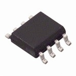
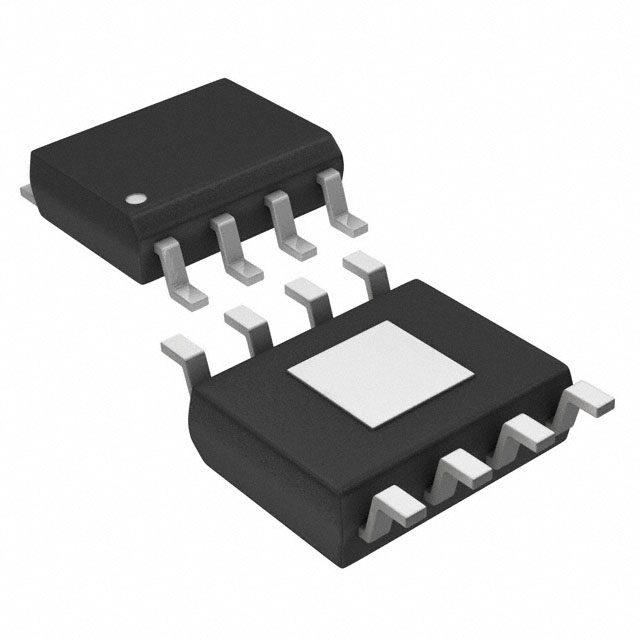
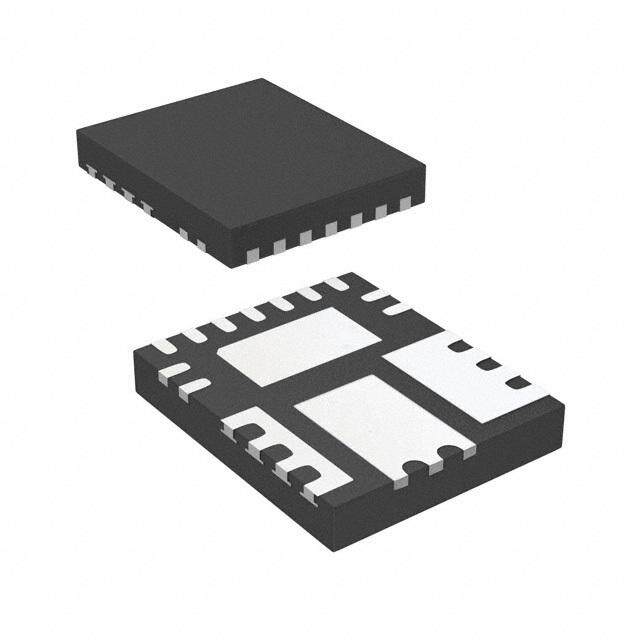
| 产品图片 |
|
| rohs | 符合RoHS无铅 / 符合限制有害物质指令(RoHS)规范要求 |
| 产品系列 | 电源管理 IC,稳压器—开关式稳压器,Analog Devices ADP2303ARDZ-5.0-R7- |
| 数据手册 | |
| 产品型号 | ADP2303ARDZ-5.0-R7 |
| PWM类型 | 电流模式 |
| 产品种类 | 稳压器—开关式稳压器 |
| 供应商器件封装 | 8-SOIC-EP |
| 其它名称 | ADP2303ARDZ-5.0-R7CT |
| 包装 | 剪切带 (CT) |
| 同步整流器 | 无 |
| 商标 | Analog Devices |
| 安装类型 | 表面贴装 |
| 安装风格 | SMD/SMT |
| 宽度 | 3.9 mm |
| 封装 | Reel |
| 封装/外壳 | 8-SOIC(0.154",3.90mm 宽)裸焊盘 |
| 封装/箱体 | SOIC-8 |
| 工作温度 | -40°C ~ 125°C |
| 工厂包装数量 | 1000 |
| 开关频率 | 700 kHz |
| 拓扑结构 | Buck |
| 最大工作温度 | + 125 C |
| 最大输入电压 | 20 V |
| 最小工作温度 | - 40 C |
| 最小输入电压 | 3 V |
| 标准包装 | 1 |
| 电压-输入 | 3 V ~ 20 V |
| 电压-输出 | 5V |
| 电流-输出 | 3A |
| 电源电流 | 720 uA |
| 类型 | 降压(降压) |
| 系列 | ADP2303 |
| 视频文件 | http://www.digikey.cn/classic/video.aspx?PlayerID=1364138032001&width=640&height=505&videoID=2245193149001 |
| 输出数 | 1 |
| 输出电压 | Adj |
| 输出电流 | 3 A |
| 输出端数量 | 1 Output |
| 输出类型 | 固定 |
| 频率-开关 | 700kHz |


- 商务部:美国ITC正式对集成电路等产品启动337调查
- 曝三星4nm工艺存在良率问题 高通将骁龙8 Gen1或转产台积电
- 太阳诱电将投资9.5亿元在常州建新厂生产MLCC 预计2023年完工
- 英特尔发布欧洲新工厂建设计划 深化IDM 2.0 战略
- 台积电先进制程称霸业界 有大客户加持明年业绩稳了
- 达到5530亿美元!SIA预计今年全球半导体销售额将创下新高
- 英特尔拟将自动驾驶子公司Mobileye上市 估值或超500亿美元
- 三星加码芯片和SET,合并消费电子和移动部门,撤换高东真等 CEO
- 三星电子宣布重大人事变动 还合并消费电子和移动部门
- 海关总署:前11个月进口集成电路产品价值2.52万亿元 增长14.8%


PDF Datasheet 数据手册内容提取
2 A/3 A, 20 V, 700 kHz, Nonsynchronous Step-Down Regulators Data Sheet ADP2302/ADP2303 FEATURES TYPICAL APPLICATIONS CIRCUIT Wide input voltage range: 3.0 V to 20 V VIN VIN BST Maximum load current ADP2302/ 2 A for ADP2302 ADP2303 3 A for ADP2303 VOUT PGOOD SW ±1.5% output accuracy over temperature Output voltage down to 0.8 V ON 700 kHz switching frequency OFF EN FB CAuurtroemnta-tmico PdFeM c/oPnWtrMol m arocdheit ecture GND 08833-001 Precision enable pin with hysteresis Figure 1. Typical Application Circuit Integrated high-side MOSFET Integrated bootstrap diode Internal compensation and soft start 100 Power-good output Undervoltage lockout (UVLO) 90 Overcurrent protection (OCP) Thermal shutdown (TSD) %) 80 8-lead SOIC package with exposed paddle Y ( Supported by ADIsimPower™ design tool ENC 70 CI APPLICATIONS FI F E Intermediate power rail conversion 60 DC-to-DC point of load applications Communications and networking 50 VOUT = 3.3V Industrial and instrumentation INDUCTOR: VLF10040T-4R7N5R4 VOUT = 5.0V DIODE: SSB43L Healthcare and medical 40 Consumer 0 0.5 1O.0UTPUT C1U.5RRENT (2A.)0 2.5 3.0 08833-002 Figure 2. ADP2303 Efficiency vs. Output Current at VIN = 12 V GENERAL DESCRIPTION The ADP2302/ADP2303 are fixed frequency, current-mode The ADP2302/ADP2303 have integrated soft start circuitry to control, step-down, dc-to-dc regulators with an integrated prevent a large inrush current at power-up. The power-good power MOSFET. The ADP2302/ADP2303 can run from an signal can be used to sequence devices that have an enable input. input voltage of 3.0 V to 20 V, which makes them suitable for a The precision enable threshold voltage allows the part to be wide range of applications. The output voltage of the ADP2302/ easily sequenced from other input/output supplies. Other key ADP2303 can be down to 0.8 V for the adjustable version, while features include undervoltage lockout (UVLO), overvoltage the fixed output version is available in preset output voltage protection (OVP), thermal shutdown (TSD), and overcurrent options of 5.0 V, 3.3 V, and 2.5 V. The 700 kHz operating protection (OCP). frequency allows small inductor and ceramic capacitors to be The ADP2302/ADP2303 devices are available in the 8-lead, used, providing a compact solution. Current mode control SOIC package with exposed paddle and are rated for the −40oC provides fast and stable line and load transient performance. to +125oC junction temperature range. Rev. A Information furnished by Analog Devices is believed to be accurate and reliable. However, no responsibility is assumed by Analog Devices for its use, nor for any infringements of patents or other One Technology Way, P.O. Box 9106, Norwood, MA 02062-9106, U.S.A. rights of third parties that may result from its use. Specifications subject to change without notice. No license is granted by implication or otherwise under any patent or patent rights of Analog Devices. Tel: 781.329.4700 www.analog.com Trademarks and registered trademarks are the property of their respective owners. Fax: 781.461.3113 ©2010–2012 Analog Devices, Inc. All rights reserved.
ADP2302/ADP2303 Data Sheet TABLE OF CONTENTS Features .............................................................................................. 1 Overvoltage Protection (OVP) ................................................. 15 Applications ....................................................................................... 1 Power Good ................................................................................ 15 Typical Applications Circuit ............................................................ 1 Control Loop ............................................................................... 15 General Description ......................................................................... 1 Applications Information .............................................................. 16 Revision History ............................................................................... 2 ADIsimPower Design Tool ....................................................... 16 Specifications ..................................................................................... 3 Programming Output Voltage .................................................. 16 Absolute Maximum Ratings ............................................................ 4 Voltage Conversion Limitations ............................................... 16 Thermal Resistance ...................................................................... 4 Low Input Voltage Considerations .......................................... 17 ESD Caution .................................................................................. 4 Programming the Precision Enable ......................................... 17 Pin Configuration and Function Descriptions ............................. 5 Inductor ....................................................................................... 17 Typical Performance Characteristics ............................................. 6 Catch Diode ................................................................................ 18 Functional Block Diagram ............................................................ 13 Input Capacitor ........................................................................... 19 Theory of Operation ...................................................................... 14 Output Capacitor........................................................................ 19 Basic Operation .......................................................................... 14 Thermal Consideration ............................................................. 19 PWM Mode ................................................................................. 14 Design Example .............................................................................. 20 Power Saving Mode .................................................................... 14 Catch Diode Selection ............................................................... 20 Bootstrap Circuitry .................................................................... 14 Inductor Selection ...................................................................... 20 Precision Enable ......................................................................... 14 Output Capacitor Selection....................................................... 20 Integrated Soft Start ................................................................... 14 Resistive Voltage Divider Selection .......................................... 20 Current Limit .............................................................................. 14 Circuit Board Layout Recommendations ................................... 22 Short-Circuit Protection ............................................................ 14 Typical Application Circuits ......................................................... 23 Undervoltage Lockout (UVLO) ............................................... 15 Outline Dimensions ....................................................................... 26 Thermal Shutdown (TSD) ......................................................... 15 Ordering Guide .......................................................................... 26 REVISION HISTORY 6/12—Rev. 0 to Rev. A Change to Features Section ............................................................. 1 Added ADIsimPower Design Tool Section ................................. 16 Change to Voltage Conversion Limitations Section .................. 16 Updated Outline Dimensions ....................................................... 26 Changes to Ordering Guide .......................................................... 26 7/10—Revision 0: Initial Version Rev. A | Page 2 of 28
Data Sheet ADP2302/ADP2303 SPECIFICATIONS V = 3.3 V, T = −40°C to +125°C for minimum/maximum specifications, and T = 25°C for typical specifications, unless otherwise noted. IN J A Table 1. Parameters Symbol Test Conditions Min Typ Max Unit VIN Voltage Range V 3.0 20 V IN Supply Current I No switching, V = 12 V 720 950 μA VIN IN Shutdown Current I V = 0 V, V = 12 V 24 45 μA SHDN EN IN Undervoltage Lockout Threshold UVLO V rising 2.7 2.9 V IN V falling 2.2 2.4 V IN FB Regulation Voltage V ADP230xARDZ (adjustable) 0.788 0.8 0.812 V FB ADP230xARDZ-2.5 2.463 2.5 2.538 V ADP230xARDZ-3.3 3.25 3.3 3.35 V ADP230xARDZ-5.0 4.925 5.0 5.075 V Bias Current I ADP230xARDZ (adjustable) 0.01 0.1 μA FB SW On Resistance1 V − V = 5 V, I = 200 mA 80 120 160 mΩ BST SW SW Peak Current Limit ADP2302, V − V = 5 V 2.7 3.5 4.4 A BST SW ADP2303, V − V = 5 V 4.6 5.5 6.4 A BST SW Leakage Current V = V = 0 V, V = 12 V 0.1 5 μA EN SW IN Minimum On Time 126 170 ns Minimum Off Time 210 280 ns OSCILLATOR FREQUENCY f 595 700 805 kHz SW SOFT START TIME 2048 Clock cycles EN Input Threshold V 1.12 1.2 1.28 V EN Input Hysteresis 100 mV Pull-Down Current 1.2 μA BOOTSTRAP VOLTAGE V V = 12 V 4.7 5.0 5.3 V BOOT IN PGOOD PGOOD Rising Threshold 82.5 87.5 92.5 % PGOOD Hysteresis 2.5 % PGOOD Deglitch Time2 32 Clock cycles PGOOD Output Low Voltage 150 300 mV PGOOD Leakage Current V = 5 V 0.1 1 μA PGOOD THERMAL SHUTDOWN Threshold Rising temperature 150 °C Hysteresis 15 °C 1 Pin-to-Pin measurements. 2 Guaranteed by design. Rev. A | Page 3 of 28
ADP2302/ADP2303 Data Sheet ABSOLUTE MAXIMUM RATINGS THERMAL RESISTANCE Table 2. Parameter MAX Rating θ is specified for the worst-case conditions, that is, a device JA VIN, EN, PGOOD −0.3 V to +24 V soldered in a circuit board for surface-mount packages. SW −1.0 V to +24 V Table 3. Thermal Resistance1 BST to SW −0.6 V to +6 V Package Type θ Unit FB, NC −0.3 V to +6 V JA 8-Lead SOIC_N_EP 58.5 °C/W Operating Junction Temperature Range −40°C to +125°C Storage Temperature Range −65°C to +150°C 1 JA is measured using natural convection on JEDEC 4-layer board. Soldering Conditions JEDEC J-STD-020 ESD CAUTION Stresses above those listed under Absolute Maximum Ratings may cause permanent damage to the device. This is a stress rating only; functional operation of the device at these or any other conditions above those indicated in the operational section of this specification is not implied. Exposure to absolute maximum rating conditions for extended periods may affect device reliability. Absolute maximum ratings apply individually only, not in combination. Unless otherwise specified, all voltages are referenced to GND. Rev. A | Page 4 of 28
Data Sheet ADP2302/ADP2303 PIN CONFIGURATION AND FUNCTION DESCRIPTIONS BST 1 ADP2302 8 SW VIN 2 ADP2303 7 GND EN 3 TOP VIEW 6 NC PGOOD 4 (Not to Scale) 5 FB NOTES 1. NC = NO CONNECT. 2 . TTTOHHEEA ENICX E PFXOOTRSEE RTDNHAPEARLD MG ASRLHO ODUIUNSLDSD IPP BALETAI NOSEON L.UDNEDREERDNEATH 08833-003 Figure 3. Pin Configuration (Top View) Table 4. Pin Function Descriptions Pin No. Mnemonic Description 1 BST Bootstrap Supply for the High-Side MOSFET Driver. A 0.1 μF capacitor is connected between SW and BST to provide a floating driver voltage for the power switch. 2 VIN Power Input. Connect to the input power source with a ceramic bypass capacitor to GND directly from this pin. 3 EN Output Enable. Pull this pin high to enable the output. Pull this pin low to disable the output. This pin can also be used as a programmable UVLO input. This pin has an internal 1.2 μA pull-down current to GND. 4 PGOOD Power-Good Open-Drain Output. 5 FB Feedback Voltage Sense Input. For the adjustable version, connect this pin to a resistive divider from V . For OUT the fixed output version, connect this pin to V directly. OUT 6 NC Used for internal testing. Connect to GND or leave this pin floating to ensure proper operation. 7 GND Ground. Connect this pin to the ground plane. 8 SW Switch Node Output. Connect an inductor to V and a catch diode to GND from this pin. OUT 9 (EPAD) Exposed Pad The exposed pad should be soldered to an external ground plane underneath the IC for thermal dissipation. Rev. A | Page 5 of 28
ADP2302/ADP2303 Data Sheet TYPICAL PERFORMANCE CHARACTERISTICS V = 3.3 V, T = 25°C, unless otherwise noted. IN A 100 100 90 90 %) 80 %) 80 Y ( Y ( C C CIEN 70 VOUT = 2.5V CIEN 70 VOUT = 1.5V EFFI 60 VVOOUUTT == 35..30VV EFFI 60 VVVOOOUUUTTT === 213...583VVV VOUT = 5.0V 50 50 INDUCTOR: VLF10040T-6R8N4R5 INDUCTOR: VLF10040T-4R7N5R4 DIODE: SSB43L DIODE: SSB43L 40 40 0 0.5 1O.0UTPUT C1U.5RRENT (2A.0) 2.5 3.0 08833-004 0 0.5 1O.0UTPUT C1U.5RRENT (2A.0) 2.5 3.0 08833-007 Figure 4. ADP2303 Efficiency, VIN = 18 V Figure 7. ADP2303 Efficiency, VIN = 12 V 100 100 90 90 %) 80 %) 80 EFFICIENCY ( 6700 VVVOOOUUUTTT === 111...852VVV EFFICIENCY ( 6700 VVVOOOUUUTTT === 235...530VVV VOUT = 2.5V 50 INDUCTOR: VLF10040T-2R2N7R1 50 INDUCTOR: VLF10040T-6R8N4R5 DIODE: SSB43L DIODE: SSB43L 400 0.5 1O.0UTPUT C1U.5RRENT (2A.0) 2.5 3.0 08833-005 400 0.5 OUTPUT C1U.0RRENT (A) 1.5 2.0 08833-008 Figure 5. ADP2303 Efficiency, VIN = 5 V Figure 8. ADP2302 Efficiency, VIN = 18 V 100 100 90 90 80 80 %) %) Y ( Y ( C C EN 70 EN 70 EFFICI 60 VVVVVOOOOOUUUUUTTTTT ===== 21135.....58530VVVVV EFFICI 60 VVVVOOOOUUUUTTTT ==== 1112....8525VVVV 50 50 INDUCTOR: VLF10040T-6R8N4R5 INDUCTOR: VLF10040T-3R3N6R2 DIODE: SSB43L DIODE: SSB43L 400 0.5 OUTPUT C1U.0RRENT (A) 1.5 2.0 08833-006 400 0.5 OUTPUT C1U.0RRENT (A) 1.5 2.0 08833-009 Figure 6. ADP2302 Efficiency, VIN = 12 V Figure 9. ADP2302 Efficiency, VIN = 5 V Rev. A | Page 6 of 28
Data Sheet ADP2302/ADP2303 0.20 0.20 0.15 0.15 0.10 0.10 %) %) ON ( 0.05 ON ( 0.05 GULATI 0 GULATI 0 NE RE–0.05 AD RE–0.05 LI–0.10 LO–0.10 –0.15 –0.15 –0.205 8 11 VIN (V)14 17 20 08833-010 –0.200 0.5 OUTPUT C1U.0RRENT (A) 1.5 2.0 08833-013 Figure 10. ADP2302 Line Regulation, VOUT = 3.3 V, IOUT = 2 A Figure 13. ADP2302 Load Regulation, VOUT = 3.3V, VIN = 12 V 0.20 0.20 0.15 0.15 0.10 0.10 %) %) ON ( 0.05 ON ( 0.05 ATI ATI UL 0 UL 0 G G E E E R–0.05 D R –0.05 N A LI O –0.10 L –0.10 –0.15 –0.15 –0.205 8 11 VIN (V)14 17 20 08833-011 –0.200 0.5 1O.0UTPUT C1U.5RRENT (2A.)0 2.5 3.0 08833-014 Figure 11. ADP2303 Line Regulation, VOUT = 3.3 V , IOUT = 3 A Figure 14. ADP2303 Load Regulation, VOUT = 3.3 V, VIN = 12 V 50 900 45 850 40 A) A) 800 RENT (μ 3305 RENT (μ 750 R R CU 25 CU 700 OWN 20 CENT 650 D S SHUT 1105 TJ = –40°C QUIE 600 TTJJ == +–4205°°CC 5 TTJJ == ++2152°5C°C 550 TJ = +125°C 0 500 2 4 6 8 10VIN (V1)2 14 16 18 20 08833-012 2 4 6 8 10VIN (V1)2 14 16 18 20 08833-015 Figure 12. Shutdown Current vs. VIN Figure 15. Quiescent Current vs. VIN Rev. A | Page 7 of 28
ADP2302/ADP2303 Data Sheet 810 812 790 810 770 808 750 mV) 806 kHz) 730 GE ( 804 CY ( 710 LTA 802 N O 800 UE 690 K V Q C 798 FRE 670 DBA 796 650 FEE 794 630 792 610 790 590 788 –40 –20 0 T2E0MPER4A0TURE6 (0°C) 80 100 120 08833-016 –40 –20 0 T2E0MPER4A0TURE6 (0°C) 80 100 120 08833-019 Figure 16. Frequency vs. Temperature Figure 19. 0.8 V Feedback Voltage vs. Temperature 4.4 6.4 4.2 6.2 4.0 6.0 A) A) MIT ( 3.8 MIT ( 5.8 LI LI T 3.6 T 5.6 N N E E RR 3.4 RR 5.4 U U C C K 3.2 K 5.2 A A E E P 3.0 P 5.0 2.8 4.8 2.6 4.6 –40 –20 0 T2E0MPER4A0TURE6 (0°C) 80 100 120 08833-017 –40 –20 0 T2E0MPER4A0TURE6 (0°C) 80 100 120 08833-020 Figure 17. ADP2302 Current-Limit Threshold vs. Temperature, VBST − VSW = 5 V Figure 20. ADP2303 Current-Limit Threshold vs. Temperature, VBST − VSW = 5 V 2.9 1.30 2.8 1.25 V) RISING D (V) 2.7 RISING OLD ( 1.20 O THRESHOL 22..56 BLE THRESH 11..1105 FALLING L A UV 2.4 EN FALLING 1.05 2.3 2.2–40 –20 0 T2E0MPER4A0TURE6 (0°C) 80 100 120 08833-018 1.00–40 –20 0 T2E0MPER4A0TURE6 (0°C) 80 100 120 08833-021 Figure 18. UVLO Threshold vs. Temperature Figure 21. Enable Threshold vs. Temperature Rev. A | Page 8 of 28
Data Sheet ADP2302/ADP2303 270 150 265 145 260 140 255 ME (ns) 224550 ME (ns) 113305 M OFF TI 223450 M ON TI 125 MU 230 MU 120 MINI 225 MINI 115 220 110 215 105 210 205 100 –40 –20 0 T2E0MPER4A0TURE6 (0°C) 80 100 120 08833-022 –40 –20 0 T2E0MPER4A0TURE6 (0°C) 80 100 120 08833-025 Figure 22. Minimum Off Time vs. Temperature Figure 25. Minimum On Time vs. Temperature 180 VOUT (AC) 170 1 160 Ω) 150 m R ( 140 IL TO 130 S SI 120 E R SW ET 110 4 OSF 100 VGS = 3V M 90 VGS = 4V 80 VGS = 5V 2 70 60–40 –20 0 T2E0MPER4A0TURE6 (0°C) 80 100 120 08833-023 CH1 5.00mV BW CCHH24 52..0000VA Ω MT 1 .3000.µ00s% A CH2 7.50V 08833-026 Figure 23. MOSFET RDSON vs. Temperature (Pin-to-Pin Measurement) Figure 26. Continuous Conduction Mode (CCM), VOUT = 3.3 V, VIN = 12 V VOUT (AC) 1 VOUT (AC) IL 1 4 IL 4 SW SW 2 2 CH1 5.00mV BW CCHH24 52..0000VA Ω MT 1 .3000.µ00s% A CH2 7.50V 08833-024 CH1 50.00mV BW CCHH24 52..0000VA Ω MT 2 0300µ.0s0% A CH2 7.50V 08833-027 Figure 24. Discontinuous Conduction Mode (DCM), VOUT = 3.3 V, VIN = 12 V Figure 27. Power Saving Mode, VOUT = 3.3 V, VIN = 12 V Rev. A | Page 9 of 28
ADP2302/ADP2303 Data Sheet VOUT VOUT 1 IL 1 IL 4 4 EN EN SW SW 3 3 2 2 CCHH13 120.0.00VV BBWW CCHH24 120.0.00VA Ω MT 1 .2000.m20s% A CH3 6.20V 08833-028 CCHH13 120.0.00VV BBWW CCHH42 21.00.00AV Ω MT 1 .2000.m20s% A CH3 3.60V 08833-031 Figure 28. Soft Start Without Load, VOUT = 3.3 V, VIN = 12 V Figure 31. Soft Start with Full Load, VOUT = 3.3 V, VIN = 12 V VOUT (AC) VOUT (AC) 1 1 IO IO 4 4 CH1 500mV BW CH4 2.00A Ω MT 2 0200µ.0s0% A CH4 1.20A 08833-029 CH1 200mV BW CH4 2.00A Ω MT 2 0200µ.0s0% A CH4 1.88A 08833-032 Figure 29. ADP2303 Load Transient, 0.5 A to 3.0 A, VOUT = 5.0 V, VIN = 12 V, Figure 32. ADP2303 Load Transient, 0.5 A to 3.0 A, VOUT = 3.3 V, VIN = 12 V, L = 4.7 μH, COUT = 47 μF L = 4.7 μH, COUT = 2 × 47 μF VOUT (AC) VOUT (AC) 1 1 IO IO 4 4 CH1 200mV BW CH4 1.00A Ω MT 2 0200µ.0s0% A CH4 1.20A 08833-030 CH1 200mV BW CH4 1.00A Ω MT 2 0200µ.0s0% A CH4 1.20A 08833-033 Figure 30. ADP2302 Load Transient, 0.5 A to 2.0 A, VOUT = 5.0 V, VIN = 12 V, Figure 33. ADP2302 Load Transient, 0.5 A to 2.0 A, VOUT = 3.3 V, VIN = 12 V, L = 6.8 μH, COUT = 2 × 22 μF L = 6.8 μH, COUT = 2 × 22 μF Rev. A | Page 10 of 28
Data Sheet ADP2302/ADP2303 VOUT VOUT 1 1 IL IL SW 4 4 SW 2 2 CH1 1.00mV BW CCHH24 51.00.00VA Ω MT 4 03.00.µ00s% A CH1 1.26V 08833-034 CH1 1.00V BW CCHH24 51.00.00VA Ω MT 4 0300µ.0s0% A CH1 1.26V 08833-037 Figure 34. Output Short, VOUT = 3.3 V, VIN = 12 V, Figure 37. Output Short Recovery, VOUT = 3.3 V, VIN = 12 V, L = 4.7 μH, COUT = 2 × 47 μF L = 4.7 μH, COUT = 2 × 47 μF VOUT VOUT 1 VIN VIN 1 SW SW 3 3 2 2 CCHH31 5 2.000.0VmVBW BW CH2 10.0VBW MT 1 .2030.m40s% A CH3 11.0V 08833-035 CCHH31 52.00.00VmVBW BW CH2 10.0VBW MT 1 .2030.m40s% A CH3 11.0V 08833-038 Figure 35. ADP2303 Line Transient, 7 V to 15 V, VOUT = 3.3 V, IOUT = 3 A, Figure 38. ADP2302 Line Transient, 7 V to 15 V, VOUT = 3.3 V, IOUT = 2 A, L = 4.7 μH, COUT = 2 × 47 μF L = 6.8 μH, COUT = 2 × 22 μF 80 180 80 180 64 144 64 144 48 108 48 108 32 72 32 72 E (dB) 16 36 grees) E (dB) 16 36 grees) UD 0 0 De UD 0 0 De GNIT –16 –36 ASE ( GNIT –16 –36 ASE ( A H A H M –32 –72 P M –32 –72 P –48 –108 –48 –108 –64 CROSS FREQUENCY = 36kHz –144 –64 CROSS FREQUENCY = 42kHz –144 PHASE MARGIN = 60° PHASE MARGIN = 56° –801k 10k FREQUENC1Y0 (0Hkz) 1M –180 08833-036 –801k 10k FREQUENC1Y0 (0Hkz) 1M –180 08833-039 Figure 36. ADP2302 Bode Plot, VOUT = 2.5 V, VIN = 12 V, Figure 39. ADP2302 Bode Plot, VOUT = 3.3 V, VIN = 12 V, L = 4.7 μH, COUT =3 × 22 μF L = 6.8 μH, COUT = 2 × 22 μF Rev. A | Page 11 of 28
ADP2302/ADP2303 Data Sheet 80 180 80 180 64 144 64 144 48 108 48 108 32 72 B) 32 72 s) MAGNITUDE (dB) ––1316260 30––63762 PHASE (Degrees) MAGNITUDE (B/A) (d ––1316260 30––63762 PHASE (B–A) (Degere –48 –108 –48 –108 –64 CROSS FREQUENCY = 32kHz –144 –64 CROSS FREQUENCY = 26kHz –144 PHASE MARGIN = 59° PHASE MARGIN = 65° –801k 10k FREQUENC1Y0 (0Hkz) 1M –180 08833-040 –801k 10k FREQUENC1Y0 (0Hkz) 1M –180 08833-142 Figure 40. ADP2302 Bode Plot, VOUT = 5 V, VIN = 12 V, Figure 42. ADP2303 Bode Plot, VOUT = 2.5 V, VIN = 12 V, L = 6.8 μH, COUT = 2 × 22 μF L = 3.3 μH, COUT = 2 × 47 μF 80 180 80 180 64 144 64 144 48 108 48 108 32 72 B) 32 72 s) E (dB) 16 36 grees) B/A) (d 16 36 Degere MAGNITUD ––13620 0––3762 PHASE (De MAGNITUDE ( ––13620 0––3762 PHASE (B–A) ( –48 –108 –48 –108 –64 CROSS FREQUENCY = 19kHz –144 –64 CROSS FREQUENCY = 28kHz –144 PHASE MARGIN = 59° PHASE MARGIN = 65° –801k 10k FREQUENC1Y0 (0Hkz) 1M –180 08833-041 –801k 10k FREQUENC1Y0 (0Hkz) 1M –180 08833-143 Figure 41. ADP2303 Bode Plot, VOUT = 3.3 V, VIN = 12 V, Figure 43. ADP2303 Bode Plot, VOUT = 5 V, VIN = 12 V, L = 4.7 μH, COUT = 2 × 47 μF L = 4.7 μH, COUT = 47 μF Rev. A | Page 12 of 28
Data Sheet ADP2302/ADP2303 FUNCTIONAL BLOCK DIAGRAM VIN VIN 2 THERMAL SHUTDOWN UVLO SHUTDOWN LOGIC SHUTDOWN IC 1.20V ON OCP CURRENT OFF EN 3 SENSEAMPLIFIER 1.2µA CURRENT REGBUOLOATTOR 1 BST OVP LIMIT 0.880V THRESHOLD R Q S PGOOD 4 VBIAS = 1.1V SW VOUT 8 RAMP CLK 0.680V GENERATOR GENERATOR FREQUENCY FOLDBACK (⅛fSW, ¼fSW, ½fSW,fSW) NC 6 5 gm 0.8V VOLTAGE FB REFERENCE ADP2302/ADP2303 7GND 08833-042 Figure 44. Functional Block Diagram Rev. A | Page 13 of 28
ADP2302/ADP2303 Data Sheet THEORY OF OPERATION Because the output voltage occasionally dips below regulation The ADP2302/ADP2303 are nonsynchronous, step-down, and then recovers, the output voltage ripple in the power saving dc-to-dc regulators, each with an integrated high-side power mode is larger than the ripple in the PWM mode of operation. MOSFET. The high switching frequency and 8-lead SOIC package provide a small, step-down, dc-to-dc regulator BOOTSTRAP CIRCUITRY solution. The ADP2302/ADP2303 each have an integrated boot regulator, The ADP2302/ADP2303 can operate with an input voltage from which requires that a 0.1 μF ceramic capacitor (X5R or X7R) be 3.0 V to 20 V while regulating an output voltage down to 0.8 V. placed between the BST and SW pins to provide the gate drive voltage for the high-side MOSFET. There is at least a 1.2 V The ADP2302 can provide 2 A maximum continuous output difference between the BST and SW pins to turn on the high-side current, and the ADP2303 can provide 3 A maximum MOSFET. This voltage should not exceed 5.5 V in case the BST continuous output current. pin is supplied with the external voltage source through a diode. BASIC OPERATION The ADP2302/ADP2303 generate a typical 5.0 V bootstrap voltage The ADP2302/ADP2303 use the fixed-frequency, peak current- for the gate drive circuit by differentially sensing and regulating mode PWM control architecture from medium to high loads, the voltage between the BST and SW pins. There is a diode but shift to a pulse-skip mode control scheme at light loads to integrated on the chip that blocks the reverse voltage between the reduce the switching power losses and improve efficiency. When VIN and BST pins when the MOSFET switch is turned on. these devices operate in fixed-frequency PWM mode, output PRECISION ENABLE regulation is achieved by controlling the duty cycle of the integrated MOSFET. While the devices are operating in pulse-skip mode at The ADP2302/ADP2303 provide a precision enable circuit that light loads, the output voltage is controlled in a hysteretic has 1.2 V reference threshold with 100 mV hysteresis. When the manner with higher output ripple. In this mode of operation, the voltage at the EN pin is greater than 1.2 V (typical), the part is regulator periodically stops switching for a few cycles, thus enabled. If the EN voltage falls below 1.1 V (typical), the chip keeping the conversion losses minimal to improve efficiency. is disabled. The precision enable threshold voltage allows the ADP2302/ADP2303 to be easily sequenced from other input/ PWM MODE output supplies. It also can be used as a programmable UVLO In PWM mode, the ADP2302/ADP2303 operate at a fixed input by using a resistive divider. An internal 1.2 μA pull-down frequency, set by an internal oscillator. At the start of each current prevents errors if the EN pin is left floating. oscillator cycle, the MOSFET switch is turned on, providing a INTEGRATED SOFT START positive voltage across the inductor. The inductor current increases until the current-sense signal crosses the peak The ADP2302/ADP2303 have an internal digital soft start inductor current threshold that turns off the MOSFET switch; circuitry to limit the output voltage rise time and reduce this threshold is set by the error amplifier output. During the the inrush current at power up. The soft start time is fixed at MOSFET off time, the inductor current declines through the 2048 clock cycles. external diode until the next oscillator clock pulse comes and a CURRENT LIMIT new cycle starts. The ADP2302/ADP2303 include current-limit protection circuitry POWER SAVING MODE to limit the amount of positive current flowing through the high- To achieve higher efficiency, the ADP2302/ADP2303 smoothly side MOSFET switch. The positive current limit on the power transition to the pulse-skip mode when the output load decreases switch limits the amount of current that can flow from the input below the pulse-skip current threshold. When the output vol- to the output. tage dips below the regulation, the ADP2302/ADP2303 enter SHORT-CIRCUIT PROTECTION PWM mode for a few oscillator cycles until the voltage increases The ADP2302/ADP2303 include frequency foldback to prevent to regulation range. During the idle time between bursts, the output current runaway when there is a hard short on the output. MOSFET switch is turned off, and the output capacitor supplies The switching frequency is reduced when the voltage at the FB pin all the output current. drops below a certain value, which allows more time for the Because the pulse-skip mode comparator monitors the internal inductor current to decline, but increases the ripple current while compensation node, which represents the peak inductor current regulating the peak current. This results in a reduction in average information, the average pulse-skip load current threshold output current and prevents output current runaway. The corre- depends on the input voltage (V ), the output voltage (V ), IN OUT lation between the switching frequency and the FB pin voltage the inductor, and the output capacitor. is shown in Table 5. Rev. A | Page 14 of 28
Data Sheet ADP2302/ADP2303 Table 5. Correlation Between f and V OVERVOLTAGE PROTECTION (OVP) SW FB FB Pin Voltage Switching Frequency The ADP2302/ADP2303 provide an overvoltage protection V ≥ 0.6 V f FB SW feature to protect the system against an output short to a higher 0.4 V < V < 0.6 V 1/2 f FB SW voltage supply. If the feedback voltage is above 0.880 V, the 0.2 V < V ≤ 0.4 V 1/4 f FB SW internal high-side MOSFET is turned off, until the voltage at FB V ≤ 0.2 V 1/8 f FB SW decreases to 0.850 V. At that time, the ADP2302/ADP2303 When a hard short (V ≤ 0.2 V) is removed, a soft start cycle resume normal operation. FB is initiated to regulate the output back to its level during normal POWER GOOD operation, which helps to limit the inrush current and prevent The PGOOD pin is an active high, open-drain output and possible overshoot on the output voltage. requires a resistor to pull it up to a voltage (<20.0 V). A high UNDERVOLTAGE LOCKOUT (UVLO) indicates that the voltage on the FB pin (and therefore the The ADP2302/ADP2303 have fixed, internally set undervoltage output voltage) is above 87.5% of the reference voltage. A low lockout circuitry (UVLO). If the input voltage drops below indicates that the voltage on the FB pin is below 85% of the 2.4 V, the ADP2302/ADP2303 shut down and the MOSFET reference voltage. There is a 32-cycle waiting period after FB is switch turns off. After the voltage rises above 2.7 V, the soft detected as being in or out of bounds. start period is initiated, and the part is enabled. CONTROL LOOP THERMAL SHUTDOWN (TSD) The ADP2302/ADP2303 are internally compensated to minimize If the ADP2302/ADP2303 junction temperature rises above 150C, external component count and cost. In addition, the built-in the thermal shutdown circuit disables the chip. Extreme junction slope compensation helps to prevent subharmonic oscillations temperature can be the result of high current operation, poor when the ADP2302/ADP2303 operate at a duty cycle greater circuit board design, or high ambient temperature. A 15C than or close to 50%. hysteresis is included so that when thermal shutdown occurs, the ADP2302/ADP2303 do not return to operation until the on- chip temperature drops below 135C. When the devices recover from thermal shutdown, a soft start is initiated. Rev. A | Page 15 of 28
ADP2302/ADP2303 Data Sheet APPLICATIONS INFORMATION ADIsimPower DESIGN TOOL for the worst case. By considering the variation of both the switch- ing frequency and the input voltage, the equation for the lower The ADP2302/ADP2303 are supported by the ADIsimPower limit of the output voltage is design tool set. ADIsimPower is a collection of tools that produce V = t × f × (V + V ) − V complete power designs optimized for a specific design goal. OUT(min) MIN-ON SW(max) IN(max) D D The tools enable the user to generate a full schematic and bill of where: materials, and calculate performance in minutes. ADIsimPower V is the maximum input voltage. IN(max) can optimize designs for cost, area, efficiency, and parts count f is the maximum switching frequency for the worst case. SW(max) while taking into consideration the operating conditions and t is the minimum controllable on time. MIN-ON limitations of the IC and all real external components. For V is the diode forward drop. D more information about ADIsimPower design tools, refer to The upper limit of the output voltage is constrained by the mini- www.analog.com/ADIsimPower. The tool set is available from mum controllable off time, which can be as high as 280 ns in this website, and users can request an unpopulated board ADP2302/ADP2303 for the worst case. By considering the through the tool. variation of both the switching frequency and the input voltage, PROGRAMMING OUTPUT VOLTAGE the equation for the upper limit of the output voltage is ADP2302/ADP2303 have an adjustable version where the output V = (1 − t × f ) × (V + V ) − V OUT(max) MIN-OFF SW(max) IN(min) D D voltage is programmed through an external resistive divider, as where: shown in Figure 45. Suggested resistor values for the typical V is the minimum input voltage. IN(min) output voltage setting are listed in Table 6. The output voltages f is the maximum switching frequency for the worst case. SW(max) are calculated using the following equation: V is the diode forward drop. D R tMIN-OFF is the minimum controllable off time. V 0.800V1 TOP OUT RBOT In addition, the bootstrap circuit limits the minimum input voltage for the desired output due to the internal dropout voltage. To where: attain stable operation at light loads and ensure proper startup for V is the output voltage. OUT the prebiased condition, the ADP2302/ADP2303 require the R is the feedback resistor from V to FB. TOP OUT voltage difference between the input voltage and the regulated R is the feedback resistor from FB to GND. BOT output voltage (or between the input voltage and the prebias voltage) to be greater than 2.1 V for the worst case. If the voltage difference is smaller, the bootstrap circuit relies on some minimum ADP2302/ load current to charge the boost capacitor for startup. Figure 46 ADP2303 VOUT shows the typical required minimum input voltage vs. load current RTOP for the 3.3 V output voltage. FB 5.3 RBOT 08833-043 5.1 FOR START UP Figure 45. Programming the Output Voltage Using a Resistive Voltage Divider 4.9 4.7 Table 6. Suggested Values for Resistive Voltage Divider VOUT (V) RTOP (kΩ), ±1% RBOT (kΩ), ±1% V) 4.5 1.2 10 20 V (IN 4.3 1.5 10 11.3 4.1 WHILE IN 1.8 12.7 10.2 OPERATION 2.5 21.5 10.2 3.9 3.3 31.6 10.2 3.7 5.0 52.3 10 3.5 VOLTAGE CONVERSION LIMITATIONS 1 10OUPTUT CURRE10N0T (mA) 1000 08833-146 There are both lower and upper output voltage limitations for a Figure 46. Minimum Input Voltage vs. Load Current given input voltage due to the minimum on time, the minimum Based on three conversion limitations (the minimum on time, off time, and the bootstrap dropout voltage. the minimum off time, and the bootstrap dropout voltage), The lower limit of the output voltage is constrained by the Figure 47 shows the voltage conversion limitations. controllable minimum on time, which can be as high as 170 ns Rev. A | Page 16 of 28
Data Sheet ADP2302/ADP2303 22 VIN 20 VIN MAXIMUM INPUT VOLTAGE 18 ADP2302/ 16 REN1 ADP2303 14 V) EN (N12 VI108 REN2 08833-047 Figure 49. Precision Enable Used as a Programmable UVLO 6 MINIMUM INPUT VOLTAGE The precision enable feature also allows the ADP2302/ADP2303 to 4 be sequenced precisely by using a resistive voltage divider from 20 2 4 6 VOU8T (V) 10 12 14 16 08833-147 another dc-to-dc power supply, as shown in Figure 50. Figure 47. Voltage Conversion Limitations LOW INPUT VOLTAGE CONSIDERATIONS ADP2302/ For low input voltage between 3 V and 5 V, the internal boot ADP2303 regulator cannot provide enough bootstrap voltage due to the ANOTHER REN1 internal dropout voltage. As a result, the increased MOSFET DC/DC EN SUPPLIER abRnoD oSe(OtxsNtt)er rraenpda bul icsamess av tlohl-lets aiaggvena.ai Blla Sebcclaehu olostetak dtyh c edu iarobrdeseno tlfu.r oTtemo m p ara e5xv.i0me nVut m tehx ritsae,tr ainndagdl REN2 08833-048 Figure 50. Precision Enable Used as a Sequencing Control between the BST and SW pins is 6.0 V, the bias voltage should from Another DC-to-DC Power Supply be less than 5.5 V. Figure 48 shows the application diagram for With a 1.2 μA pull-down current on the EN pin, the equation for the external bootstrap circuit. the start-up voltage in Figure 49 and Figure 50 is SCHOTTKY 3.0V ~ 5.0V DIODE 1.2V VIN BST V 1.2μAR 1.2V ADP2302/ 5V BIAS VOLTAGE STARTUP REN2 EN1 ADP2303 where: SW V is the start-up voltage to enable the chip. STARTUP R is the resistor from the dc source to EN. EN1 ON OFF EN FB REN2 is the resistor from EN to GND. GND 08833-046 ITNhDe hUigChT sOwRitc hing frequency of the ADP2302/ADP2303 allows Figure 48. External Bootstrap Circuit for Low Input Voltage Application the use of small inductors. For best performance, use inductor PROGRAMMING THE PRECISION ENABLE values between 1 μH and 15 μH. Generally, the EN pin can connect to the VIN pin so that the The peak-to-peak inductor ripple current is calculated using the device automatically starts up when the input power is applied. following equation: However, the precision enabling feature allows the ADP2302/ ADP2303 to be used as a programmable UVLO by connecting (V V ) V V I IN OUT OUT D a resistive voltage divider to VIN, as shown in Figure 49. This RIPPLE L fsw VIN VD configuration prevents the start-up problems that can occur where: when VIN ramps up slowly in soft start with a relatively high f is the switching frequency. load current. SW L is the inductor value. V is the diode forward drop. D V is the input voltage. IN V is the output voltage. OUT Inductors of smaller values are usually smaller in size but increase the ripple current and the output ripple voltage. As a guideline, the inductor peak-to-peak ripple current is typically set to 30% of the maximum load current for optimal transient Rev. A | Page 17 of 28
ADP2302/ADP2303 Data Sheet response and efficiency. Therefore, the inductor value is calculated CATCH DIODE using the following equation: The catch diode conducts the inductor current during the off V V V V time of the internal MOSFET. The average current of the diode L IN OUT OUT D in normal operation is, therefore, dependent on the duty cycle 0.3ILOAD(max) fsw VIN VD of the regulator as well as the output load current. where I is the maximum load current. LOAD(max) V V Teqhuea itniodnu:c tor peak current is calculated using the following IDIODE(AVG) 1 VOIUNTVDD ILOAD(max) I where VD is the diode forward drop. I I RIPPLE PEAK LOAD(max) 2 The only reason to select a diode with a higher current rating than necessary in normal operation is for the worst-case condi- The minimum current rating of the inductor must be greater tion, in which there is a shorted output. In this case, the diode than the inductor peak current. For ferrite core inductors with a current increases up to the typical peak current limit threshold. quick saturation characteristic, the inductor saturation current Be sure to consult the diode data sheet to ensure that the diode rating should be higher than the switch current limit threshold can operate well within the thermal and electrical limits. to prevent the inductor from reaching its saturation point. Be sure to validate the worst-case condition, in which there is a The reverse breakdown voltage rating of the diode must be higher shorted output, over the intended temperature range. than the highest input voltage and allow an appropriate margin for the ringing that may be present on the SW node. A Schottky Inductor conduction loss is caused by the flow of current diode is recommended for the best efficiency because it has a through internal dc resistance (DCR). Larger sized inductors low forward voltage drop and fast switching speed. Table 7 have smaller DCR of the inductor and, therefore, may reduce provides a list of recommended Schottky diodes. inductor conduction losses. Inductor core loss is related to the core material and the ac flux swing, which are affected by the Table 7. Recommended Schottky Diodes peak-to-peak inductor ripple current. Because the ADP2302/ Vendor Part No. V (V) I (A) RRM AVG ADP2303 are high frequency switching regulators, shielded fer- Vishay SSB43L 30 4 rite core materials are recommended for their low core losses SSA33L 30 3 and low EMI. Some recommended inductors are shown in ON Semiconductor MBRS330T3 30 3 Table 8. Diodes Inc. B330B 30 3 Table 8. Recommended Inductors Vendor Value (μH) Part No. DCR (mΩ) I (A) Dimensions L × W × H (mm) SAT Sumida 2.5 CDRH104RNP-2R5N 7.8 7.5 10.5 × 10.3 × 3.8 3.8 CDRH104RNP-3R8N 9.6 6 10.5 × 10.3 × 3.8 5.2 CDRH104RNP-5R2N 16 5.5 10.5 × 10.3 × 3.8 7 CDRH104RNP-7R0N 20 4.8 10.5 × 10.3 × 3.8 10 CDRH104RNP-100N 26 4.4 10.5 × 10.3 × 3.8 Coilcraft 2.5 MSS1038-252NL 10 7.62 10 × 10.2 × 3.8 3.8 MSS1038-382NL 13 6.5 10 × 10.2 × 3.8 5.2 MSS1038-522NL 22 5.28 10 × 10.2 × 3.8 7 MSS1038-702NL 27 4.74 10 × 10.2 × 3.8 10 MSS1038103NL 35 3.9 10 × 10.2 × 3.8 Toko 2.8 #919AS-2R8M 10.7 8.3 10.3 × 10.3 × 4.5 3.7 #919AS-3R7M 14.2 7 10.3 × 10.3 × 4.5 4.7 #919AS-4R7M 16.2 6.1 10.3 × 10.3 × 4.5 6.4 #919AS-6R4M 22.9 5.2 10.3 × 10.3 × 4.5 10 #919AS-100M 26.5 4.3 10.3 × 10.3 × 4.5 TDK 2.2 VLF10040T-2R2N7R1 7.9 8.2 10 × 9.7 × 4.0 3.3 VLF10040T-3R3N6R2 10.5 6.7 10 × 9.7 × 4.0 4.7 VLF10040T-4R7N5R4 12.7 5.4 10 × 9.7 × 4.0 6.8 VLF10040T-6R8N4R5 19.8 4.6 10 × 9.7 × 4.0 10 VLF10040T-100M3R8 28 3.8 10 × 9.7 × 4.0 Rev. A | Page 18 of 28
Data Sheet ADP2302/ADP2303 INPUT CAPACITOR coefficients. Y5V and Z5U dielectrics are not recommended because of their poor temperature and dc bias characteristics. The input capacitor must be able to support the maximum input operating voltage and the maximum RMS input current. The In general, most applications require a minimum output rms ripple current flowing through the input capacitor is, at capacitor value of 2 × 22 μF. maximum, I /2. Select an input capacitor capable of LOAD(max) Some recommended output capacitors for V ≤ 5.0 V are OUT withstanding the rms ripple current for an application’s maxi- provided in Table 9. mum load current using the following equation: THERMAL CONSIDERATION I I D1D IN(RMS) LOAD(max) ADP2302/ADP2303 have an internal high-side MOSFET and where D is the duty cycle and is equal to its drive circuit. Only a small amount of power dissipates inside the ADP2302/ADP2303 package under typical load conditions, V V D OUT D which reduces thermal constraints. V V IN D However, in applications with maximum loads at high ambient The recommended input capacitance is ceramic with X5R or X7R temperature and high duty cycle, the heat dissipated in the dielectrics due to its low ESR and small temperature coefficients. package may cause the junction temperature of the die to A capacitance of 10 μF should be adequate for most applications. exceed the maximum junction temperature of 125°C. If the To minimize supply noise, place the input capacitor as close as junction temperature exceeds 150°C, the regulator goes into possible to the VIN pin of the ADP2302/ADP2303. thermal shutdown and recovers when the junction temperature drops below 135°C. OUTPUT CAPACITOR The junction temperature of the die is the sum of the ambient The output capacitor selection affects both the output voltage ripple temperature and the temperature rise of the package due to and the loop dynamics of the regulator. The ADP2302/ADP2303 power dissipation, as indicated in the following equation: are designed to operate with small ceramic capacitors that have low ESR and equivalent series inductance (ESL) and are, therefore, T = T + T J A R easily able to meet stringent output voltage ripple specifications. where: When the regulator operates in continuous conduction mode, T is the junction temperature. J the overall output voltage ripple is the sum of the voltage spike T is the ambient temperature. A caused by the output capacitor equivalent series resistance T is the rising temperature of the package due to power R (ESR) plus the voltage ripple caused by the charging and dissipation. discharging of the output capacitor The rising temperature of the package is directly proportional 1 to the power dissipation in the package. The proportionality VRIPPLE IRIPPLE8fswCOUT ESRCOUT cjuonncsttiaonnt ofof rt hthei sd iree ltaot itohnes ahmipb iise ntht et etmhepremraatlu rrees,i satsa nshcoe wfrno min tthhee Capacitors with lower ESR are preferable to guarantee low following equation: output voltage ripple, as shown in the following equation: T = θ × P R JA D V ESR RIPPLE where: Cout I T is the rising temperature of the package. RIPPLE R θ is the thermal resistance from the junction of the die to the Ceramic capacitors are manufactured with a variety of dielec- JA ambient temperature of the package. trics, each with different behavior over temperature and applied P is the power dissipation in the package. voltage. X5R or X7R dielectrics are recommended for best D performance, due to their low ESR and small temperature Table 9. Recommended Capacitors for V ≤ 5.0 V OUT Vendor Value Part No. Dimensions L × W × H (mm) Murata 22 μF, 6.3 V, X5R GRM31CR60J226KE19 3.2 × 2.5 × 2.0 47 μF, 6.3 V, X5R GRM32ER60J476ME20 3.2 × 2.5 × 2.0 TDK 22 μF, 6.3 V, X5R C3216X5R0J226MB 3.2 × 1.6 × 0.85 33 μF, 6.3 V, X5R C3216X5R0J336MB 3.2 × 1.6 × 1.3 47 μF, 6.3 V, X5R C3225X5R0J476MB 3.2 × 2.5 × 2.5 Rev. A | Page 19 of 28
ADP2302/ADP2303 Data Sheet DESIGN EXAMPLE This section provides the procedures to select the external compo- The inductor peak current is calculated using the following nents, based on the example specifications listed in Table 10. equation: The schematic for this design example is shown in Figure 51. I Because the output current is 3 A, the ADP2303 is chosen for I I RIPPLE PEAK LOAD(max) 2 this application. where: Table 10. Step-Down DC-to-DC Regulator Requirements I = 3 A. LOAD(max) Additional ΔI = 0.7 A. RIPPLE Parameter Specification Requirements The calculated peak current for the inductor is 3.4 A. Therefore, Input Voltage, V 12.0 V ± 10% None IN in this application, select VLF10040T-4R7N5R4 as the inductor. Output Voltage, V 3.3 V, 3 A, 1% V ripple None OUT OUT at full load condition OUTPUT CAPACITOR SELECTION Programmable V start-up voltage None IN Select the output capacitor based on the minimum output UVLO Voltage approximately 7.8 V voltage ripple requirement, according to the following equation: PGOOD Not used None 1 CATCH DIODE SELECTION V I ESR Select the catch diode. A Schottky diode is recommended for best RIPPLE RIPPLE 8fswCOUT COUT efficiency because it has a low forward voltage drop and faster where: switching speed. The average current of the catch diode in ΔIRIPPLE = 0.7 A. normal operation, with a typical Schottky diode forward fSW = 700 kHz. voltage, can be calculated using the following equation: ΔVRIPPLE = 33 mV (1% of output voltage). V V If ESR of the ceramic capacitor is 3 mΩ, then COUT = 4 μF. I 1 OUT D I DIODE(AVG) VIN VD LOAD(max) Because the output capacitor is one of two external components that control the loop stability and according to the recommended where: external components in Table 11, choose two 47 μF capacitor V = 3.3 V. OUT with a 6.3 V voltage rating in this application. V = 12 V. IN RESISTIVE VOLTAGE DIVIDER SELECTION I = 3 A. LOAD(max) V = 0.4 V. The output feedback resistive voltage divider is D Therefore, IDIODE(AVG) = 2.1 A. R V 0.800V1 TOP In this case, selecting a SSB43L, 4.0 A, 30 V surface-mount OUT RBOT Schottky diode results in more reliable operation. For the 3.3 V output voltage, choose R = 31.6 kΩ and TOP INDUCTOR SELECTION R = 10.2 kΩ as the feedback resistive voltage divider BOT Select the inductor by using the following equation: according to the recommended values in Table 11. V V V V The resistive voltage divider for the programmable VIN start-up L IN OUT OUT D voltage is 0.3ILOAD(max)fsw VIN VD 1.2V where: V 1.2μAR 1.2V VOUT = 3.3 V. STARTUP REN2 EN1 V = 12 V. IN If V = 7.8 V, choose R = 10.2 kΩ, and then calculate STARTUP EN2 I = 3 A. LOAD(max) R , which, in this case, is 56 kΩ. EN1 V = 0.4 V. D f = 700 kHz. SW This results in L = 4.12 μH. The closest standard value is 4.7 μH; therefore, ΔI = 0.7 A. RIPPLE Rev. A | Page 20 of 28
Data Sheet ADP2302/ADP2303 VIN= 12V VIN BST 120C5µIVFN RP1G00OkOΩD ADP2303 C0.B1SµTF VOUT= 3.3V REN1 3A 56kΩ SW 1% PGOOD D 4.7LµH COUT1 COUT2 RTOP SSB43L 47µF 47µF 31.6kΩ 6.3V 6.3V 1% EN 10R.2EkNΩ2 GND FB RBOT 1% 110%.2kΩ 08833-049 Figure 51. Schematic for the Design Example Table 11. Recommended External Components for Typical Applications at 2 A/3 A Output Load Part Number V (V) V (V) I (A) L (μH) C R (kΩ), ±1% R (kΩ), ±1% IN OUT LOAD(max) OUT TOP BOT ADP2302 18 3.3 2 6.8 2 × 22 μF 31.6 10.2 18 5.0 2 10 2 × 22 μF 52.3 10 12 1.5 2 4.7 2 × 47 μF 10 11.3 12 1.8 2 4.7 3 × 22 μF 12.7 10.2 12 2.5 2 4.7 3 × 22 μF 21.5 10.2 12 3.3 2 6.8 2 × 22 μF 31.6 10.2 12 5.0 2 6.8 2 × 22 μF 52.3 10 5 1.5 2 3.3 2 × 47 μF 10 11.3 5 1.8 2 3.3 2 × 47 μF 12.7 10.2 5 2.5 2 3.3 2 × 22 μF 21.5 10.2 ADP2303 18 3.3 3 4.7 2 × 47 μF 31.6 10.2 18 5.0 3 6.8 47 μF 52.3 10 12 1.5 3 2.5 3 × 47 μF 10 11.3 12 1.8 3 3.3 3 × 47 μF 12.7 10.2 12 2.5 3 3.3 2 × 47 μF 21.5 10.2 12 3.3 3 4.7 2 × 47 μF 31.6 10.2 12 5.0 3 4.7 47 μF 52.3 10 5 1.5 3 2.2 3 × 47 μF 10 11.3 5 1.8 3 2.2 3 × 47 μF 12.7 10.2 5 2.5 3 2.2 3 × 47 μF 21.5 10.2 Rev. A | Page 21 of 28
ADP2302/ADP2303 Data Sheet CIRCUIT BOARD LAYOUT RECOMMENDATIONS Good circuit board layout is essential to obtaining the best Minimize the length of the FB trace connecting the top of performance for ADP2302/ADP2303. Poor layout can affect the the feedback resistive voltage divider to the output. In regulation and stability, as well as the electromagnetic interface addition, keep these traces away from the high current (EMI) and electromagnetic compatibility (EMC) performance. traces and the switch node to avoid noise pickup. A PCB layout example is shown in Figure 53. Refer to the following guidelines for a good PCB layout: VIN BST ADP2302/ Place the input capacitor, the inductor, catch diode, output ADP2303 capacitor, and bootstrap capacitor close to the IC using PGOOD SW short traces. Ensure that the high current loop traces are as short and EN FB wide as possible. The high current path is shown Figure 52. Mto aimximpriozvee t hthee srimzea ol fd gisrsoipuantdio mn.e tal on the component side GND 08833-050 Figure 52. Typical Application Circuit with High Current Lines Shown in Blue Use a ground plane with several vias connecting to the component side ground to further reduce noise on sensitive circuit nodes. VOUT INDUCTOR OUTPUT CAPACITORS DIODE GND BST CAP INPUT BST 1 EXPOSED 8 SW CAPACITOR PAD VIN 2 7 GND VIN EN 3 6 NC PGOOD 4 5 FB 08833-051 Figure 53. Recommended Layout for ADP2302/ADP2303 Rev. A | Page 22 of 28
Data Sheet ADP2302/ADP2303 TYPICAL APPLICATION CIRCUITS VIN= 12V VIN BST 10CµIFN ADP2302ARDZ CBST 25V 0.1µF VOUT= 1.5V 2A EN SW RP1G00OkOΩD DB330B 4.7LµH C47OµUFT1 C47OµUFT2 R10TkOΩP 6.3V 6.3V 1% PGOOD FB GND RBOT 111%.3kΩ 08833-052 Figure 54. ADP2302 Typical Application, VIN = 12 V, VOUT = 1.5 V, 2 A VIN= 12V VIN BST 10CµIFN ADP2302ARDZ CBST 25V 0.1µF VOUT= 1.8V 2A EN SW RP1G00OkOΩD DB330B 4.7LµH C22OµUFT1 C22OµUFT2 C22OµUFT3 1R2T.O7PkΩ 6.3V 6.3V 6.3V 1% PGOOD FB GND RBOT 110%.2kΩ 08833-053 Figure 55. ADP2302 Typical Application, VIN = 12 V, VOUT = 1.8 V, 2 A VIN= 12V VIN BST 120C5µIVFN ADP2302ARDZ-2.5 C0.B1SµTF VOUT= 2.5V 2A EN SW L D 4.7µH COUT1 COUT2 COUT3 B330B 22µF 22µF 22µF 6.3V 6.3V 6.3V PGOOD FB GND 08833-054 Figure 56. ADP2302 Typical Application, VIN = 12 V, VOUT = 2.5 V, 2 A VIN VIN BST 120C5µIVFN RP1G00OkOΩD ADP2302ARDZ-3.3 C0.B1SµTF VOUT= 3.3V REN1 2A 56kΩ SW 1% PGOOD D 6.8LµH COUT1 COUT2 B330B 22µF 22µF 6.3V 6.3V EN REN2 FB 10.21k%Ω GND 08833-055 Figure 57. ADP2302 Typical Application, VIN = 12 V, VOUT = 3.3 V, 2 A, with Programmable 7.8 V UVLO Rev. A | Page 23 of 28
ADP2302/ADP2303 Data Sheet VIN= 12V VIN BST 10CµIFN ADP2302ARDZ-5.0 CBST 25V 0.1µF VOUT= 5.0V 2A EN SW RP1G00OkOΩD DB330B 6.8LµH C22OµUFT1 C22OµUFT2 16V 16V PGOOD FB GND 08833-056 Figure 58. ADP2302 Typical Application, VIN = 12 V, VOUT = 5 V, 2 A VIN= 12V VIN BST 10CµIFN ADP2303ARDZ CBST 25V 0.1µF VOUT= 1.5V 3A EN SW RP1G00OkOΩD DSSB43L2.5LµH C47OµUFT1 C47OµUFT2 C47OµUFT3 1R0TkOΩP 6.3V 6.3V 6.3V 1% PGOOD FB GND RBOT 111%.3kΩ 08833-057 Figure 59. ADP2303 Typical Application, VIN = 12 V, VOUT = 1.5 V, 3 A VIN= 12V VIN BST 10CµIFN ADP2303ARDZ CBST 25V 0.1µF VOUT= 1.8V 3A EN SW RP1G00OkOΩD DSSB43L3.3LµH 4C7OµUFT1 4C7OµUFT2 C47OµUFT3 R12T.O7PkΩ 6.3V 6.3V 6.3V 1% PGOOD FB GND RBOT 110%.2kΩ 08833-058 Figure 60. ADP2303 Typical Application, VIN = 12 V, VOUT = 1.8 V, 3 A VIN= 12V VIN BST 10CµIFN ADP2303ARDZ CBST 25V 0.1µF VOUT= 2.5V 3A EN SW RP1G00OkOΩD DSSB43L3.3LµH 4C7OµUFT1 4C7OµUFT2 R21T.O5PkΩ 6.3V 6.3V 1% PGOOD FB GND RBOT 110%.2kΩ 08833-059 Figure 61. ADP2303 Typical Application, VIN = 12 V, VOUT = 2.5 V, 3 A Rev. A | Page 24 of 28
Data Sheet ADP2302/ADP2303 VIN= 12V VIN BST 10CµIFN ADP2303ARDZ-5.0 CBST 25V 0.1µF VOUT= 5V 3A EN SW RP1G00OkOΩD DSSB43L4.7LµH C47OµUFT1 6.3V PGOOD FB GND 08833-060 Figure 62. ADP2303 Typical Application, VIN = 12 V, VOUT = 5 V, 3 A VIN= 5V VIN BST 10CµIFN ADP2302ARDZ CBST 25V 0.1µF VOUT= 1.2V 2A EN SW RP1G00OkOΩD DB330B 3.3LµH 4C7OµUFT1 4C7OµUFT2 1R0TkOΩP 6.3V 6.3V 1% PGOOD FB GND RBOT 210%kΩ 08833-061 Figure 63. ADP2302 Typical Application, VIN = 5V, VOUT = 1.2 V, 2 A Rev. A | Page 25 of 28
ADP2302/ADP2303 Data Sheet OUTLINE DIMENSIONS 5.00 4.90 2.29 4.80 0.356 8 5 6.20 4.00 6.00 3.90 5.80 2.29 3.80 0.457 1 4 FOR PROPER CONNECTION OF 1.27 BSC BOTTOM VIEW THE EXPOSED PAD, REFER TO 3.81 REF THE PIN CONFIGURATION AND FUNCTION DESCRIPTIONS TOP VIEW SECTION OF THIS DATA SHEET. 1.75 1.65 0.50 45° 1.35 1.25 0.25 0.25 0.17 0.10 MAX SEATING PLANE 0.51 0.05 NOM 8° 1.04 REF 0.31 COPL0A.1N0ARITY 0° 10..2470 COMPLIANTTO JEDEC STANDARDS MS-012-AA 06-02-2011-B Figure 64. 8-Lead Standard Small Outline Package, with Exposed Pad [SOIC_N_EP] Narrow Body (RD-8-1) Dimensions shown in millimeters ORDERING GUIDE Model1 Output Voltage Temperature Range Package Description Package Option ADP2302ARDZ Adjustable −40°C to +125°C 8-Lead SOIC_N_EP, Tube RD-8-1 ADP2302ARDZ-2.5 2.5 V −40°C to +125°C 8-Lead SOIC_N_EP, Tube RD-8-1 ADP2302ARDZ-3.3 3.3 V −40°C to +125°C 8-Lead SOIC_N_EP, Tube RD-8-1 ADP2302ARDZ-5.0 5.0 V −40°C to +125°C 8-Lead SOIC_N_EP, Tube RD-8-1 ADP2302ARDZ-R7 Adjustable −40°C to +125°C 8-Lead SOIC_N_EP, 7” Tape and Reel RD-8-1 ADP2302ARDZ-2.5-R7 2.5 V −40°C to +125°C 8-Lead SOIC_N_EP, 7” Tape and Reel RD-8-1 ADP2302ARDZ-3.3-R7 3.3 V −40°C to +125°C 8-Lead SOIC_N_EP, 7” Tape and Reel RD-8-1 ADP2302ARDZ-5.0-R7 5.0 V −40°C to +125°C 8-Lead SOIC_N_EP, 7” Tape and Reel RD-8-1 ADP2302-EVALZ Evaluation Board ADP2303ARDZ Adjustable −40°C to +125°C 8-Lead SOIC_N_EP, Tube RD-8-1 ADP2303ARDZ-2.5 2.5 V −40°C to +125°C 8-Lead SOIC_N_EP, Tube RD-8-1 ADP2303ARDZ-3.3 3.3 V −40°C to +125°C 8-Lead SOIC_N_EP, Tube RD-8-1 ADP2303ARDZ-5.0 5.0 V −40°C to +125°C 8-Lead SOIC_N_EP, Tube RD-8-1 ADP2303ARDZ-R7 Adjustable −40°C to +125°C 8-Lead SOIC_N_EP, 7” Tape and Reel RD-8-1 ADP2303ARDZ-2.5-R7 2.5 V −40°C to +125°C 8-Lead SOIC_N_EP, 7” Tape and Reel RD-8-1 ADP2303ARDZ-3.3-R7 3.3 V −40°C to +125°C 8-Lead SOIC_N_EP, 7” Tape and Reel RD-8-1 ADP2303ARDZ-5.0-R7 5.0 V −40°C to +125°C 8-Lead SOIC_N_EP, 7” Tape and Reel RD-8-1 ADP2303-EVALZ Evaluation Board 1 Z = RoHS Compliant Part. Rev. A | Page 26 of 28
Data Sheet ADP2302/ADP2303 NOTES Rev. A | Page 27 of 28
ADP2302/ADP2303 Data Sheet NOTES ©2010–2012 Analog Devices, Inc. All rights reserved. Trademarks and registered trademarks are the property of their respective owners. D08833-0-6/12(A) Rev. A | Page 28 of 28