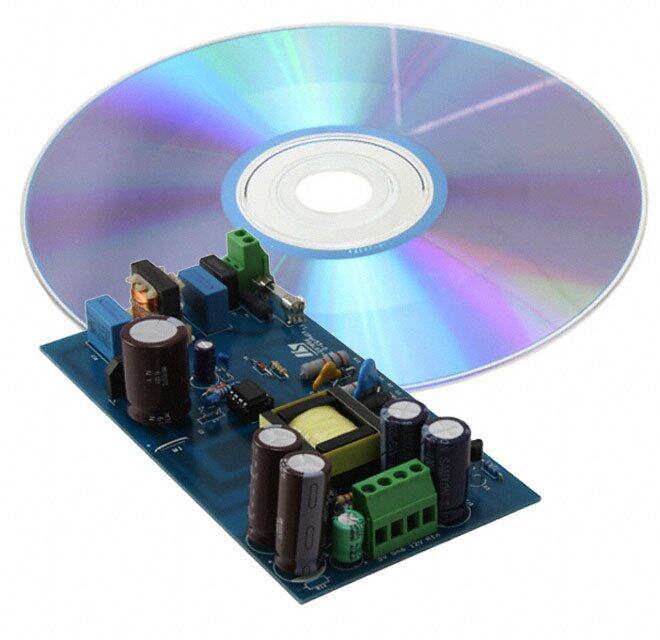
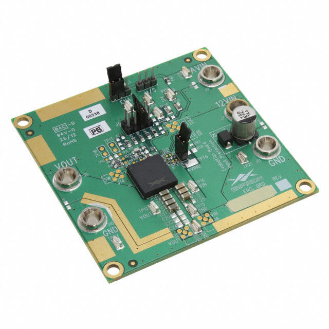
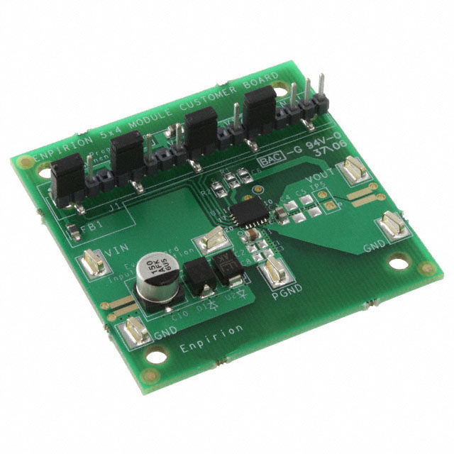
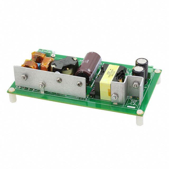
ICGOO在线商城 > 开发板,套件,编程器 > 评估板 - DC/DC 与 AC/DC(离线)SMPS > ADP2300-EVALZ
- 型号: ADP2300-EVALZ
- 制造商: Analog
- 库位|库存: xxxx|xxxx
- 要求:
| 数量阶梯 | 香港交货 | 国内含税 |
| +xxxx | $xxxx | ¥xxxx |
查看当月历史价格
查看今年历史价格
ADP2300-EVALZ产品简介:
ICGOO电子元器件商城为您提供ADP2300-EVALZ由Analog设计生产,在icgoo商城现货销售,并且可以通过原厂、代理商等渠道进行代购。 ADP2300-EVALZ价格参考。AnalogADP2300-EVALZ封装/规格:评估板 - DC/DC 与 AC/DC(离线)SMPS, ADP2300 - DC/DC, Step Down 1, Non-Isolated Outputs Evaluation Board。您可以下载ADP2300-EVALZ参考资料、Datasheet数据手册功能说明书,资料中有ADP2300-EVALZ 详细功能的应用电路图电压和使用方法及教程。
| 参数 | 数值 |
| 产品目录 | 编程器,开发系统 |
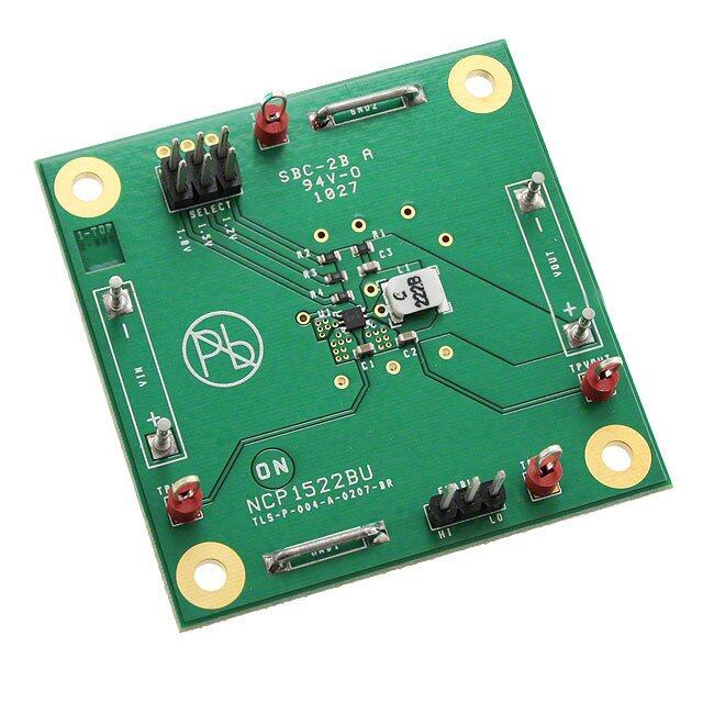
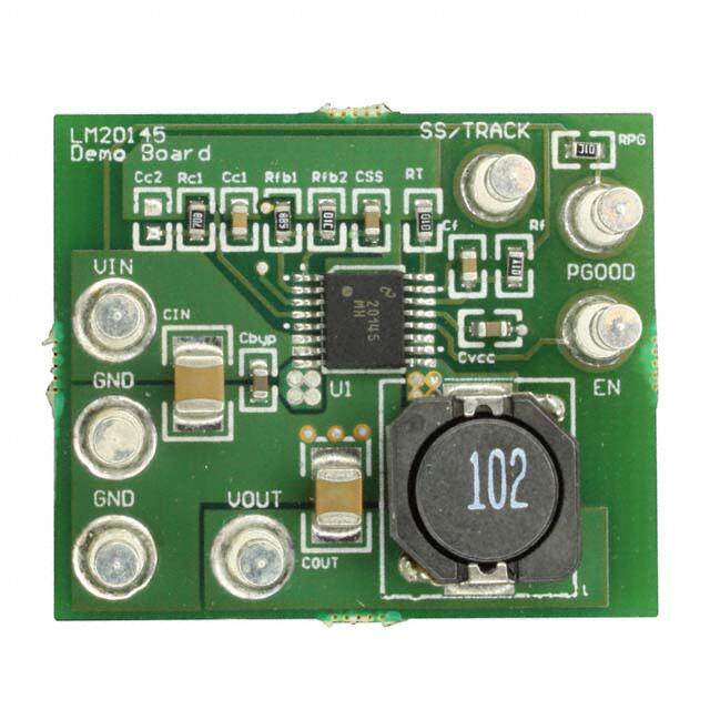
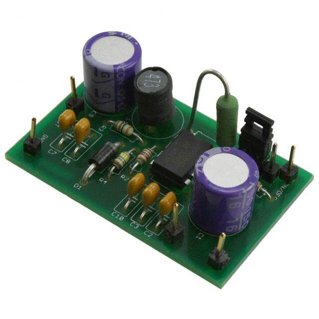
| 描述 | BOARD EVALUATION FOR ADP2300 |
| 产品分类 | |
| 品牌 | Analog Devices Inc |
| 数据手册 | |
| 产品图片 |
|
| 产品型号 | ADP2300-EVALZ |
| rohs | 无铅 / 符合限制有害物质指令(RoHS)规范要求 |
| 产品系列 | - |
| 主要用途 | DC/DC,步降 |
| 使用的IC/零件 | ADP2300 |
| 其它名称 | ADP2300EVALZ |
| 功率-输出 | - |
| 参考设计库 | http://designs.digikey.com/library/4294959904/4294959903/1050 |
| 所含物品 | 板 |
| 板类型 | 完全填充 |
| 标准包装 | 1 |
| 电压-输入 | 3 V ~ 20 V |
| 电压-输出 | 3.3V |
| 电流-输出 | 1.2A |
| 稳压器拓扑 | 降压 |
| 输出和类型 | 1,非隔离 |
| 频率-开关 | 700kHz |


PDF Datasheet 数据手册内容提取
Evaluation Board User Guide UG-179 One Technology Way • P.O. Box 9106 • Norwood, MA 02062-9106, U.S.A. • Tel: 781.329.4700 • Fax: 781.461.3113 • www.analog.com Evaluation Board for the 1.2 A, 20 V Nonsynchronous Step-Down Regulators FEATURES GENERAL DESCRIPTION 1.2 A maximum load current The ADP2300/ADP2301 are compact, constant-frequency, current- ±2% output accuracy over temperature range mode, step-down dc-to-dc regulators with an integrated power Wide input voltage range: 3.0 V to 20 V MOSFET. The ADP2300/ADP2301 evaluation boards are complete Output voltage from 0.8 V to 0.85 × VIN solutions that allow the user to evaluate the performance of the 700 kHz (ADP2300) or 1.4 MHz (ADP2301) switching regulators. There are two frequency options available: the ADP2300 frequency options runs at 700 kHz, and the ADP2301 runs at 1.4 MHz. These options Automatic PFM/PWM mode switching allow the user to make design decisions based on the trade-off Precision enable pin with hysteresis between efficiency and the size of the total solution. Integrated high-side MOSFET The ADP2300/ADP2301 provide accurate (±2%) output regulation Integrated bootstrap diode for load currents up to 1.2 A. Current-mode control provides fast ADIsimPower™ online design tool and stable line and load transient performance. The precision, Available in ultrasmall, 6-lead TSOT package EN pin, threshold voltage allows the ADP2300/ADP2301 to be sequenced from other input/output supplies. The EN pin can also be used as a programmable UVLO input by using a resistive divider. DEMONSTRATION BOARD 09232-001 Figure 1. PLEASE SEE THE LAST PAGE FOR AN IMPORTANT WARNING AND LEGAL TERMS AND CONDITIONS. Rev. 0 | Page 1 of 12
UG-179 Evaluation Board User Guide TABLE OF CONTENTS Features .............................................................................................. 1 Input and Output Voltmeter Connections.................................3 General Description ......................................................................... 1 Power On the Evaluation Board ..................................................3 Demonstration Board ...................................................................... 1 Measuring Evaluation Board Performance ...................................3 Revision History ............................................................................... 2 Typical Performance Characteristics ..............................................5 Using the Evaluation Board ............................................................. 3 Demonstration Board Schematics and Bill of Materials ..............7 Jumper Setting .............................................................................. 3 ADP2300 Schematic and Bill of Materials .................................7 Input Power Source Connection ................................................ 3 ADP2301 Schematic and Bill of Materials .................................8 Output Load Connection ............................................................ 3 Demonstration Board Layout ..........................................................9 REVISION HISTORY 8/10—Revision 0: Initial Version Rev. 0 | Page 2 of 12
Evaluation Board User Guide UG-179 USING THE EVALUATION BOARD The ADP2300/ADP2301 evaluation boards are fully assembled Connect the input voltage measuring the voltmeter’s positive and tested. Before applying power to the evaluation boards, follow terminal (+) to the input capacitor (C2) positive terminal and the the procedures in this section. negative (−) terminal to the input capacitor (C2) negative terminal. JUMPER SETTING Connect the output voltage measuring the voltmeter’s positive (+) Jumper J5 enables the part. Connect a jumper between Position 1 terminal to the output capacitor (C3 or C4) positive terminal and Position 2 to enable the part. Connect a jumper between and the negative (−) terminal to the output capacitor (C3 or C4) Position 2 and Position 3 to disable the part. Leave Jumper J5 negative terminal. open to obtain an approximately 7.8 V V start-up voltage. IN POWER ON THE EVALUATION BOARD Table 1. Jumper J5 (EN) Setting When the power source and load are connected to the ADP2300/ State Function ADP2301 evaluation board, they can be powered up for operation. High Enable the part If the input power source voltage goes higher than 7.8 V with Low Disable the part Jumper J5 open, the output voltage goes up to 3.3 V. Open Program the V start-up voltage to be about 7.8 V IN MEASURING EVALUATION BOARD PERFORMANCE INPUT POWER SOURCE CONNECTION Measuring the Switching Waveform Before connecting the power source to the ADP2300/ADP2301 To observe the switching waveform with an oscilloscope, place evaluation board, make sure that the evaluation board is turned off. the oscilloscope probe tip at the end of inductor connected to If the input power source includes a current meter, use that the SW pin with the probe ground at GND. Set the scope to dc, meter to monitor the input current. Connect the positive terminal 5 V/division, and 1 μs/division time base. The switching waveform of the power source to the VIN terminal (J1) on the evaluation should alternate between 0 V and approximately the input voltage. board, and the negative terminal of the power source to the Measuring Load Regulation GND terminal (J3) of the board. If the power source does not Load regulation should be tested by increasing the load current include a current meter, connect a current meter in series with at the output and measuring the output voltage across the output the input source voltage. Connect the positive terminal of the capacitor (C3 or C4). power source to the current meter’s positive lead (+), the negative terminal of the power source to the GND terminal (J3) on the Measuring Line Regulation evaluation board, and the negative lead (−) of the current meter Vary the input voltage and measure the output voltage at a fixed to the VIN terminal (J1) on the board. output current. The input voltage can be measured across the OUTPUT LOAD CONNECTION input capacitor (C2), and the output voltage can be measured across the output capacitor (C3 or C4). Make sure that the board is turned off before connecting the load. If the load includes a current meter, or if the current is not Measuring Efficiency measured, connect the load directly to the demonstration board The efficiency, η, is measured by comparing the input power with the positive (+) load connection to the VOUT terminal (J2) with the output power. and negative (−) load connection to the GND terminal (J4). If a V ×I current meter is used, connect it in series with the load; connect η= OUT OUT V ×I the positive (+) current meter terminal to the evaluation board IN IN VOUT terminal (J2), the negative (−) current meter terminal to Measuring Inductor Current the positive (+) load terminal, and the negative (−) load terminal to The inductor current is measured by removing one end of the the evaluation board GND terminal (J4). inductor from the pad on the board and using a wire connected INPUT AND OUTPUT VOLTMETER CONNECTIONS between the pad and the inductor. Then a current probe is used to measure the inductor current. Measure the input and output voltages with voltmeters. Make sure that the voltmeters are connected to the appropriate test point on the board. If the voltmeters are not connected to the right test point, the measured voltages will be incorrect due to the voltage drop across the leads and/or connections between the board, the power source, and/or the load. Rev. 0 | Page 3 of 12
UG-179 Evaluation Board User Guide Measuring Output Voltage Ripple Varying the Output voltage To observe the output voltage ripple, place an oscilloscope probe The ADP2300/ADP2301 demonstration board output is preset across the output capacitor (C3 or C4) with the probe ground to 3.3 V; however, the output voltage can be adjusted to other lead at the negative (−) capacitor terminal and the probe tip at output voltages using the following equation: the positive (+) capacitor terminal. Set the oscilloscope to ac, ⎛ R ⎞ 1 mV/division, and 1 μs/division time base, 20 MHz bandwidth. V =0.800V×⎜1+ 2⎟ OUT ⎜ R ⎟ The standard oscilloscope probe has a long wire ground clip. ⎝ 4⎠ For high frequency measurements, this ground clip picks up high frequency noise and injects it into the measured output ripple. Make sure to keep the ground lengths on the oscilloscope probe as short as possible to get a clean voltage ripple measurement. Rev. 0 | Page 4 of 12
Evaluation Board User Guide UG-179 TYPICAL PERFORMANCE CHARACTERISTICS 100 0.20 fSW = 1.4MHz 0.15 fSW = 700kHz 90 0.10 %) Y (%) 80 TION ( 0.05 C A EN 70 UL 0 EFFICI 60 AD REG–0.05 O L–0.10 50 VOUT = 5.0V –0.15 INDUCTOR: LPS6225-472MLC VOUT = 3.3V DIODE: B230A VOUT = 2.5V 40 –0.20 0 0.2 0.4 IOU0T.6 (A) 0.8 1.0 1.2 09232-072 0 0.2 0.4 IOU0T.6 (A) 0.8 1.0 1.2 09232-067 Figure 2. Efficiency Curve, VIN = 12 V, fSW = 1.4 MHz Figure 5. Load Regulation, VOUT = 3.3 V, VIN = 12 V 100 INDUCTOR: LPS6225-103MLC DIODE: B230A 90 VOUT 1 IL 80 %) Y ( C N 70 CIE SW FFI 4 E 60 VOUT = 5.0V 50 VOUT = 3.3V VOUT = 2.5V 2 VOUT = 1.8V VOUT = 1.2V 400 Figure0 .32. Efficien0.c4y CurIvOeU0, T.V6 (INA )= 12 V0.,8 fSW = 7001. 0kHz 1.2 09232-073 FigCuHr1e 56m. SVteaBdWy SCCtHHa24t e 55 aV0t0 mHAeaBΩvWy B LWoMa4d00, nfSsW = 1.4A M CHHz,2 I O U T 7 =.4 1V A 09232-024 0.20 fSW = 1.4MHz 0.15 fSW = 700kHz VOUT 1 0.10 %) N ( 0.05 O TI A UL 0 4 IL G E E R–0.05 N LI –0.10 SW –0.15 2 –0.205Figure 4. L8ine Regulat1i1onV, IVNO (UVT) = 134.3 V, IOUT = 15700 mA 20 09232-068 FigCuHre1 7 2. 0SmteVadyB SWtaCCtHHe24 a 5t2 V0L0igmhAt BΩLWo BaWMd1, 0fSµWs = 1.4 MHAz, ICOHUT2 = 4 08 VmA09232-025 Rev. 0 | Page 5 of 12
UG-179 Evaluation Board User Guide VOUT VOUT 1 IL 1 4 EN VIN SW SW 3 3 2 2 CCHH13 110VVBBWW CCHH24 1500V0mAΩBBWW M100µs A CH3 8V 09232-026 CCHH13 55mVV BW CH2 10V BW M1ms A CH3 11.4V 09232-061 Figure 8. Soft Start with 1 A Resistance Load, fSW = 1.4 MHz Figure 11. ADP2301 Line Transient, 7 V to 15 V, VOUT = 3.3 V, IOUT = 1.2 A, fSW = 1.4 MHz 100 200 80 160 VOUT 60 120 1 B) 40 80 s) IOUT B/A] (d 20 40 Degree UDE [ 0 0 B/A] ( GNIT–20 –40 ASE [ 4 SW MA–40 –80 PH –60 –120 2 –80 CROSS FREQUENCY: 80kHz –160 PHASE MARGIN: 68° CH1 50mV BW CCHH42 15000VmA ΩBBWW M100µs A CH4 630mA 09232-058 –1001k 10k FREQUENC1Y0 (0Hkz) 1M –200 09232-063 Figure 9. ADP2301 Load Transient, 0.2 A to 1.0 A, VOUT = 3.3 V, VIN = 12 V Figure 12. ADP2301 Bode Plot, VOUT = 3.3 V, VIN = 12 V (fSW = 1.4 MHz, L = 4.7 μH, COUT = 22 μF) (fSW = 1.4 MHz, L = 4.7 μH, COUT = 22 μF) 100 200 80 160 VOUT 60 120 1 B) 40 80 s) IOUT B/A] (d 20 40 Degree UDE [ 0 0 B/A] ( GNIT–20 –40 ASE [ 4 SW MA–40 –80 PH –60 –120 2 –80 CROSS FREQUENCY: 47kHz –160 PHASE MARGIN: 77° CH1 100mV BWCCHH24 1500V0mA ΩBBWW M100µs A CH4 630mA 09232-060 –1001k 10k FREQU1ENC1Y0 0(Hkz) 1M –200 09232-065 Figure 10. ADP2300 Load Transient, 0.2 A to 1.0 A, VOUT = 3.3 V, VIN = 12 V Figure 13. ADP2300 Bode Plot, VOUT = 3.3 V, VIN = 12 V (fSW = 700 kHz, L = 10 μH, COUT = 22 μF) (fSW = 700 kHz, L = 10 μH, COUT = 22 μF) Rev. 0 | Page 6 of 12
Evaluation Board User Guide UG-179 DEMONSTRATION BOARD SCHEMATICS AND BILL OF MATERIALS ADP2300 SCHEMATIC AND BILL OF MATERIALS L1 J2 10µH VOUT C4 C3 D1 C1 J4 NC 22µF B230A 0.1µF U1 GND 1 BST SW 6 J1 2 GND VIN 5 VIN R2 31.6kΩ C2 3 FB EN 4 10µF J3 10.2kRΩ4 ADP2300 R101kΩ 1 J5 GND (700kHz) 2 3 R3 1.8kΩ EN 09232-014 Figure 14. ADP2300 Demonstration Board Schematic Table 2. ADP2300 Demonstration Board Bill of Materials Qty Reference Designator Description Manufacturer Part Number 1 C1 Capacitor, 0.1 μF, 25 V, 0603, X7R Murata GRM188R71E104KA01 1 C2 Capacitor, 10 μF, 25 V, 1206, X5R Murata GRM31CR61E106KA12 1 C3 Capacitor, 22 μF, 6.3 V, 1206, X5R Murata GRM31CR60J226KE19 1 C4 No assembly N/A1 N/A1 1 D1 Schottky diode, 2 A, 30 V, SMA Diodes, Inc. B230A 4 J1, J2, J3, J4 Header, 1 × 2, 0.1 pitch Harwin M20-9990246 1 J5 Header, 1 × 3, 0.1 pitch Harwin M20-9990346 1 L1 Shielded power inductor, 10 μH, 2.1 A Coilcraft, Inc. LPS6225-103MLC 1 R1 Resistor, 10 kΩ, 1%, 0603 Vishay CRCW060310K0FKEA 1 R2 Resistor, 31.6 kΩ, 1%, 0603 Vishay CRCW060331K6FKEA 1 R3 Resistor, 1.8 kΩ, 1%, 0603 Vishay CRCW06031K80FKEA 1 R4 Resistor, 10.2 kΩ, 1%, 0603 Vishay CRCW060310K2FKEA 1 U1 1.2 A, 20 V, 700 kHz nonsynchronous step-down Analog Devices, Inc. ADP2300 switching regulator 1 N/A is not applicable. Rev. 0 | Page 7 of 12
UG-179 Evaluation Board User Guide ADP2301 SCHEMATIC AND BILL OF MATERIALS L1 J2 4.7µH VOUT C4 C3 D1 C1 J4 NC 22µF B230A 0.1µF U1 GND 1 BST SW 6 J1 2 GND VIN 5 VIN R2 31.6kΩ C2 3 FB EN 4 10µF J3 10.2kRΩ4 ADP2301 R101kΩ 1 J5 GND (1.4MHz) 2 3 R3 1.8kΩ EN 09232-015 Figure 15. ADP2301 Demonstration Board Schematic Table 3. ADP2301 Demonstration Board Bill of Materials Qty Reference Designator Description Manufacturer Part Number 1 C1 Capacitor, 0.1 μF, 25 V, 0603, X7R Murata GRM188R71E104KA01 1 C2 Capacitor, 10 μF, 25 V, 1206, X5R Murata GRM31CR61E106KA12 1 C3 Capacitor, 22 μF, 6.3 V, 1206, X5R Murata GRM31CR60J226KE19 1 C4 No assembly N/A1 N/A1 1 D1 Schottky diode, 2 A, 30 V, SMA Diodes, Inc. B230A 4 J1, J2, J3, J4 Header, 1 × 2, 0.1 pitch Harwin M20-9990246 1 J5 Header, 1 × 3, 0.1 pitch Harwin M20-9990346 1 L1 Shielded power inductor, 4.7 μH, 3.0 A Coilcraft, Inc. LPS6225-472MLC 1 R1 Resistor, 10 kΩ, 1%, 0603 Vishay CRCW060310K0FKEA 1 R2 Resistor, 31.6 kΩ, 1%, 0603 Vishay CRCW060331K6FKEA 1 R3 Resistor, 1.8 kΩ, 1%, 0603 Vishay CRCW06031K80FKEA 1 R4 Resistor, 10.2 kΩ, 1%, 0603 Vishay CRCW060310K2FKEA 1 U1 1.2 A, 20 V, 1.4 MHz nonsynchronous step-down Analog Devices, Inc. ADP2301 switching regulator 1 N/A is not applicable. Rev. 0 | Page 8 of 12
Evaluation Board User Guide UG-179 DEMONSTRATION BOARD LAYOUT 09232-016 09232-018 Figure 16. Demonstration Board, Top Layer Figure 18. Demonstration Board, Second Layer 09232-017 09232-019 Figure 17. Demonstration Board, Third Layer Figure 19. Demonstration Board, Bottom Layer Rev. 0 | Page 9 of 12
UG-179 Evaluation Board User Guide NOTES Rev. 0 | Page 10 of 12
Evaluation Board User Guide UG-179 NOTES Rev. 0 | Page 11 of 12
UG-179 Evaluation Board User Guide NOTES ESD Caution ESD (electrostatic discharge) sensitive device. Charged devices and circuit boards can discharge without detection. Although this product features patented or proprietary protection circuitry, damage may occur on devices subjected to high energy ESD. Therefore, proper ESD precautions should be taken to avoid performance degradation or loss of functionality. Legal Terms and Conditions By using the evaluation board discussed herein (together with any tools, components documentation or support materials, the “Evaluation Board”), you are agreeing to be bound by the terms and conditions set forth below (“Agreement”) unless you have purchased the Evaluation Board, in which case the Analog Devices Standard Terms and Conditions of Sale shall govern. Do not use the Evaluation Board until you have read and agreed to the Agreement. Your use of the Evaluation Board shall signify your acceptance of the Agreement. This Agreement is made by and between you (“Customer”) and Analog Devices, Inc. (“ADI”), with its principal place of business at One Technology Way, Norwood, MA 02062, USA. Subject to the terms and conditions of the Agreement, ADI hereby grants to Customer a free, limited, personal, temporary, non-exclusive, non-sublicensable, non-transferable license to use the Evaluation Board FOR EVALUATION PURPOSES ONLY. Customer understands and agrees that the Evaluation Board is provided for the sole and exclusive purpose referenced above, and agrees not to use the Evaluation Board for any other purpose. Furthermore, the license granted is expressly made subject to the following additional limitations: Customer shall not (i) rent, lease, display, sell, transfer, assign, sublicense, or distribute the Evaluation Board; and (ii) permit any Third Party to access the Evaluation Board. As used herein, the term “Third Party” includes any entity other than ADI, Customer, their employees, affiliates and in-house consultants. The Evaluation Board is NOT sold to Customer; all rights not expressly granted herein, including ownership of the Evaluation Board, are reserved by ADI. CONFIDENTIALITY. This Agreement and the Evaluation Board shall all be considered the confidential and proprietary information of ADI. Customer may not disclose or transfer any portion of the Evaluation Board to any other party for any reason. Upon discontinuation of use of the Evaluation Board or termination of this Agreement, Customer agrees to promptly return the Evaluation Board to ADI. ADDITIONAL RESTRICTIONS. Customer may not disassemble, decompile or reverse engineer chips on the Evaluation Board. Customer shall inform ADI of any occurred damages or any modifications or alterations it makes to the Evaluation Board, including but not limited to soldering or any other activity that affects the material content of the Evaluation Board. Modifications to the Evaluation Board must comply with applicable law, including but not limited to the RoHS Directive. TERMINATION. ADI may terminate this Agreement at any time upon giving written notice to Customer. Customer agrees to return to ADI the Evaluation Board at that time. LIMITATION OF LIABILITY. THE EVALUATION BOARD PROVIDED HEREUNDER IS PROVIDED “AS IS” AND ADI MAKES NO WARRANTIES OR REPRESENTATIONS OF ANY KIND WITH RESPECT TO IT. ADI SPECIFICALLY DISCLAIMS ANY REPRESENTATIONS, ENDORSEMENTS, GUARANTEES, OR WARRANTIES, EXPRESS OR IMPLIED, RELATED TO THE EVALUATION BOARD INCLUDING, BUT NOT LIMITED TO, THE IMPLIED WARRANTY OF MERCHANTABILITY, TITLE, FITNESS FOR A PARTICULAR PURPOSE OR NONINFRINGEMENT OF INTELLECTUAL PROPERTY RIGHTS. IN NO EVENT WILL ADI AND ITS LICENSORS BE LIABLE FOR ANY INCIDENTAL, SPECIAL, INDIRECT, OR CONSEQUENTIAL DAMAGES RESULTING FROM CUSTOMER’S POSSESSION OR USE OF THE EVALUATION BOARD, INCLUDING BUT NOT LIMITED TO LOST PROFITS, DELAY COSTS, LABOR COSTS OR LOSS OF GOODWILL. ADI’S TOTAL LIABILITY FROM ANY AND ALL CAUSES SHALL BE LIMITED TO THE AMOUNT OF ONE HUNDRED US DOLLARS ($100.00). EXPORT. Customer agrees that it will not directly or indirectly export the Evaluation Board to another country, and that it will comply with all applicable United States federal laws and regulations relating to exports. GOVERNING LAW. This Agreement shall be governed by and construed in accordance with the substantive laws of the Commonwealth of Massachusetts (excluding conflict of law rules). Any legal action regarding this Agreement will be heard in the state or federal courts having jurisdiction in Suffolk County, Massachusetts, and Customer hereby submits to the personal jurisdiction and venue of such courts. The United Nations Convention on Contracts for the International Sale of Goods shall not apply to this Agreement and is expressly disclaimed. ©2010 Analog Devices, Inc. All rights reserved. Trademarks and registered trademarks are the property of their respective owners. UG09232-0-8/10(0) Rev. 0 | Page 12 of 12

 Datasheet下载

