ICGOO在线商城 > ADP1653ACPZ-R7
- 型号: ADP1653ACPZ-R7
- 制造商: Analog
- 库位|库存: xxxx|xxxx
- 要求:
| 数量阶梯 | 香港交货 | 国内含税 |
| +xxxx | $xxxx | ¥xxxx |
查看当月历史价格
查看今年历史价格
ADP1653ACPZ-R7产品简介:
ICGOO电子元器件商城为您提供ADP1653ACPZ-R7由Analog设计生产,在icgoo商城现货销售,并且可以通过原厂、代理商等渠道进行代购。 提供ADP1653ACPZ-R7价格参考¥12.69-¥13.99以及AnalogADP1653ACPZ-R7封装/规格参数等产品信息。 你可以下载ADP1653ACPZ-R7参考资料、Datasheet数据手册功能说明书, 资料中有ADP1653ACPZ-R7详细功能的应用电路图电压和使用方法及教程。
| 参数 | 数值 |
| 产品目录 | 集成电路 (IC) |
| 描述 | IC LED DRVR PHOTO FLASH 16-LFCSP |
| 产品分类 | |
| 品牌 | Analog Devices Inc |
| 数据手册 | |
| 产品图片 |
|
| 产品型号 | ADP1653ACPZ-R7 |
| PCN其它 | |
| rohs | 无铅 / 符合限制有害物质指令(RoHS)规范要求 |
| 产品系列 | - |
| 产品目录页面 | |
| 供应商器件封装 | 16-LFCSP-VQ (3x3) |
| 其它名称 | ADP1653ACPZ-R7CT |
| 内部驱动器 | 是 |
| 包装 | 剪切带 (CT) |
| 安装类型 | 表面贴装 |
| 封装/外壳 | 16-VFQFN 裸露焊盘,CSP |
| 工作温度 | -40°C ~ 125°C |
| 恒压 | - |
| 恒流 | - |
| 拓扑 | PWM,升压(升压) |
| 标准包装 | 1 |
| 电压-电源 | 3 V ~ 5.5 V |
| 电压-输出 | - |
| 类型-初级 | 闪灯/白光 |
| 类型-次级 | 白色 LED |
| 输出数 | 1 |
| 频率 | 1.2MHz |




- 商务部:美国ITC正式对集成电路等产品启动337调查
- 曝三星4nm工艺存在良率问题 高通将骁龙8 Gen1或转产台积电
- 太阳诱电将投资9.5亿元在常州建新厂生产MLCC 预计2023年完工
- 英特尔发布欧洲新工厂建设计划 深化IDM 2.0 战略
- 台积电先进制程称霸业界 有大客户加持明年业绩稳了
- 达到5530亿美元!SIA预计今年全球半导体销售额将创下新高
- 英特尔拟将自动驾驶子公司Mobileye上市 估值或超500亿美元
- 三星加码芯片和SET,合并消费电子和移动部门,撤换高东真等 CEO
- 三星电子宣布重大人事变动 还合并消费电子和移动部门
- 海关总署:前11个月进口集成电路产品价值2.52万亿元 增长14.8%

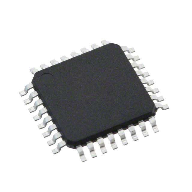
PDF Datasheet 数据手册内容提取
Compact, High Efficiency, High Power, Flash/Torch LED Driver with Dual Interface Data Sheet ADP1653 FEATURES GENERAL DESCRIPTION Small 6.4 mm × 7.2 mm solution The ADP1653 is a very compact, high efficiency, high power, 2.2 μH power inductor camera flash LED driver optimized for cellular phones. The 92% peak efficiency high efficiency and dynamic LED current control of the device Tx masking within 50 μs improve flash brightness and picture quality in dimly lit 2.1 A, 12 V power switch environments. Efficiency peaks at 92% and is higher than Pin-selectable interface: 2-bit logic or I2C charge pump solutions over the Li-Ion battery range. Programmable flash and torch current The device has a dual-mode interface that is configurable to 2-bit Up to 200 mA in torch mode logic or an I2C® interface. The indicator and high power LED Up to 500 mA in flash mode currents are programmable with external resistors or through the Programmable indicator LED current up to 20 mA I2C interface. To maximize overall flash brightness, the ADP1653 Programmable timer register: up to 820 ms flash timeout offers an input to reduce flash LED current in less than 50 μs, 2.75 V to 5.5 V input voltage range referred to as the Tx mask. Tx masking reduces battery stress by Low noise, 1.2 MHz PWM operation scaling back flash LED current during an RF transmission. Safety features Interrupt output pin The ADP1653 solution requires only four external components Fault condition register in I2C mode and fits in a 6.4 mm × 7.2 mm space. The part inte- Short-circuit protection grates multiple safety features such as soft start, flash timeout, Output overvoltage protection output current limit, thermal protection, and overvoltage Thermal overload protection protection. Integrated current limit and soft start The ADP1653 operates over the −40°C to +125°C junction Small 3 mm × 3 mm, 16-lead LFCSP footprint temperature range. APPLICATIONS Camera-enabled cellular phones, smart phones Digital still cameras, camcorders, PDAs TYPICAL OPERATING CIRCUIT PCB LAYOUT INPUT VOLTAGE = 2.75VTO 5.5V LI-ION + GND INPUT CAPACITOR 4.7µF INDUCTOR 2.2µH ON ON L1 C1 OFF OFF UPTO 10.2V SCHOTTKY DIODE 4.7µF 16 15 14 13 STR EN VDD LX D1 OPTIONAL 1 SETT PGND 12 ONE OR 7.2mm TxMASK 2 SETF ADP1653 INT 11 LTEWDOs C2 TO WHITE LEDs 3 CTRL1/SCL INTF 10 OUTPUT CAPACITOR R5 PGND 4 CTRL0/SDA HPLED 9 L = FDSE0312-2R2 CIN = GRM219R61A475K SETI ILED OUT GND D1 = BAT20J COUT = GRM21BR61C475K 5 6 7 8 R4 ADP1653 VDD Figure 1. 06180-001 OPTIONAL (Tx MASK ONLY6).4mm FLREDOsM WHITE 06180-036 Figure 2. Rev. C Document Feedback Information furnished by Analog Devices is believed to be accurate and reliable. However, no responsibility is assumed by Analog Devices for its use, nor for any infringements of patents or other One Technology Way, P.O. Box 9106, Norwood, MA 02062-9106, U.S.A. rights of third parties that may result from its use. Specifications subject to change without notice. No license is granted by implication or otherwise under any patent or patent rights of Analog Devices. Tel: 781.329.4700 ©2007–2017 Analog Devices, Inc. All rights reserved. Trademarks and registered trademarks are the property of their respective owners. Technical Support www.analog.com
ADP1653 Data Sheet TABLE OF CONTENTS Features .............................................................................................. 1 Typical Performance Characteristics ..............................................9 Applications ....................................................................................... 1 Theory of Operation ...................................................................... 13 General Description ......................................................................... 1 White LED Driver ...................................................................... 13 Typical Operating Circuit ................................................................ 1 2-Bit Logic Interface Mode (INTF = 1) ................................... 14 PCB Layout ........................................................................................ 1 I2C Interface Mode (INTF = 0)................................................. 14 Revision History ............................................................................... 2 Turning on the Flash and Watchdog Timer ........................... 15 Specifications ..................................................................................... 3 Safety Features ............................................................................ 16 I2C Timing Specifications ............................................................ 5 Applications Information .............................................................. 17 Absolute Maximum Ratings ............................................................ 6 Flash Current Foldback During Transmit Pulse .................... 17 Thermal Resistance ...................................................................... 6 External Component Selection ................................................ 18 Boundary Condition .................................................................... 6 PCB Layout ................................................................................. 20 ESD Caution .................................................................................. 6 Outline Dimensions ....................................................................... 22 Pin Configuration and Function Descriptions ............................. 7 Ordering Guide .......................................................................... 22 REVISION HISTORY 4/2017—Rev. B to Rev. C Changed CP-16-3 to CP-16-27 .................................... Throughout Changes to Figure 2 .......................................................................... 1 Changes to Figure 4 and Table 5 ..................................................... 7 Changes to Figure 34 ...................................................................... 20 Updated Outline Dimensions ....................................................... 22 Changes to Ordering Guide .......................................................... 22 9/2007—Rev. A to Rev. B Changes to Table 1 ............................................................................ 3 Changes to Table 5 ............................................................................ 7 Changes to I2C Interface Mode (INTF = 0) Section .................. 14 Changes to Safety Features Section .............................................. 16 Inserted Table 9 and Table 10 ........................................................ 18 Inserted Table 11 and Table 12...................................................... 19 1/2007—Revision A: Initial Version Rev. C | Page 2 of 24
Data Sheet ADP1653 SPECIFICATIONS V = 3.0 V to 5.5 V, T = −40°C to +125°C, unless otherwise noted.1 DD J Table 1. Parameter Conditions Min Typ Max Unit SUPPLY Input Voltage Range2 3.0 5.5 V Undervoltage Lockout Threshold V rising 2.80 2.9 2.95 V DD V falling 2.58 2.7 2.75 V DD Shutdown Current EN = GND, T = −40°C to +85°C 0.1 1 µA J Soft Power-Down Current INTF = 0, EN = V , ILED register = 0, 19 45 µA DD HPLED register = 0, T = −40°C to +85°C J INTF = 1, EN = V , (CTRL1, CTRL0) = (0, 0), 19 45 µA DD T = −40°C to +85°C J Operating Current3 INTF = 0, EN = V , ILED register = 001, 500 700 µA DD HPLED register = 0 INTF = 1, (CTRL1, CTRL0) = (0, 1), R = 200 kΩ 500 700 µA SETI INTF = 0, EN = V , HPLED register = 00001 1.6 3 mA DD INTF = 1, (CTRL1, CTRL0) = (1, x) 1.6 3 mA LX Leakage T = −40°C to +85°C 0.05 0.5 µA J HPLED Leakage T = −40°C to +85°C 0.03 0.5 µA J THERMAL SHUTDOWN Thermal Shutdown Threshold T rising 155 °C J INPUTS EN, STR, CTRL1/SCL, CTRL0/SDA Input Logic Low Voltage T = −40°C to +85°C 0.54 V J T = −40°C to +125°C 0.48 V J Input Logic High Voltage T = −40°C to +85°C 1.26 V J T = −40°C to +125°C 1.27 V J SETI, SETT, SETF Input Logic High Voltage 1.4 V INTF Input Logic Low Voltage4 V /2 − 0.6 V DD Input Logic High Voltage4 V /2 + 0.6 V DD INT OUTPUT Logic Low Output Voltage I = −3 mA 0.4 V SINK Logic High Leakage Current 0.05 0.5 µA SETI, SETT, SETF REFERENCE VOLTAGE 1.19 1.22 1.24 V INDICATOR LED Current Sink Headroom V = V − V (ILED) 1 V HEADROOM DD F INTF = 1, SETI Current Source R = 25 kΩ 14.5 17.5 21.5 mA SETI R = 200 kΩ 2.0 2.5 3.0 mA SETI INTF = 0 ILED register = 1 (001 binary), SETI = V 2.0 2.5 3.0 mA DD ILED register = 7 (111 binary), SETI = V 14.5 17.5 21.5 mA DD WHITE LED DRIVER LX Switching Frequency 1.1 1.2 1.3 MHz Current Limit 1.8 2.1 2.45 A On Resistance 250 420 mΩ OUT Soft Start Ramp 18 V/ms Overvoltage Threshold V rising 9.8 10.15 10.5 V DD Bias Current5 V = 10 V 12 µA OUT Rev. C | Page 3 of 24
ADP1653 Data Sheet Parameter Conditions Min Typ Max Unit HPLED Regulation Voltage6 Boost active, two high power LEDs (HPLEDs) 0.23 0.32 0.42 V in series Regulation Current INTF = 1, Torch Mode RSETT = 50 kΩ or SETT = V 110 125 145 mA DD RSETT = 125 kΩ 35 50 60 mA Flash Mode RSETF = 50 kΩ 460 500 550 mA RSETF = 500 kΩ 35 50 60 mA INTF = 0, Flash Mode HPLED register = 11111 (binary), SETF = V 460 500 550 mA DD HPLED register = 11000 (binary), SETF = V 365 395 435 mA DD Torch Mode HPLED register = 00110 (binary), SETF = V 110 125 145 mA DD HPLED register = 00001 (binary), SETF = V 38 50 60 mA DD Step Size for HPLED LSB Change SETF = V 15 mA DD Maximum Flash Timeout INTF = 0 or 1, 983,040 × oscillator cycles 820 ms SETF RESPONSE (TRANSMIT MASKING FUNCTION)7 HPLED current = 335 mA to 140 mA 22 µs HPLED current = 140 mA to 335 mA 24 µs 1 All limits at temperature extremes are guaranteed via correlation using standard statistical quality control (SQC). Typical values are at TA = 25°C, VDD = 3.6 V. 2 This is the VDD input voltage range over which the rest of the specifications are valid. The part operates as expected until VDD goes below the UVLO threshold. 3 This is the current into the VDD pin. Additional current can flow into the indicator LED or HPLED, depending on the mode selected. 4 INTF should be tied to GND (INTF = 0) for I2C interface or to VDD (INTF = 1) for hardwire interface. All other digital inputs are 1.8 V compatible. 5 This bias current is active only when the high power LED and/or indicator LED functions are enabled. 6 This specification is not valid during minimum on-time operation of the boost converter (one LED case) when excess voltage is dropped across the HPLED pin. 7 This specification is not production tested but is based on bench evaluation. It is based on the typical two-LED application circuit using a 100 kΩ resistor from SETF to GND, and a 160 kΩ resistor to a 1.8 V Tx mask logic signal with <1 µs rise/fall time. HPLED register = 11001 (binary). The inductor current has settled to within ±5% of final value. Rev. C | Page 4 of 24
Data Sheet ADP1653 I2C TIMING SPECIFICATIONS Table 2. Parameter Min Max Unit Description f 400 kHz SCL clock frequency SCL t 0.6 μs SCL high time HIGH t 1.3 μs SCL low time LOW t 100 ns Data setup time SU, DAT t 1 0 0.9 μs Data hold time HD, DAT t 0.6 μs Setup time for repeated start SU, STA t 0.6 μs Hold time for start/repeated start HD, STA t 1.3 μs Bus free time between a stop and a start condition BUF t 0.6 μs Setup time for stop condition SU, STO t 20 + 0.1 C 300 ns Rise time of SCL and SDA R B t 20 + 0.1 C 300 ns Fall time of SCL and SDA F B t 0 50 ns Pulse width of suppressed spike SP C2 400 pF Capacitive load for each bus line B 1 A master device must provide a hold time of at least 300 ns for the SDA signal (referred to the VIH minimum of the SCL signal) to bridge the undefined region of the SCL falling edge. 2 CB is the total capacitance of one bus line in picofarads. SDA tLOW tR tSU, DAT tF tF tHD, STA tSP tR tBUF SCL S tHD, DAT tHIGH tSU, STA Sr tSU, STO P S SSP r == = SS RTTEAOPRPET CA COTOENDND DISTITTIOAIONRNT CONDITION 06180-002 Figure 3. I2C Interface Timing Diagram Rev. C | Page 5 of 24
ADP1653 Data Sheet ABSOLUTE MAXIMUM RATINGS THERMAL RESISTANCE Table 3. Parameter Rating Junction-to-ambient thermal resistance (θ ) of the package is JA V , CTRL0/SDA, CTRL1/SCL, INTF, EN, −0.3 V to +6 V based on modeling and calculation using a 4-layer board. The DD SETI, SETT, SETF, STR, HPLED to GND junction-to-ambient thermal resistance is dependent on the INT, ILED to GND −0.3 V to + (VDD + 0.3 V) application and board layout. In applications where high maximum LX, OUT to GND −0.3 V to +12 V power dissipation exists, attention to thermal board design is PGND to GND −0.3 V to +0.3 V required. The value of θ may vary, depending on PCB material, JA Operating Ambient Temperature Range −40°C to +125°C1 layout, and environmental conditions. For more information, Operating Junction Temperature 125°C see the AN-772 Application Note, A Design and Manufacturing Storage Temperature Range −65°C to +150°C Guide for the Lead Frame Chip Scale Package (LFCSP). Soldering Conditions JEDEC J-STD-020 Table 4. Thermal Resistance 1 In applications where high power dissipation and poor thermal resistance Parameter Value Unit are present, the maximum ambient temperature may have to be derated. Maximum ambient temperature (TA(MAX)) is dependent on the maximum θJA 44 °C/W operating junction temperature (TJ(MAXOP) = 125°C), the maximum power Maximum Power Dissipation 1 W dissipation of the device (PD(MAX)), and the junction-to-ambient thermal resistance of the part/package in the application (θJA), using the following equation: TA(MAX) = TJ(MAXOP) − (θJA × PD(MAX)). BOUNDARY CONDITION Natural convection, 4-layer board, exposed pad soldered to Stresses at or above those listed under Absolute Maximum the PCB. Ratings may cause permanent damage to the product. This is a stress rating only; functional operation of the product at these or any other conditions above those indicated in the operational ESD CAUTION section of this specification is not implied. Operation beyond the maximum operating conditions for extended periods may affect product reliability. Absolute maximum ratings apply individually only, not in combination. Unless otherwise specified, all other voltages are referenced to GND. Rev. C | Page 6 of 24
Data Sheet ADP1653 PIN CONFIGURATION AND FUNCTION DESCRIPTIONS RT N DD X S E V L 6 5 4 3 1 1 1 1 SETT 1 12 PGND SETF 2 ADP1653 11 INT CTRL1/SCL 3 TOP VIEW 10 INTF (Not to Scale) CTRL0/SDA 4 9 HPLED 5 6 7 8 ITES DELI TUO DNG N1.O CTOENSNECT THE EXPOSEDPADTO GND. 06180-003 Figure 4. Pin Configuration Table 5. Pin Function Descriptions Pin No. Mnemonic Description 1 SETT Set Torch Input (2-Bit Logic Interface Only). SETT programs the high power LED current in torch mode. An external resistor connected between SETT and ground sets the torch current. When SETT is tied high, the current is internally set to 125 mA. In I2C mode, this pin is regarded as a no connect. 2 SETF Set Flash Input. SETF programs the high power LED (HPLED) current in flash mode and allows for transmit blanking of the LED. In 2-bit logic interface mode, an external resistor connected between SETF and ground sets the flash current. If SETF is tied high, the current is set internally to 500 mA. In I2C mode, the flash current scales with both the external resistor and the internal HPLED bits in the output select register. If SETF is tied high, an internal 50 kΩ resistor combined with the HPLED bits set the HPLED current. 3 CTRL1/SCL Serial Interface Clock Input. In 2-bit logic interface mode, CTRL1 is the second input bit of the digital interface. In I2C mode, SCL is the clock input of the I2C-compatible serial interface. 4 CTRL0/SDA Serial Interface Data Input. In 2-bit logic interface mode, CTRL0 is the first input bit of the digital interface. In I2C mode, SDA is the data input/output of the I2C-compatible serial interface. 5 SETI Set Indicator Input (2-Bit Logic Interface Only). SETI programs the indicator LED current. An external resistor connected between SETI and ground sets the indicator LED (ILED) current. If SETI is tied high, the current is internally set to 10 mA. In I2C mode, this pin is regarded as a no connect. 6 ILED Indicator LED Input. Connect the cathode of the indicator LED to the ILED pin. Connect the anode to the battery or to a voltage rail greater than the LED forward voltage. 7 OUT White LED Output Voltage. OUT senses the output voltage of the white LED step-up converter. At startup, the ADP1653 limits the rate of increase of the voltage at OUT (soft start) to prevent excessive input inrush current. The OUT pin features a comparator to detect an overvoltage condition if the LED string is open circuited. Connect the anode of the white LED(s) to OUT. Connect a 3.3 µF or greater capacitor between OUT and PGND. 8 GND Analog/Digital Ground. Connect GND to PGND at the LFCSP paddle. 9 HPLED High Power LED Current Regulator. HPLED regulates the current of the high power LED(s). Connect the cathode of the white LED string to HPLED. 10 INTF Interface Input. INTF selects the 2-pin interface mode. INTF is driven high to enable CTRL1 and CTRL0 for 2-bit logic interface mode. INTF is driven low to enable SDA and SCL for I2C interfacing. 11 INT Active Low Interrupt Output. INT is an open-drain output that transitions from high to low to signal that a fault condition has occurred. INT should be connected via a pull-up resistor (for example, 10 kΩ to 100 kΩ) to the I/O supply rail and directly to the system processor. When an interrupt is detected, the system processor can read the FAULT register, using the I2C interface for details on the fault condition. 12 PGND Power Ground for Internal Switching FET. 13 LX White LED Switch Node. LX drives the inductor of the white LED step-up converter. An inductor and diode connected to LX powers the white LEDs. 14 V Supply Input. Connect the battery between V and PGND. Bypass V to PGND with a 4.7 µF or greater capacitor. DD DD DD 15 EN Enable Input. CMOS input. Driving EN high turns on the ADP1653. Driving EN low disables the ADP1653 and reduces the input current to less than 1 µA. When EN is high, disabling the LEDs puts the part into sleep mode, dropping the input current to less than 45 µA. 16 STR Strobe Control Input (I2C Interface Only). CMOS input. Driving STR high enables the flash function of the white LED. STR also enables the watchdog timer to prevent overstressing the white LEDs. EPAD Exposed Pad. Connect the exposed pad to GND. Rev. C | Page 7 of 24
ADP1653 Data Sheet Table 6. Mode Selection Pin Mnemonic Value INTF = 0 (I2C Interface) INTF = 1 (2-Bit Logic Interface) CTRL0/SDA SDA CTRL1, CTRL0 = 0, 0 (ADP1653 disabled) CTRL1/SCL SCL CTRL1, CTRL0 = 0, 1 (ADP1653 indicator LED) CTRL1, CTRL0 = 1, 0 (ADP1653 torch mode) CTRL1, CTRL0 = 1, 1 (ADP1653 flash mode) EN Low ADP1653 disabled ADP1653 disabled High ADP1653 enabled ADP1653 enabled STR Low Flash disabled Ignored High Flash enabled Ignored INT Low Fault condition Fault condition High Normal operation Normal operation SETI Resistor Ignored1 SETI resistor sets indicator LED current2 High I2C sets ILED current ILED current = 10 mA SETT Resistor Ignored1 SETT resistor sets torch current2 High I2C sets torch current Torch current = 125 mA SETF Resistor SETF resistor(s) and I2C set flash current and torch current3 SETF resistor(s) set flash current2 High I2C sets flash current Flash current = 500 mA 1 If a resistor is present on SETI or SETT in I2C mode, it is ignored. Both pins should be tied high when operating in I2C mode. 2 If a resistor is present, the current is set by this resistor. If a resistor is not present, the pin must be tied high and a default internal current set. 3 If a resistor is present on SETF in I2C mode, the output current scales with both the I2C setting and the external reference current. The SETF resistor scales both the flash mode and torch mode currents. Rev. C | Page 8 of 24
Data Sheet ADP1653 TYPICAL PERFORMANCE CHARACTERISTICS ∆: 138µs ∆: 132µs L = D2812C-2R0 L = D2812C-2R0 1 1 2 2 3 3 4 4 CCHHAANNNNEELL 12 ((IILH)P L0E.5DA) /0D.I2VA/D4IV0µs/DIVCCHHAANNNNEELL 43 ((SVTORUT) )5 5VV/D/DIVIV 06180-011 CCHHAANNNNEELL 12 ((IILH)P L0E.5DA) /0D.I2VA/D4IV0µs/DIVCCHHAANNNNEELL 43 ((SVCOLUT) )5 5VV/D/DIVIV 06180-014 Figure 5. Startup, Two LEDs Flash Mode, Figure 8. Startup, Two LEDs Torch Mode, LED Current = 335 mA, VDD = 3.2 V LED Current = 130 mA, VDD = 3.6 V ∆: 175µs L = D2812C-2R0 L = D2812C-2R0 1 1 2 2 3 3 4 4 400ns/DIV CCHHAANNNNEELL 12 ((IILH)P L0E.5DA) /0D.I2VA/D4IV0µs/DIVCCHHAANNNNEELL 43 ((SVTORUT) )5 5VV/D/DIVIV 06180-012 CCHHAANNNNEELL 21 ((IILH)P L0E.5DA) /0D.I2VA/DIV CC1VHH/AADNNIVNNEELL 34 ((LHXP)L 5EVD/ DNIOVDE) 06180-015 Figure 6. Startup, Two LEDs Flash Mode, Figure 9. Inductor Current, Two LEDs Flash Mode, LED Current = 335 mA, VDD = 3.6 V LED Current = 335 mA, VDD = 3.6 V ∆: 153µs L = D2812C-2R0 L = D2812C-2R0 1 1 2 2 3 3 4 4 400ns/DIV CCHHAANNNNEELL 12 ((IILH)P L0E.5DA) /0D.I2VA/D4IV0µs/DIVCCHHAANNNNEELL 43 ((SVCOLUT) )5 5VV/D/DIVIV 06180-013 CCHHAANNNNEELL 12 ((IILH)P L0E.5DA) /0D.I2VA/DIV CC1VHH/AADNNIVNNEELL 34 ((LHXP)L 5EVD/ DNIOVDE) 06180-016 Figure 7. Startup, Two LEDs Torch Mode, Figure 10. Inductor Current, Two LEDs Torch Mode, LED Current = 130 mA, VDD = 3.2 V LED Current = 130 mA, VDD = 3.6 V Rev. C | Page 9 of 24
ADP1653 Data Sheet Δ: 22.4µs 500 450 400 350 A) 300 1 m (D 250 E PL IH 200 2 150 100 3 50 0 4 0 5 10 HPLE1D5 CODE 20 25 30 06180-037 CCHHAANNNNEELL 12 ((IIBHPALTE)D 0) .05.A2/AD/IDV4IV0µs/DIVCC5VHH/AADNNIVNNEELL 34 ((VTxO UMTA) S5VK/)DIV 06180-021 Figure 11. HPLED Current vs. HPLED Code, I2C Mode, SETF = VDD Figure 14. Tx Masking Response, Tx Mask 0 V to 1.8 V, IHPLED = 335 mA to 140 mA, VDD = 3.2 V Δ: 23.2µs 86 VDD = 4.2V 84 82 VDD = 3.6V %) 80 1 CY ( VDD = 3V VDD = 3.2V EN 78 CI FI EF 76 2 74 72 L = D2812C-2R0 3 DS = BAT20J D1, D2 = PWF-3 4 70 100 150 20L0ED CUR2R50ENT (mA3)00 350 400 06180-018 CCHHAANNNNEELL 12 ((IIBHPALTE)D 0) .05.A2/AD/IDV4IV0µs/DIVCC5VHH/AADNNIVNNEELL 34 ((VTxO UMTA) S5VK/)DIV 06180-022 Figure 12. Efficiency PLED/PIN, Two High Power White LEDs in Series Figure 15. Tx Masking Response, Tx Mask 0 V to 1.8 V, IHPLED = 140 mA to 335 mA, VDD = 3.2 V 85 VDD = 3.2V 80 %) VDD = 3.6V Y ( 75 1 C N E CI FFI 70 VDD = 3V E 2 65 VDD = 4.2V L = LQM31P-2R2 DS = BAT20J 3 D1 = PWF-3 600 100 HPL2E0D0 CURREN3T0 (0mA) 400 500 06180-020 4 CCHHAANNNNEELL 12 ((IILH)P L0E.5DA) /0D.I2VA/D10IV0ms/DCCIHHVAANNNNEELL 34 ((ISNTTR) )5 5VV/D/DIVIV 06180-023 Figure 13. Efficiency PLED/PIN, One High Power White LED Figure 16. Flash Timed Mode, Two LEDs, Timer = 820 ms, IHPLED = 380 mA, VDD = 3.6 V Rev. C | Page 10 of 24
Data Sheet ADP1653 35 30 VDD = 5.5V 25 VDD = 3.6V 1 20 µA) VDD = 3V (Q I 15 2 10 5 3 4 0 CCHHAANNNNEELL 12 ((IILH)P L0E.5DA) /0D.I2VA/D10IV0ms/DCCIHHVAANNNNEELL 43 ((SINTTR) )5 5VV/D/DIVIV 06180-024 –50 0 TEMPERATUR5E0 (°C) 100 125 06180-027 Figure 17. Flash Untimed Mode, Two LEDs, Timer = 300 ms, Figure 20. Quiescent Current vs. Temperature, IHPLED = 380 mA, VDD = 3.6 V EN = VDD, LED Functions Disabled 2.5 1.6 HIGH 1.4 ILED ENABLED 2.3 1.2 A) MIT ( 2.1 MEDIUM 1.0 RENT LI I (mA)Q 0.8 UR 1.9 0.6 C X LOW L 0.4 1.7 0.2 IQ = 21.5μA 1.5 0 –40 10TEMPERATURE6 (0°C) 110 06180-040 0 1 2 VDD3 (V) 4 5 6 06180-028 Figure 18. Typical Current Limit vs. Temperature; Figure 21. Quiescent Current vs. VDD, VDD Swept from 5.5 V to 0 V, Low, Medium, and High Current Limit Parts ILED Active at 2.5 mA Until UVLO Threshold 0.20 1.220 0.18 1.215 0.16 1.210 A) NT (µ 0.14 VDD = 3.6V Hz)1.205 3V RRE 0.12 Y (M1.200 5.5V 3.6V CU 0.10 NC1.195 DOWN 0.08 VDD = 3V REQUE1.190 UT 0.06 F1.185 H S 0.04 1.180 0.02 1.175 VDD = 5.5V 0 1.170 –40 10 TEMPERATURE6 (0°C) 110 125 06180-026 –40 –15 10 TEMPE35RATURE6 (0°C) 85 110 06180-029 Figure 19. Shutdown Current vs. Temperature, EN = 0 V Figure 22. Oscillator Frequency vs. Temperature vs. VDD Rev. C | Page 11 of 24
ADP1653 Data Sheet 127.5 353 127.0 352 126.5 126.0 3V 5.5V 351 A) 125.5 A) 5.5V m m (LED125.0 3.6V (LED 350 3.6V P P H124.5 H I I 349 3V 124.0 123.5 348 123.0 122.5 347 –40 10 TEMPERATURE6 (0°C) 110 06180-031 –40 10 TEMPERATURE6 (0°C) 110 06180-032 Figure 23. HPLED Regulation, Set at 125 mA, Figure 24. HPLED Regulation, Set at 350 mA, HPLED Register = 00110 (Binary), SETF = VDD HPLED Register = 10101 (Binary), SETF = VDD Rev. C | Page 12 of 24
Data Sheet ADP1653 THEORY OF OPERATION The ADP1653 is a high power, white LED driver ideal for When the required LED voltage is greater than the battery voltage, driving white LEDs for use as a camera flash. The ADP1653 the NFET current regulator voltage at the HPLED pin is approxi- includes a step-up converter and a current regulator suitable for mately 320 mV, and the step-up converter applies the appropriate powering one, or up to three, high power, white LEDs. A second voltage to OUT, allowing the LED to conduct the regulated current. lower current sink allows an indicator LED to be driven with When the white LED is turned on, the step-up converter output 2.5 mA to 17.5 mA current. voltage slew is limited to 18 V/ms to prevent excessive battery The ADP1653 responds to a 2-pin control interface that can current while charging the output capacitor. The output voltage operate in two separate pin-selectable modes. Tying the INTF of the step-up converter is sensed at OUT. If the output voltage pin high enables a 2-bit logic hardwire interface. Tying the exceeds the 10.15 V (typical) limit, the white LED converter INTF pin low enables the I2C interface. turns off to indicate that a fault condition has occurred through WHITE LED DRIVER the INT output and system registers. This feature prevents damage due to an overvoltage if the white LED string fails with an open- The ADP1653 drives a step-up converter to power typically one circuit condition. or two series-connected, high power LEDs. The white LED driver Setting the LED regulation currents depends on the 2-pin regulates the high power LED current for accurate brightness control interface used, as described in the following sections. control. The ADP1653 uses an integrated NFET current regulator that drops the voltage when the power LED forward voltage is less than the battery voltage. VDD= 2.75VTO 5.5V CIN L1 PGND D1 7 OUT ILED OUT VDD LX COUT 6 7 14 13 PGND COINLTERDOL 10.15V 2.7V BIAS STR 16 OSCILLATOR EN 15 OVP UVLO PWM CTRL0/SDA 4 INTERFACE/ CONTROLLER CONTROL FAULT CTRL1/SCL 3 REGISTER I/O VDD THERMAL PROTECTION 11 – 9 INT HPLED + 0.32V VDD/2 10 INTF WATCHDOG HIGH POWER TIMER LED CONTROL × 400 × 5200 PGND = ILED = TORCH × 20800 12 = FLASH 1.22V IREF 1.22V IREF 1.22V IREF 8 (ILED) (TORCH) (FLASH) GND 1.22V 1.22V 1.22V 5 1 2 SETI SETT SETF Tx MASK (OPTIONAL) RI 1.22V/RI RT 1.22V/RT RF 1.22V/RF 06180-004 Figure 25. Detailed Block Diagram Rev. C | Page 13 of 24
ADP1653 Data Sheet 2-BIT LOGIC INTERFACE MODE (INTF = 1) Consequently, the LED current resulting from an external resistor R is given by the following equation: In 2-bit logic interface mode, the two control pins, CTRL1 and SETx CTRL0, select whether the part is disabled or operating in indicator 50kΩ I =I × (1) LED mode, torch mode, or flash mode, as outlined in Table 7. LED DEFAULT R SETx Table 7. 2-Bit Logic Interface Mode Selection where I is the LED current resulting from tying the SETx DEFAULT LED Current Default Current pin high. INTF = 1 CTRL1 CTRL0 Setting Pin (SETx = H) The values of I are given in Table 7 for indicator LED mode DEFAULT Disabled 0 0 — — (SETI), torch mode (SETT), and flash mode (SETF) operation. ILED 0 1 SETI ILED = 10 mA For accurate LED current settings, the minimum SETx resistor Torch 1 0 SETT HPLED = 125 mA values should be 25 kΩ (SETI, SETT) or 50 kΩ (SETF). Flash 1 1 SETF HPLED = 500 mA The flash current can be quickly reduced with an external The LED current levels for indicator LED mode, torch mode, logic signal (typically 1.8 V logic) by adding a second external and flash mode operation are set with separate external resistors resistor from the SETF pin to the logic signal. Bringing this tied between ground and the SETI, SETT, and SETF pins, digital input from low to high toggles the flash from normal respectively. The resulting reference current into each SETx pin to reduced current mode by reducing the reference current is equal to 1.22 V/R . The reference current multiplied by a supplied to the ADP1653 via the SETF pin (see the Applications SETx fixed ratio sets the relevant LED current. Information section). I2C INTERFACE MODE (INTF = 0) Table 8. Reference Current to LED Current Scaling INTF = 1 CTRL1 CTRL0 LED Current The ADP1653 includes an I2C-compatible serial interface for Disabled 0 0 — control of LED current, as well as for readback of system status ILED 0 1 I (SETI) × 400 registers. The I2C chip address is 0x60 (0110 0000 (binary) in REF Torch 1 0 I (SETT) × 5200 write mode). The default value of all four registers is 0x00. REF Flash 1 1 I (SETF) × 20,800 Registers values are reset to the default values when enable is REF brought low, or the VDD supply falls below the undervoltage Alternatively, a default internal current setting is used by tying (UVLO) level. the SETx pin high. The default current for each mode of operation Figure 26 illustrates the I2C write sequence. The subaddress approximately equals the current obtained with a 50 kΩ resistor content selects which of the four ADP1653 registers is written tied from the SETx pin to ground. to. Figure 27 shows the I2C read sequence. The ADP1653 sends the data from the register denoted by the subaddress. In this case, the fault register is read (REG3). The register definitions are shown in Figure 28. The lowest bit number (0) represents the least significant bit, and the highest bit number (7) represents the most significant bit. 0=WRITE ST 0 1 1 0 0 0 0 0 0 0 0 SP K K K CHIPADDRESS C SUBADDRESS C ADP1653RECEIVESDATA C A A A 3 3 3 5 5 5 ADP16 ADP16 ADP16 06180-038 Figure 26. I2C Write Sequence 0=WRITE 1=READ ST 0 1 1 0 0 0 0 0 0 0 0 0 0 0 0 1 1 0 ST 0 1 1 0 0 0 0 1 0 1 SP K K K K CHIPADDRESS C SUBADDRESS C CHIPADDRESS C ADP1653SENDSDATA C A A A A 3 3 3 O P165 P165 P165 53 N AD AD AD ADP16 06180-039 Figure 27. I2C Read Sequence Rev. C | Page 14 of 24
Data Sheet ADP1653 OUT_SEL D7 D6 D5 D4 D3 D2 D1 D0 REG0 OUTPUT SELECT HPLED<4:0> ILED<2:0> HIGH POWER INDICATOR LED LED CURRENT CURRENT CONFIG TIMER D7 D6 D5 D4 D3 D2 D1 D0 REG1 CONFIGURATION UNUSED TMR_SET<3:0> TIMER PERIOD TMR_CFG SETTING TIMER CONFIGURATION SW_STROBE D7 D6 D5 D4 D3 D2 D1 D0 REG2 SOFTWARE STROBE UNUSED SW_STROBE SOFTWARE STROBE ENABLE FAULT FAULT D7 D6 D5 D4 D3 D2 D1 D0 REG3 CONDITIONS UNUSED FLT_SCP FLT_OV SHORT-CIRCUIT OVERVOLTAGE FAOUVLETRTFELMTP_EORTATURE TIMFELOTU_TT MFARULFTAULT 06180-005 FAULT Figure 28. I2C Register Assignments The LED regulation current levels are controlled by writing to Therefore, the HPLED torch current can be programmed between the ILED and HPLED registers. If the ILED register is set to 0, 50 mA and 200 mA for Code 1 to Code 11, and the HPLED flash the ILED regulator is turned off and no current flows through current can be programmed between 215 mA and 500 mA for the indicator LED. If the ILED register is programmed from Code 12 to Code 31. 1 (001 binary) to 7 (111 binary), the indicator LED is continuously Additionally, the HPLED current can be adjusted with an external on, with a current scaled to the register setting given by resistor. This feature is primarily intended for limiting the LED I = 2.5 mA × Code (2) flash current in handset applications when the phone’s power ILED amplifier transmits, but it can also be used to modify the HPLED where Code is the ILED register setting. Therefore, the ILED current settings. If an external SETF resistor is present, the HPLED current can be programmed between 2.5 mA and 17.5 mA, current is given by using the full range of codes. 50kΩ If the HPLED register is set to 0, the HPLED regulator is turned I (35mACode15mA) (4) off, and no current flows through the high power LED(s). If the HPLED R SETF HPLED register is programmed from 1 (00001 binary) to 11 TURNING ON THE FLASH AND WATCHDOG TIMER (01011 binary), the regulator is in torch mode, and the HPLED remains continuously on, independent of the state of STR. If the A watchdog timer is always active in flash mode to prevent HPLED register is programmed between 12 (01100 binary) and overstress of the HPLED. 31 (11111 binary), the HPLED regulator remains off until enabled In 2-bit logic interface mode, users select flash operation by through the strobe input (STR) or a software strobe command. setting the CTRL1 pin and the CTRL0 pin high. The watchdog To program a desired HPLED current with SETF tied high, use timer in this mode is fixed at 0.82 sec. Bringing the CTRLx pins the following equation: to another state terminates the flash. If the state of the CTRLx I = 35 mA + Code × 15 mA (3) pins remains high for longer than 0.82 sec, flash is automatically HPLED disabled by the watchdog timer, and the interrupt pin (INT) where Code is the HPLED register setting. goes low to indicate a fault. Rev. C | Page 15 of 24
ADP1653 Data Sheet In I2C mode, users select flash operation by programming the Timeout Fault HPLED register between 12 (01100 binary) and 31 (11111 binary). If the 2-bit logic interface is used, the maximum duration for The flash does not turn on until a strobe command is given by flash being enabled (CTRL1/CTRL0 =1) is preset to 820 ms. either pulling the STR pin high or by writing a software strobe If CTRL1 and CTRL0 remain high for longer than 820 ms, INT command to the appropriate I2C register. goes low and the ADP1653 is disabled. There are additional settings for the watchdog timer in I2C mode. In I2C mode, if TMR_CFG is not set (0), and STR remains high The strobe command operates in one of two watchdog timer for longer than t (see Equation 5), INT goes low and the FLASH modes, timed flash and user-controlled flash, which are FLT_TMR bit in the FAULT register is read back as high. The controlled via the state of the timeout configuration ADP1653 is disabled, and INT remains low until the fault is (TMR_CFG) bit of the CONFIG register. If TMR_CFG is set cleared. (1), the flash operates in timed mode. In timed flash, a rising Overtemperature Fault edge on STR turns on the flash. The flash remains on until the internal timeout occurs, which is set by the TMR_SET bits of the If the junction temperature of the ADP1653 rises above 155°C, CONFIG register, according to the following equation: a thermal protection circuit shuts down the LED driver and t = 820 ms − Code × 54.6 ms (5) brings INT low. In I2C mode, Bit D2 (FLT_OT) of the FAULT FLASH register is read back as high. The ADP1653 is disabled, and INT where Code ranges from 0 (0000 binary) to 15 (1111 binary), remains low until the fault is cleared. allowing for flash periods ranging from 54 ms to 820 ms. Short-Circuit Fault If TMR_CFG is not set (0), the flash operates in user-controlled timer mode. In user-controlled timer mode, the flash remains The HPLED pin features short-circuit protection that disables on as long as STR is held high. If STR remains high longer than the ADP1653 if it detects a short circuit to ground at the cathode T (if TMR_SET = 0, t = 820 ms), the flash is turned off of the LED(s). The ADP1653 monitors the HPLED voltage once FLASH FLASH and a fault is set in the watchdog timeout (FLT_TMR) bit of the the part is enabled in torch mode. If after 820 ms the HPLED FAULT register. pin remains grounded, a short circuit is detected. INT goes low, and Bit D3 (FLT_SCP) of the FAULT register is read back as high. The ADP1653 also offers a software strobe option, allowing the Avoid false triggering of the Short Circuit Fault by not changing user to turn on the flash directly through the I2C interface without the torch current level while the short-circuit detection circuit is pulling the STR pin high. Setting the SW_STROBE register bit making a measurement of HPLED pin voltage. Do not change to 1 initiates a flash cycle. The strobe can operate in either timed torch setting directly between two non-zero torch levels 750 ms or user-controlled mode, as previously described. to 900 ms after the torch has been enabled. To change torch SAFETY FEATURES mode current level between two non-zero torch levels 750 ms to Interrupts 900 ms after enabling torch mode, use the following sequence: Torch Current Setting #1 For critical system conditions, such as output overvoltage, Torch Current Setting = 0 watchdog timeout, and overtemperature conditions, the ADP1653 Torch Current Setting #2 indicates that an interrupt event has occurred by asserting the Torch mode and flash modes can be enabled or disabled at active low interrupt output INT. INT is an open-drain output any time. and should be pulled up to the I/O voltage rail by using a resistor. Input Undervoltage In I2C interface mode, the system baseband processor can read the fault register through the I2C interface to determine the nature The ADP1653 includes an input undervoltage lockout circuit. of the fault condition after sensing that INT has gone low. Users If the battery voltage drops below the 2.7 V (typical) input UVLO can clear a fault by writing 0x00 to the OUT_SEL register. This threshold, the ADP1653 shuts down and the input current drops to brings INT high and clears the FAULT register. less than 45 µA to prevent deep discharge of the battery. In this case, the system register information is lost, and when power is In 2-bit logic interface mode, INT goes low for the same fault reapplied, a power-on reset circuit resets the registers to their conditions, but I2C register readback is not available. To clear default conditions. a fault, set CTRL1 and CTRL0 low. Current Limit Overvoltage Fault The internal LX switch limits battery current by ensuring that The ADP1653 contains a comparator at the OUT pin that monitors the peak inductor current does not exceed 2.1 A (typical). If the the voltage from the high power LED(s) to PGND. If the voltage SETI, SETT, or SETF pins accidentally connect to ground, the exceeds 10.15 V (typical), the ADP1653 shuts down (I < 45 µA) Q reference current is limited to a maximum of 1 mA. and INT goes low. In I2C mode, Bit D0 in the FAULT register (FLT_OV) is read back as high. The ADP1653 is disabled, and INT remains low until the fault is cleared. Rev. C | Page 16 of 24
Data Sheet ADP1653 APPLICATIONS INFORMATION FLASH CURRENT FOLDBACK DURING TRANSMIT A logic high to R2 changes the direction of the current in R2. PULSE I = I − I (7) REF R1 R2 Tflahseh A cDurPr1en65t,3 t yaplliocwalsl ya efnasatb, l1e.d8 sVh olortgliyc -beenfoabrele adn f oRlFd btraacnks omf itth e I 1.22VVTxmask1.22V (8) REF R1 R2 pulse. This feature extends the life of the battery by preventing overstress of the battery cell. It also extends the life of the phone IHPLED = IREF × 20,800 (9) by reducing the maximum instantaneous system current that The ratio of full flash current to reduced flash current for can occur, allowing a lower battery operating voltage limit. a 1.8 V logic signal is approximately 2-Bit Logic Interface Mode (INTF = 1) Full Flash R2R1 (10) In 2-bit logic interface mode, the flash current is set with an Reduced Flash R1 R2 external resistor. The 1.22 V reference voltage is buffered to the 2 SETF pin, generating a reference current across an external SETF If R1 = R2 = 100 kΩ, the maximum flash current is 500 mA, resistor. This reference current is multiplied by a fixed gain to and the reduced flash current is 125 mA. set the flash current in the HPLED. I2C Mode (INTF = 0) A 1.8 V compatible logic signal selects normal or reduced flash To allow flash current foldback in I2C mode, the user should current by adjusting the reference current, as shown in Figure 29 connect a resistor between SETF and ground, and another and Figure 30. resistor from SETF to the logic input, as shown in Figure 29 and Figure 30. Operation is the same as for the 2-bit logic interface CURRENT mode, except the flash current is additionally scaled by setting MIRRORS the HPLED bits in the OUT_SEL register. IREF Full current flash mode (Tx mask = 0 V) has a flash current of 1.22V 50kΩ I (35mACode15mA) (11) 1.22V HPLED R SETF R2 SETF where: DOTxIUGMTIATPSAUKLT=0V 1.22V/R2R1 1.22V/R106180-006 RCSoEdTFe iiss at hpea rHalPleLlE cDom rebgiinsatetiro sne totfin Rg1. and R2. Figure 29. Flash Mode Current Foldback Bring the Tx mask voltage high for reduced reference current. (Normal Operation with R2 Grounded Through Digital Control Signal) Therefore, the reduced LED current is I (see Equation 13). HPLED Full current flash mode has a reference current of 1.22V V 1.22V I Txmask (12) 1.22V 1.22 V(R1R2) REF R1 R2 I (6) REF_0 R1||R2 R1R2 50kΩ I I (35mACode15mA) REF (13) HPLED The reference current is multiplied by a fixed gain to give the 1.22 V actual flash current (see Table 8). CURRENT MIRRORS IREF 1.22V 1.22V R2 SETF 1.8V DOTxIUGMTIATPSAUKLT=1.8V 0.6V/R2R1 1.22V/R1 06180-007 Figure 30. Flash Mode Current Foldback with 1.8 V Signal Applied to R2 Rev. C | Page 17 of 24
ADP1653 Data Sheet EXTERNAL COMPONENT SELECTION The inductor saturation current should be greater than the sum Selecting the Inductor of the dc input current and half the inductor ripple current. A reduction in the effective inductance due to saturation increases The ADP1653 step-up converter increases the battery voltage to the inductor current ripple but improves loop stability, reducing allow driving one, two, or three LEDs, whose combined voltage the amount of output capacitance required. Ensure that the peak drop is higher than the battery voltage plus the 0.32 V (typical) inductor current (dc + 1/2 of inductor ripple) is less than the current source headroom voltage. This allows the converter to LX minimum current limit (1.8 A). regulate the HPLED current over the entire battery voltage range and with a wide variation of LED forward voltage. Table 9. Recommended Inductors Users should choose an inductor value such that the inductor Value DCR ISAT Dimensions Vendor (µH) Part No. (mΩ) (A) L × W × H (mm) ripple current is approximately 2/5th of the maximum dc input Toko 2.2 FDSE0312 145 3.1 3 × 3 × 1.2 load current. In general, lower inductance values have higher Toko 2.0 DE2812C 67 1.8 2.8 × 2.8 × 1.2 saturation current and lower series resistance for a given physical Toko 3.3 FDSE0312 199 2.6 3 × 3 × 1.2 size. For most applications, an inductor in the range of 1.5 µH Coilcraft 2.2 LPS3010 220 1.4 3 × 3 × 1.0 to 3.3 µH works well. Coilcraft 2.2 LPS3314 100 1.5 3 × 3 × 1.4 To determine the inductor ripple current, users should first calculate the switch duty cycle for the step-up converter, which Selecting the Input Capacitor is determined by the input voltage (V ), output voltage (V ), IN OUT The ADP1653 requires an input bypass capacitor to supply and Schottky forward voltage (V). V equals the LED voltage F OUT transient currents while maintaining constant input and output drop plus 320 mV (typical) overhead for the HPLED current voltage. The input capacitor carries the input ripple current, regulator. allowing the input power source to supply only the dc current. VIN =1−D (14) Use an input capacitor with sufficient ripple current rating to V +V handle the inductor ripple. A 4.7 µF X5R/X7R ceramic capacitor OUT F rated for 6.3 V is the minimum recommended input capacitor. Solving for D Increased input capacitance reduces the amplitude of the switching D=1− VIN =VOUT +VF −VIN frequency ripple on the battery. Because of the dc bias charac- V +V V +V teristics of ceramic capacitors, a 0603, 6.3 V X5R/X7R, 10 µF OUT F OUT F ceramic capacitor is preferable. The HPLED (output) current is regulated as low as 50 mA (torch mode) and as high as 500 mA (flash mode). The Table 10. Recommended Input Capacitors maximum dc input current is related to the maximum dc Dimensions output current by the following equation: L × W × H Vendor Value Part No. (mm) V 1 IIN(MAX) =IOUT(MAX)× VOIUNT ×η (15) MTDuKra ta 1100 µµFF,, 66..33 VV GC1R6M0188JB8R0J6100J61K06 ME47 11..66 ×× 00..88 ×× 00..88 where η is efficiency (assume η ≈ 0.80 in the two-LED case). Selecting the Diode Choose the initial inductor value by using the equation The ADP1653 is a nonsynchronous boost and, as such, requires V V +V −V an external Schottky rectifier to conduct the inductor current to L= IN OUT F IN (16) ∆IL×fSW VOUT +VF the output capacitor and HPLEDs when the LX switch is off. Ensure that the Schottky peak current rating is greater than the where: maximum inductor current. Choose a diode with an average L is the inductor value (reduce L to reduce solution size). current rating that is significantly larger than the maximum fSW is the switching frequency. LED current. To prevent thermal runaway, derate the Schottky ΔIL is the inductor ripple current, typically 2/5th of the rectifier to ensure reliable operation at high junction temperatures. maximum dc input current. To achieve the best efficiency, select a Schottky diode with a low V. F V is the forward voltage of the Schottky diode. F Rev. C | Page 18 of 24
Data Sheet ADP1653 Table 11. Recommended Schottky Diodes 4.5 OUT=6.3V,VDD=3.2V IPEAK IAVE VR Dimensions 4.0 OUT=6.3V,VDD=4.2V Vendor (A) (A) (V) Part No. L × W × H (mm) OUT=8.3V,VDD=3.2V F) 3.5 OUT=8.3V,VDD=4.2V 3.3μH+20% ST 2 1 23 BAT20J 1.65 × 1.25 × 1.0 µ E ( Rohm 5 1 20 RB161VA-20 1.9 × 1.3 × 0.6 C 3.0 N A ON Semi 2 1 20 MBR120LSFT1 2.7 × 1.65 × 0.95 CIT 2.5 A Philips 2 2 20 PMEG2020EJ 1.7 × 1.25 × 0.72 P A 2.0 M C 2.2μH+20% Selecting the Output Capacitor U 1.5 M NI The output capacitor maintains the output voltage and supplies MI 1.0 OUT=6.3V,VDD=3.2V the HPLED current when the LX switch is on. It also stabilizes OUT=6.3V,VDD=4.2V 0.5 OUT=8.3V,VDD=3.2V the loop. A 4.7 μF, 16 V X5R/X7R ceramic capacitor is generally OUT=8.3V,VDD=4.2V 0 rsteacboimlitym feonr dtheed .t wToh-eL mEDin aimndu omn er-eLqEuDire cda sceasp ias csihtaonwcne ifno rF ilgouorpe 31 0 10H0PLEDCU2R0R0ENT,2LE3D00CASE(mA4)00 500 06180-033 and Figure 32, respectively. Choose a capacitor with a capacitance Figure 31. Minimum Output Capacitance for L = 3.3 μH + 20% and L = 2.2 μH + 20% for Two-LED Designs greater than the minimum shown in Figure 31 and Figure 32 for the worst-case dc bias voltage and temperature condition. Note that dc bias characterization data is available from 4.0 capacitor manufacturers and should be taken into account OUT=3.3V,VDD=3.2V 3.5 when selecting input and output capacitors. 16 V capacitors are recommended for most two-LED designs. Designs with 1 mm µF) 3.0 height restrictions can also use 0603 case size, 16 V capacitors NCE ( 2.5 OUT=4.3V,VDD=4.2V A in parallel. T CI 2.2μH+20% A 2.0 P Table 12. Recommended Output Capacitors CA M 1.5 OUT=4.3V,VDD=3.2V Dimensions U M Vendor Value Part No. L × W × H (mm) MINI 1.0 Murata 4.7 μF, 16 V GRM21BR61C475KA88 2 × 1.25 × 1.25 0.5 TDK 4.7 μF, 16 V C2012X5R1C475K 2 × 1.25 × 1.25 Murata 4.7 μF, 10 V GRM219R61A475KE34 2 × 1.25 × 0.95 0 TDK 4.7 μF, 10 V C1608X5R1A475K 1.6 × 0.8 × 0.8 0 50 10H0PL1E5D0CU2R0R0ENT25,01LE3D00CAS3E50(mA4)00 450 500 06180-030 Figure 32. Minimum Output Capacitance for L = 2.2 μH + 20% for One-LED Design 5.0 4.5 4.0 –40°C (10V) 3.5 F) µ E ( 3.0 NC +85°C (10V) A 2.5 T CI A 2.0 P A C 1.5 1.0 0.5 0 0 2 4 DC BI6AS (V) 8 10 12 06180-008 Figure 33. DC Bias Characteristic of a 10 V, 4.7 μF Ceramic Capacitor Rev. C | Page 19 of 24
ADP1653 Data Sheet PCB LAYOUT the planes. Connect the AGND and PGND planes at the paddle or close to the paddle of the ADP1653. Good PCB layout is important to maximize efficiency and to minimize noise and electromagnetic interference (EMI). An The SETI, SETT, and SETF resistors set a small reference current example PCB layout is shown in Figure 34. Refer to the that generates the LED current. To minimize noise and current following guidelines for adjustments to the suggested layout. error, connect the SETI, SETT, and SETF resistors as close as possible to the ADP1653. Connect the other end of the resistors The high current paths are shown in Figure 35. Place components directly to the AGND plane. that are on high current paths first. To minimize large current loops, place the input capacitor, inductor, Schottky diode, and Connect the output capacitor to the high power LED(s), using output capacitor as close as possible to each other and to the a wide, low resistance trace. Connect the bottom of the LED string ADP1653 using wide tracks (use shapes where possible). back to the HPLED pin (Pin 9) with a wide trace. The GND pin (Pin 8) is connected to the source of the current regulator NFET. Use separate analog and power ground planes. The analog ground Ensure that there is a low impedance back to the battery for the plane is used to ground the SETI, SETT, and SETF resistors and high power LED current by connecting the GND pin to the PGND for any digital connections (that is, INTF = 0 = AGND). plane with a low impedance via(s) close to the GND pin. Use the power ground plane to ground the power components. The OUT pin is used for soft start and contains a comparator Connect the input capacitor, output capacitor, and the PGND pin for overvoltage protection. Connect the output capacitor back (Pin 12) to the PGND plane. If it is not possible to make the PGND to the OUT pin (Pin 7) with a direct trace. The trace does not plane continuous, use a number of low inductance vias to connect need to be wide. VIN GND PGND PLANE INPUT CAPACITOR INDUCTOR C1 SCHOTTKY DIODE HIGH POWER LED AGND PLANE L1 D1 D3 OUTPUT CAPACITOR C2 SETT RESISTOR R6 INDICATOR LED SETF RESISTOR D4 PGND R5 HIGH POWER R4 LED Tx MASK RESISTOR ADP1653 D2 SETI RESISTOR SEE NOTE 1 R7 PGND 06180-034 NOTES 1. CONNECT THE AGND AND PGND PLANES CLOSE TO PADDLE. THIS IS THE GND RETURN PATH FOR HPLED CURRENT, SO A REASONABLY LARGE VIA SHOULD BE USED TO CONNECT THE AGND AND PGND PLANES. Figure 34. Example Layout of ADP1653 Driving Two White LEDs, Pink = GND Layer, Gray/Green = Top Layer (a One-LED Layout Is Similar) Rev. C | Page 20 of 24
Data Sheet ADP1653 INPUT VOLTAGE = 2.75VTO 5.5V 4.7µF 2.2µH 4.7µF 16 15 14 13 STR EN VDD LX OPTIONAL 1 SETT PGND 12 ONE OR Tx MASK 2 SETF INT 11 TWO ADP1653 LEDs 3 CTRL1/SCL INTF 10 4 CTRL0/SDA HPLED 9 SETI ILED OUT GND 5 6 7 8 VDD 06180-035 Figure 35. Typical Applications Circuit (High Current Lines Are Shown in Bold) Rev. C | Page 21 of 24
ADP1653 Data Sheet OUTLINE DIMENSIONS DETAIL A 3.10 0.30 (JEDEC 95) 3.00 SQ 0.25 PIN 1 2.90 0.20 INDICATOR B0.S5C0 1213 16 1 P(INSINED EI1C DAETTAOIRL AAR)EA OPTIONS 1.65 EXPOSED 1.50 SQ PAD 1.45 9 4 0.50 8 5 0.20 MIN TOP VIEW 0.40 BOTTOM VIEW 0.30 0.80 TOP VIEW FOR PROPER CONNECTION OF THE EXPOSED PAD, REFERTO 0.75 0.05 MAX THE PIN CONFIGURATION AND 0.70 FUNCTION DESCRIPTIONS 0.02 NOM SECTION OF THIS DATA SHEET. COPLANARITY SEATING 0.08 PLANE 0.20 REF PKG-004395 COMPLIANTTOJEDEC STANDARDS MO-220-WEED-6. 02-06-2017-A Figure 36. 16-Lead Lead Frame Chip Scale Package [LFCSP] 3 mm × 3 mm Body and 0.75 mm Package Height (CP-16-27) Dimensions shown in millimeters ORDERING GUIDE Model1 Temperature Range Package Description Package Option Branding ADP1653ACPZ-R7 −40°C to +125°C 16-Lead Lead Frame Chip Scale Package [LFCSP] CP-16-27 L3H ADP1653-EVALZ Evaluation Board 1 Z = RoHS Compliant Part. Rev. C | Page 22 of 24
Data Sheet ADP1653 NOTES Rev. C | Page 23 of 24
ADP1653 Data Sheet NOTES ©2007–2017 Analog Devices, Inc. All rights reserved. Trademarks and registered trademarks are the property of their respective owners. D06180-0-4/17(C) Rev. C | Page 24 of 24

 Datasheet下载

