ICGOO在线商城 > 开发板,套件,编程器 > 评估和演示板和套件 > ADP1046A-100-EVALZ
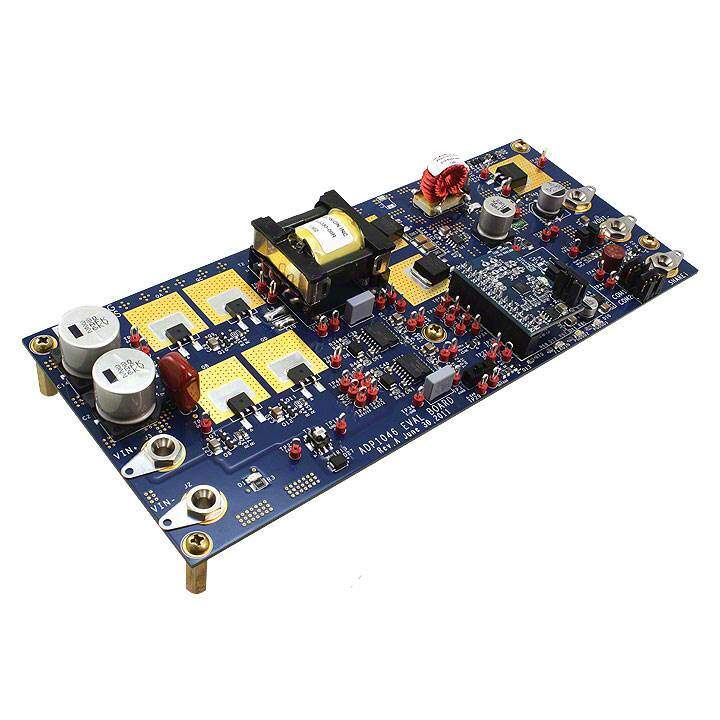
- 型号: ADP1046A-100-EVALZ
- 制造商: Analog
- 库位|库存: xxxx|xxxx
- 要求:
| 数量阶梯 | 香港交货 | 国内含税 |
| +xxxx | $xxxx | ¥xxxx |
查看当月历史价格
查看今年历史价格
ADP1046A-100-EVALZ产品简介:
ICGOO电子元器件商城为您提供ADP1046A-100-EVALZ由Analog设计生产,在icgoo商城现货销售,并且可以通过原厂、代理商等渠道进行代购。 ADP1046A-100-EVALZ价格参考。AnalogADP1046A-100-EVALZ封装/规格:评估和演示板和套件, ADP1046A Power Supply Supervisor/Tracker/Sequencer Power Management Evaluation Board。您可以下载ADP1046A-100-EVALZ参考资料、Datasheet数据手册功能说明书,资料中有ADP1046A-100-EVALZ 详细功能的应用电路图电压和使用方法及教程。
ADP1046A-100-EVALZ 是由 Analog Devices Inc.(亚德诺半导体公司)提供的一款评估板,专为 ADP1046A 数字多相控制器设计。以下是其主要应用场景:

1. 多相电源管理:
   ADP1046A-100-EVALZ 适用于多相降压转换器的设计和评估,支持高电流、低电压的供电需求,例如为高性能处理器(如 FPGA、ASIC 或微处理器)提供稳定的电源。

2. 数字控制与监控:
   该评估板支持通过 PMBus 接口进行数字通信,可以实时监控和调整电源参数,例如输出电压、电流限制、温度等。这种功能非常适合需要精确电源管理的应用场景。

3. 高效能计算设备:
   在服务器、数据中心或网络通信设备中,ADP1046A-100-EVALZ 可用于评估和优化多相电源系统,确保关键组件获得高效的电力供应。

4. 工业自动化:
   在工业应用中,这款评估板可用于开发高可靠性电源解决方案,支持复杂的工业控制系统和高性能电机驱动器。

5. 测试与验证:
   工程师可以利用 ADP1046A-100-EVALZ 来测试不同负载条件下的电源性能,验证设计是否满足特定应用的需求。

6. 教育与研发:
   该评估板也适合用于教学和研究环境,帮助学生和工程师理解数字电源管理技术及其实际应用。

总之,ADP1046A-100-EVALZ 提供了一个灵活且强大的平台,用于评估和优化基于 ADP1046A 控制器的多相电源系统,广泛应用于高性能计算、工业自动化和通信设备等领域。
| 参数 | 数值 |
| 产品目录 | 编程器,开发系统半导体 |
| 描述 | BOARD EVALUATION 100W ADP1046A电源管理IC开发工具 ADP1046A 100W Eval Board |
| 产品分类 | |
| 品牌 | Analog Devices |
| 产品手册 | |
| 产品图片 |
|
| rohs | 符合RoHS无铅 / 符合限制有害物质指令(RoHS)规范要求 |
| 产品系列 | 电源管理IC开发工具,Analog Devices ADP1046A-100-EVALZ- |
| 数据手册 | |
| 产品型号 | ADP1046A-100-EVALZ |
| 主要属性 | - |
| 主要用途 | 电源管理,电源监控器/跟踪器/序列发生器 |
| 产品 | Evaluation Boards |
| 产品种类 | 电源管理IC开发工具 |
| 使用的IC/零件 | ADP1046A |
| 商标 | Analog Devices |
| 嵌入式 | - |
| 工具用于评估 | ADP1046A |
| 所含物品 | 板 |
| 接口类型 | I2C |
| 描述/功能 | 100 W evaluation board |
| 最大工作温度 | + 125 C |
| 最小工作温度 | - 40 C |
| 标准包装 | 1 |
| 用于 | ADP1046A |
| 类型 | Primary/Secondary Side Controllers |
| 系列 | ADP1046A |
| 辅助属性 | - |
| 输入电压 | 36 V to 60 V |
| 输出电压 | 2.5 V |



- 商务部:美国ITC正式对集成电路等产品启动337调查
- 曝三星4nm工艺存在良率问题 高通将骁龙8 Gen1或转产台积电
- 太阳诱电将投资9.5亿元在常州建新厂生产MLCC 预计2023年完工
- 英特尔发布欧洲新工厂建设计划 深化IDM 2.0 战略
- 台积电先进制程称霸业界 有大客户加持明年业绩稳了
- 达到5530亿美元!SIA预计今年全球半导体销售额将创下新高
- 英特尔拟将自动驾驶子公司Mobileye上市 估值或超500亿美元
- 三星加码芯片和SET,合并消费电子和移动部门,撤换高东真等 CEO
- 三星电子宣布重大人事变动 还合并消费电子和移动部门
- 海关总署:前11个月进口集成电路产品价值2.52万亿元 增长14.8%


PDF Datasheet 数据手册内容提取
ADP1046A Evaluation Board User Guide UG-734 One Technology Way • P.O. Box 9106 • Norwood, MA 02062-9106, U.S.A. • Tel: 781.329.4700 • Fax: 781.461.3113 • www.analog.com Wide Input Range, Full Bridge Phase Shifted Topology using the ADP1046A FEATURES CAUTION 600 W phase shifted full bridge topology This evaluation board uses high voltages and currents. Extreme Wide input range to minimize hold up capacitor caution must be taken, especially on the primary side, to ensure Wide ZVS range down to 10% rated load safety for the user. It is strongly advised to power down the Short-circuit and fast overvoltage protection evaluation board when not in use. A current-limited power Remote voltage sensing supply is recommended. Line voltage feedforward ADP1046A EVALUATION BOARD OVERVIEW I2C serial interface to PC Software GUI This evaluation board features the ADP1046A in a switching Programmable digital filters for DCM and CCM power supply application. With the evaluation board and 7 PWM outputs including auxiliary PWM software, the ADP1046A can be interfaced to any PC running Digital trimming Windows® 2000, Windows XP, Windows Vista, Windows NT, Current, voltage, and temperature sense through GUI or Windows 7 via the USB port of the PC. The software allows Calibration and trimming control and monitoring of the ADP1046A internal registers. The evaluation board is set up for the ADP1046A to act as an isolated switching power supply with a rated load of 48 V/12.5 A from an input voltage ranging from 340 V dc to 410 V dc. ADP1046A EVALUATION BOARD PHOTOGRAPH Figure 1. PLEASE SEE THE LAST PAGE FOR AN IMPORTANT WARNING AND LEGAL TERMS AND CONDITIONS. Rev. 0 | Page 1 of 40
UG-734 ADP1046A Evaluation Board User Guide TABLE OF CONTENTS Features .............................................................................................. 1 CS1 Pin Voltage (Primary Current) ......................................... 14 Caution ............................................................................................... 1 Synchronous Rectifier Peak Inverse Voltage .............................. 14 ADP1046A Evaluation Board Overview ....................................... 1 Output Voltage Ripple ............................................................... 15 ADP1046A Evaluation Board Photograph ................................... 1 Transient Voltage at 385 V dc (Nominal Voltage) ................. 16 Revision History ............................................................................... 2 Hold Up Time and Voltage Dropout ....................................... 17 Board Specifications ......................................................................... 3 Line Voltage Feedforward ......................................................... 18 Topology and Circuit Description .................................................. 4 ZVS Waveforms for QA (Passive to Active Transition) ........ 19 Connectors ........................................................................................ 5 ZVS Waveforms for QB (Passive to Active Transition) ......... 20 Setting Files and EEPROM .............................................................. 6 ZVS Waveforms for QC (Passive to Active Transition) ........ 21 Board Evaluation .............................................................................. 7 ZVS Waveforms for QD (Passive to Active Transition) ........ 21 Equipment ..................................................................................... 7 Closed Loop Frequency Response ........................................... 22 Setup ............................................................................................... 7 Efficiency ..................................................................................... 23 Board Settings ............................................................................... 8 Transformer Specifications ........................................................... 24 Theory of Operation During Startup ............................................. 9 Thermal Test Data .......................................................................... 25 Flags Settings Configurations ..................................................... 9 Evaluation Board Schematics and Layout ................................... 27 PWM Settings ................................................................................. 10 Daughter Card PCB Layout ...................................................... 34 Board Evaluation and Test Data ................................................... 11 Register Settings File (.46r) for GUI ............................................ 35 Startup .......................................................................................... 11 Board Settings File (.46b) for GUI ............................................... 37 Overcurrent and Short-Circuit Protection ............................. 12 Ordering Information .................................................................... 38 Primary Gate Driver Dead Time .............................................. 13 Bill of Materials ........................................................................... 38 REVISION HISTORY 10/14—Revision 0: Initial Version Rev. 0 | Page 2 of 40
ADP1046A Evaluation Board User Guide UG-734 BOARD SPECIFICATIONS Table 1. Target Specifications Specification Min Typ Max Unit Notes V 340 385 410 V IN V 48 V OUT I 0.0 12.5 15 A With 400 LFM air flow OUT Overload Current (OCP Limit) 15 A OCP set to shut down PSU after ~10 ms Efficiency 96.35 % Typical reading at 385 V , 12.5 A load IN Switching Frequency 111.6 kHz Output Voltage Ripple 550 mV At 12.5 A load Rev. 0 | Page 3 of 40
UG-734 ADP1046A Evaluation Board User Guide TOPOLOGY AND CIRCUIT DESCRIPTION This evaluation board circuit consists of the ADP1046A in a voltage of 1 V, which is differentially sensed. Output current is typical isolated dc-to-dc switching power supply in a full bridge measured using a sense resistor (R2), which is also differentially phase shifted topology with synchronous rectification. The circuit sensed. To protect the synchronous rectifiers from exceeding provides a rated output load of 48 V/12.5 A from a nominal the peak reverse voltage, an RCD clamp is implemented (D58, input voltage of 385 V dc operated in continuous conduction D59, R112 to R115, and C94). mode (CCM) at all times. The ADP1046A provides functions The primary current is sensed through the CS1 pin with a small such as output voltage regulation, output overvoltage protection, RC time constant (R44 and C22) that acts as a low-pass filter to input and output current protection, primary cycle by cycle remove the high frequency noise on the signal. An additional protection, and overtemperature protection. Figure 70 provides RC can be placed; however, the internal Σ-Δ analog-to-digital a top level schematic that describes the power flow and auxiliary converter (ADC) naturally averages the signal. The position of power supply that starts up at 50 V dc and provides power to the current transformer is placed in series with the resonant the ADP1046A through a 3.3 V low dropout regulator (LDO), inductor to avoid saturation. the iCoupler® isolation plus gate drivers, the on-board fan, and Line voltage feedforward is implemented using an RCD circuit the synchronous rectifier drivers. The auxiliary power supply (D13, R59, R64, C38, and C43) that detects the peak voltage at using the transformer (T3) and IC (U10) generates a 12 V rail the synchronous field effect transistor (FET). There are two on the primary side and a 13 V rail on the secondary side. The time constants that can be implemented in series with each main power transformer (T12) provides a wide input voltage other. The time constants must be matched such that it retains range (340 V dc to 410 V dc), and the circuit has a wide zero the peak value during the switching frequency period, but also voltage switching (ZVS) range down to 10% of the rated load. is not too long in case there is a step down change in the input The primary side consists of the input terminals (JP8 and JP9), voltage. This peak voltage is further ratioed and fed in the the switches (Q1 to Q4), the current sense transformer (T5), ACSNS pin of the controller (ADP1046A). A thermistor (RT1) and the main transformer (T1). There is also a resonant inductor is placed on the secondary side close to the synchronous FET that aids in zero voltage switching at lighter load conditions. and acts as thermal protection for the power supply. A 16.5 kΩ The ADP1046A is situated on the secondary side and is powered resistor is placed in parallel with the thermistor that allows the via the auxiliary power supply, or the USB connector via the software GUI to read the temperature directly in degrees Celsius. LDO. The gate signal for the primary switches is generated by Capacitor C69 is a YCAP that reduces common-mode noise the ADP1046A through the iCouplers and fed into the MOSFET from the transformer. drivers (U17 and U18). Bypass capacitors (C71, C72, and C114 to 116) are placed closed to the primary switches. Diodes (D36 Also available on the secondary side is a 4-pin connector for and 37) clamp the resonance between the resonant inductor and I2C communication. This connector allows the PC software to the output capacitance (COSS) of the output rectifiers. communicate with the IC through the USB port of the PC. The user can easily change register settings on the ADP1046A and The secondary (isolated) side of the transformer consists of a monitor the status registers. It is recommended that the USB center tapped winding. The synchronous rectifier driver (U7) dongle be connected directly to the PC, and not via the external provides the drive signals for the switches (Q9 and Q23). The hub. output inductor (L8) and output capacitor (C11 and C41) act as a low-pass filter for the output voltage. The output voltage is fed Switch SW2 acts as a hardware PS_OFF switch. The polarity is back to the ADP1046A using a voltage divider and has a nominal configured using the GUI to be active high. Rev. 0 | Page 4 of 40
ADP1046A Evaluation Board User Guide UG-734 CONNECTORS Table 2 lists the connectors on the board. Table 3 lists the Table 3. I2C Connector Pinout Descriptions pinouts of the USB to I2C adapter, shown in Figure 2. Pin (Left to Right) Function Table 2. Board Connectors 1 5 V 2 SCL Connector Evaluation Board Function 3 SDA J8 DC input positive terminal 4 Ground J9 DC input negative terminal J11 Output voltage positive terminal J12 Output voltage negative terminal J16 Socket for auxiliary power supply J18 I2C connector Figure 2. I2C Connector (Pin 1 on Left) Figure 3. ADP1046A Evaluation Board (Side View) Figure 4. Evaluation Board (Top View) Rev. 0 | Page 5 of 40
UG-734 ADP1046A Evaluation Board User Guide SETTING FILES AND EEPROM The ADP1046A communicates with the GUI software using the enable/disable, primary current, output voltage, and current, I2C bus. can therefore be digitally monitored and controlled using the software only. Always make sure that the correct board file has The register settings (having the extension .46r) and the board been loaded for the board currently in use. settings (having the extension .46b) are two files that are associated with the ADP1046A software. The register settings file contains Each ADP1046A chip has trim registers for the temperature, information such as the overvoltage and overcurrent limits, the soft the input current, the output voltage and current, and ACSNS. start timing, and the PWM settings that govern the functionality of These values can be configured during production and are not the device. The ADP1046A stores all its settings in the EEPROM. overwritten when a new register settings file is loaded. Therefore, the trimming of all the ADCs for that corresponding environmental The EEPROM on the ADP1046A does not contain any and circuit condition (such as component tolerances or thermal information about the board, such as the current sense resistor, drift) are retained. A guided Auto Trim Wizard starts up, which output inductor, and capacitor values. This information is stored in trims the previously mentioned quantities so that the measurement the board setup file (extension .46b) and is necessary for the value matches the values displayed in the GUI to allow ease of GUI to display the correct information in the Monitor tab as control through the software. well as the Filter Settings window. The entire status of the power supply, such as the ORFET and synchronous rectifiers Figure 5. ADP1046A and GUI Interaction Rev. 0 | Page 6 of 40
ADP1046A Evaluation Board User Guide UG-734 BOARD EVALUATION EQUIPMENT 6. If the software does not detect the device, it enters into simulation mode. Ensure that the connecter is connected The following equipment is required: to the daughter card. Click the Scan for ADP1046A Now A dc power supply (300 V to 400 V, 600 W) icon located on the top right hand corner of the screen, as An electronic load (60 V/600 W) shown in Figure 7. An oscilloscope with differential probes A PC with ADP1046A GUI installed Precision digital voltmeters (HP34401or equivalent, 6 digits) for measuring dc current and voltage SETUP Take the following steps to set up the evaluation board. Do not choans nfiencits thheed U inSBst aclalbinleg t. o the evaluation board until the software ADSPC10A4N6 AF ONROW DASSEHTTBIONAGRSD LOSAEDT TBINOGASRD 12489-007 Figure 7. GUI Icons 1. Install the ADP1046A software by inserting the installation CD. The software setup starts automatically, and a guided 7. Click the Load Board Settings icon (see Figure 7) and process installs the software as well as the USB drivers for select the ADP1046A_FBPS_600W_xxxx.46b file. This file communication between the GUI and the IC using the contains all the board information, including values of USB dongle. shunt and voltage dividers. Note that all board setting files 2. Insert the daughter card in Connector J16 as shown in have a .46b file extension. Figure 72. 8. The IC on the board comes preprogrammed, and this step 3. Ensure that the PS_ON switch (SW1 on the schematic) is is optional. The original register configuration is stored in turned to the off position. The switch is located on the the ADP1046A_FBPS_600W_xxxx.46r register file (note bottom left half of the board. that all register files have a .46r file extension). The file can 4. Connect one end of USB dongle to the board and the other be loaded using the second icon from the left in Figure 8. end to the board to the USB port on the PC using the USB 9. Connect a dc power source (385 V dc nominal, current to I2C interface dongle. limit to approximately 2 A) and an electronic load at the 5. The software reports that the ADP1046A has been located output set to 1 A. on the board. Click Finish to proceed to the main software 10. Connect a voltmeter on test points TP26(+) and TP46(−). interface window. The serial number reported on the side Ensure that differential probes are used and that the ground of of the checkbox indicates the USB dongle serial number, as the probes are isolated if oscilloscope measurements are shown in Figure 6. The windows also displays the device made on the primary side of the transformer. I2C address. 11. Click the Dashboard Settings icon (see Figure 7) and turn on the software PS_ON. 12. The board is running and ready for evaluation. The output now reads 12 V dc. 13. Click the Monitor tab and then click the Flags and readings icon. This window provides a snapshot of the entire state of the PSU in a single user friendly window. Figure 6. ADP1046A Address of 50h in the GUI Figure 8. Different Icons on Dashboard for Loading and Saving .46r and .46b Files Rev. 0 | Page 7 of 40
UG-734 ADP1046A Evaluation Board User Guide BOARD SETTINGS Figure 9 shows the board settings. 12489-009 Figure 9. Main Setup Window of ADP1046A GUI Rev. 0 | Page 8 of 40
ADP1046A Evaluation Board User Guide UG-734 THEORY OF OPERATION DURING STARTUP The following steps briefly describe the startup procedure of the 4. The PSU now is running in steady state. PGOOD1 turns ADP1046A, the power supply, and the operation of the state on after the programmed debounce. machine for the preprogrammed set of registers that are included 5. If a fault is activated during the soft start or steady state, in the design kit. the corresponding flag is set, and the programmed action is taken, such as Disable Power Supply and Re-enable 1. The on-board auxiliary power starts up at approximately after 1 s, Disable SR and OrFET, or Disable OUTAUX 50 V dc. The on-board auxiliary power provides a drive (see Figure 10). voltage on the isolated side to an LDO (3.3 V) that powers up the ADP1046A. After VDD (3.3 V) is applied to the FLAGS SETTINGS CONFIGURATIONS ADP1046A, it takes approximately 20 μs to 50 μs for When a flag is triggered, the ADP1046A state machine waits for VCORE to reach 2.5 V. The digital core is now activated, a programmable debounce time before taking any action. The and the contents of the registers are downloaded in the response to each flag can be programmed individually. The EEPROM. The ADP1046A is now ready for operation. flags can be programmed in a single window by selecting the 2. PS_ON is applied. The power supply begins the Flag Settings icon under the Monitor tab in the GUI. This programmed soft start ramp of 50 ms (programmable). monitor window shows all the fault flags (if any) and the 3. Because the soft start from precharge setting is active, the readings in one page. The Get First Flag button determines the output voltage is sensed before the soft start ramp begins. first flag that was set in the case of a fault event. Depending on the output voltage level, the effective soft start ramp is reduced by the proportional amount. 12489-010 Figure 10. Fault Configurations Rev. 0 | Page 9 of 40
UG-734 ADP1046A Evaluation Board User Guide PWM SETTINGS The ADP1046A has a fully programmable PWM setup that Each PWM edge can be moved in 5 ns steps to achieve the controls seven PWMs. Due to this flexibility, the IC can appropriate dead time required, and the maximum modulation function in several different topologies, such as any isolated limit sets the maximum duty cycle. buck derived topology, push-pull, and flyback, and also has the control law for resonant converters. 12489-011 Figure 11. PWM Settings Window in the GUI Table 4. PWMs and Their Corresponding Switching Element PWM Switching Element Being Controlled OUTA to OUTD Primary switch PWM configured for phase shifted topology SR1, SR2 Synchronous rectifier PWMs OUTAUX Not applicable Rev. 0 | Page 10 of 40
ADP1046A Evaluation Board User Guide UG-734 BOARD EVALUATION AND TEST DATA STARTUP Figure 12. Startup at 340 V dc, 600 W Load (Software PS_ON) Figure 14. Startup at 385 V dc, Full Load Green Trace: Output Voltage, 10 V/div, 10 ms/div Green Trace: Output Voltage, 10 V/div, 10 ms/div Yellow Trace: Load Current, 2 A/div, 10 ms/div Yellow Trace: Primary Current, 2 A/div, 10 ms/div Red Trace: Input Voltage, 50 V/div, 10 ms/div Figure 13. Startup at 385 V dc, 600 W Load (Software PS_ON) Figure 15. Primary Current at Full Load Green Trace: Output Voltage, 10 V/div, 10 ms/div Red Trace: Resonant Inductor Current, 1 A/div, 2 μs/div Yellow Trace: Load Current, 2 A/div, 10 ms/div Yellow Trace: Primary Current, 1 A/div, 2 μs/div Red Trace: Input Voltage, 50 V/div, 10 ms/div Rev. 0 | Page 11 of 40
UG-734 ADP1046A Evaluation Board User Guide OVERCURRENT AND SHORT-CIRCUIT PROTECTION Figure 16. OCP at 385 V dc, 15 A Load (Action to Shutdown After ~10 ms) Figure 18. OCP at 385 V dc, 600 W to Output Shorted Green Trace: Output Voltage, 10 V/div, 5 ms/div Red Trace: SR Drive, 5 V/div, 5 ms/div Yellow Trace: Load Current, 5 A/div, 5 ms/div Green Trace: Output Voltage, 10 V/div, 200 μs/div Red Trace: Input Voltage, 50 V/div, 5 ms/div Yellow Trace: Output Current, 5 A/div Figure 17. OCP at 350 V dc, 15 A Load (Action to Shutdown After ~10 ms) Figure 19. OCP, Hiccup Mode, 385 V dc, 600 W to Output Shorted Green Trace: Output Voltage, 10 V/div, 5 ms/div Red Trace: SR Drive, 5 V/div, 5 ms/div Yellow Trace: Load Current, 5 A/div, 5 ms/div Green Trace: Output Voltage, 10 V/div, 200 μs/div Red Trace: Input Voltage, 50 V/div, 5 ms/div Yellow Trace: Output Current, 5 A/div Rev. 0 | Page 12 of 40
ADP1046A Evaluation Board User Guide UG-734 PRIMARY GATE DRIVER DEAD TIME Figure 20. Primary Gate Drive Voltage at Maximum Modulation Figure 23. Primary Gate Drive Voltage at Minimum Modulation (Output of iCoupler), 5 V/div, 1 μs/div (Output of iCoupler), 5 V/div, 1 μs/div Yellow Trace: OUTA, Red Trace: OUTB, Blue Trace: OUTC, Green Trace: OUTD Yellow Trace: OUTA, Red Trace: OUTB, Blue Trace: OUTC, Green Trace: OUTD Figure 21. Primary Gate Drive Voltage at Maximum Modulation Figure 24. Primary Gate Drive Voltage at Minimum Modulation (Output of iCoupler) Showing Dead Time, Zoom In, 5 V/div, 0.2 μs/div (Output of iCoupler) Showing Dead Time, Zoom In, 5 V/div, 0.2 μs/div Yellow Trace: OUTA, Red Trace: OUTB, Blue Trace: OUTC, Green Trace: OUTD Yellow Trace: OUTA, Red Trace: OUTB, Blue Trace: OUTC, Green Trace: OUTD Figure 22. Primary Gate Drive Voltage at Maximum Modulation Figure 25. Primary Gate Drive Voltage at Minimum Modulation (Output of iCoupler) Showing Dead Time, Zoom In, 5 V/div, 0.2 μs/div (Output of iCoupler) Showing Dead Time, Zoom In, 5 V/div, 0.2 μs/div Yellow Trace: OUTA, Red Trace: OUTB, Blue Trace: OUTC, Green Trace: OUTD Yellow Trace: OUTA, Red Trace: OUTB, Blue Trace: OUTC, Green Trace: OUTD Rev. 0 | Page 13 of 40
UG-734 ADP1046A Evaluation Board User Guide CS1 PIN VOLTAGE (PRIMARY CURRENT) SYNCHRONOUS RECTIFIER PEAK INVERSE VOLTAGE Figure 26. Primary Current at 385 V dc, 300 W Load, 2 μs/div Figure 28. Synchronous Rectifier MOSFET Peak Reverse Voltage Yellow Trace: Primary Current Half Effect Probe, 1 A/div at 600 W Load, 385 V dc, 50 V/div, 2 μs/div Green Trace: CS1 Pin Voltage, 270 mV/div Figure 27. Primary Current at 385 V dc, 600 W Load, 2 μs/div Figure 29. Synchronous Rectifier MOSFET Peak Reverse Voltage Yellow Trace: Primary Current Half Effect Probe, 1 A/div at 600 W Load, 385 V dc, 50 V/div, 500 ns/div Green Trace: CS1 Pin Voltage, 270 mV/div Rev. 0 | Page 14 of 40
ADP1046A Evaluation Board User Guide UG-734 OUTPUT VOLTAGE RIPPLE Figure 30. Output Voltage AC-Coupled, 385 V dc, 12.5 A, 500 mV/div, Figure 31. Output Voltage AC-Coupled, 385 V dc, 12.5 A, 500 mV/div, 20 μs/div, High Frequency Component 2 ms/div, Low Frequency Component Rev. 0 | Page 15 of 40
UG-734 ADP1046A Evaluation Board User Guide TRANSIENT VOLTAGE AT 385 V dc (NOMINAL VOLTAGE) Load Step of 15% to 50% Load Step of 50% to 100% Figure 32. Output Voltage Transient, 500 μs/div Figure 34. Output Voltage Transient, 500 μs/div Yellow Trace: Load Current, 2 A/div Yellow Trace: Load Current, 2 A/div Green Trace: Output Voltage (AC-Coupled), 500 mV/div Green Trace: Output Voltage (AC-Coupled), 500 mV/div Figure 33. Output Voltage Transient, 500 μs/div Figure 35. Output Voltage Transient, 500 μs/div Yellow Trace: Load Current, 2 A/div Yellow Trace: Load Current, 2 A/div Green Trace: Output Voltage (AC-Coupled), 500 mV/div Green Trace: Output Voltage (AC-Coupled), 500 mV/div Rev. 0 | Page 16 of 40
ADP1046A Evaluation Board User Guide UG-734 Load Step of 0% to 50% HOLD UP TIME AND VOLTAGE DROPOUT Figure 36. Output Voltage Transient, 500 μs/div Figure 38. Minimum Input Voltage of ~330 V dc Before Output Regulation is Yellow Trace: Load Current, 2 A/div Lost at 600 W, 10 ms/div Green Trace: Output Voltage (AC-Coupled), 500 mV/div Red Trace: Input Voltage Step, 50 V/div Green Trace: Output Voltage, 10 V/div Figure 37. Output Voltage Transient, 500 μs/div Figure 39. Hold Up Time of ~10.781 ms Before Output Voltage Reaches 36 V Yellow Trace: Load Current, 2 A/div (Minimum Telecom Input) at 600 W, 100 μF Input Capacitor,10 ms/div Green Trace: Output Voltage (AC-Coupled), 500 mV/div Red Trace: Input Voltage Step, 50 V/div Green Trace: Output Voltage, 10 V/div Rev. 0 | Page 17 of 40
UG-734 ADP1046A Evaluation Board User Guide LINE VOLTAGE FEEDFORWARD Figure 40. Line Voltage Feedforward Disabled, 600 W Load Figure 42. Line Voltage Feedforward Disabled, 600 W Load Red Trace: Input Voltage Step, 350 V dc to 385 V dc, 50 V/div Red Trace: Input Voltage Step, 350 V dc to 385 V dc, 50 V/div Green Trace: Output Voltage (AC-Coupled), 200 mV/div Green Trace: Output Voltage (AC-Coupled), 200 mV/div Figure 41. Line Voltage Feedforward Enabled, 600 W Load Figure 43. Line Voltage Feedforward Enabled, 600 W Load Red Trace: Input Voltage Step, 350 V dc to 385 V dc, 50 V/div Red Trace: Input Voltage Step, 350 V dc to 385 V dc, 50 V/div Green Trace: Output Voltage (AC-Coupled), 200 mV/div Green Trace: Output Voltage (AC-Coupled), 200 mV/div Rev. 0 | Page 18 of 40
ADP1046A Evaluation Board User Guide UG-734 ZVS WAVEFORMS FOR QA (PASSIVE TO ACTIVE TRANSITION) Figure 44. Resonant Transition at No Load, 100 ns/div Figure 46. Resonant Transition at 300 W Load, 100 ns/div Red Trace: VDS of QA, 100 V/div Red Trace: VDS of QA, 100 V/div Yellow Trace: VGS of QA, 5 V/div Yellow Trace: VGS of QA, 5 V/div Figure 45. Resonant Transition at 48 W Load, 100 ns/div Figure 47. Resonant Transition at 600 W Load, 100 ns/div Red Trace: VDS of QA, 100 V/div Red Trace: VDS of QA, 100 V/div Yellow Trace: VGS of QA, 5 V/div Yellow Trace: VGS of QA, 5 V/div Rev. 0 | Page 19 of 40
UG-734 ADP1046A Evaluation Board User Guide ZVS WAVEFORMS FOR QB (PASSIVE TO ACTIVE TRANSITION) Figure 48. Resonant Transition at No Load, 100 μs/div Figure 50. Resonant Transition at 300 W Load, 100 μs/div Red Trace: VDS of QB, 100 V/div Red Trace: VDS of QB, 100 V/div Yellow Trace: VGS of QB, 5 V/div Yellow Trace: VGS of QB, 5 V/div Figure 49. Resonant Transition at 48 W Load, 100 μs/div Figure 51. Resonant Transition at 600 W Load, 100 μs/div Red Trace: VDS of QB, 100 V/div Red Trace: VDS of QB, 100 V/div Yellow Trace: VGS of QB, 5 V/div Yellow Trace: VGS of QB, 5 V/div Rev. 0 | Page 20 of 40
ADP1046A Evaluation Board User Guide UG-734 ZVS WAVEFORMS FOR QC (PASSIVE TO ACTIVE ZVS WAVEFORMS FOR QD (PASSIVE TO ACTIVE TRANSITION) TRANSITION) Figure 52. Resonant Transition at 300 W Load, 200 μs/div Figure 54. Resonant Transition at 0 A Load, 100 μs/div Red Trace: VDS of QC, 100 V/div Red Trace: VDS of QD, 100 V/div Yellow Trace: VGS of QC, 5 V/div Yellow Trace: VGS of QD, 5 V/div Figure 53. Resonant Transition at 600 W Load, 200 μs/div Figure 55. Resonant Transition at 300 W Load, 100 μs/div Red Trace: VDS of QC, 100 V/div Red Trace: VDS of QD, 100 V/div Yellow Trace: VGS of QC, 5 V/div Yellow Trace: VGS of QD, 5 V/div Rev. 0 | Page 21 of 40
UG-734 ADP1046A Evaluation Board User Guide CLOSED LOOP FREQUENCY RESPONSE A network analyzer (AP200) was used to test the bode plots of the with the output voltage divider using an isolation transformer. system. A continuous noise signal of 300 mV was injected across The operating condition was 385 V dc input and a load condition the entire frequency range across a 10 Ω resistor in series (R35) of 600 W with a soaking time of 45 minutes. Figure 56. Bode Plots, 385 V dc Input, 12.5 A Load, Blue Trace: Gain in dB, Red Trace: Phase in Degrees, Crossover Frequency = 3.15 kHz, Phase Margin = 115.2° Rev. 0 | Page 22 of 40
ADP1046A Evaluation Board User Guide UG-734 EFFICIENCY 0.98 96.8 96.7 0.94 96.6 %) 0.90 %) CY ( EFFICIENCY AT 385V dc CY ( 96.5 EN 0.86 95% EN FICI FICI 96.4 F F E 0.82 E 96.3 0.78 96.2 0.740.5 2.5 4.5 LOAD6 .C5URREN8T.5 (A) 10.5 12.513.5 12489-057 96.1340 350 3I6N0PUT VO3L7T0AGE (V 3d8c0) 390 400 12489-058 Figure 57. Efficiency vs. Load at 385 V dc, 45 Minute Soaking Time, Figure 58. Efficiency vs. Line Voltage at 600 W Load with On-Board Airflow Rev. 0 | Page 23 of 40
UG-734 ADP1046A Evaluation Board User Guide TRANSFORMER SPECIFICATIONS Table 5. Transformer Specifications Parameter Min Typ Max Unit Notes Core and Bobbin PQ3535, Magnetics, Inc., material or equivalent Primary Inductance 3.316 mH Pin 1 to Pin 6 Leakage Inductance 4 μH Pin 1 to Pin 6 with all other windings shorted Resonant Frequency 850 kHz Pin 1 to Pin 6 with all other windings open 6 11, 12 3 7, 8 1 5T, COPPER FOIL, 10mil 14T, 75 STRANDS, 40AWG, LITZ WIRE 11, 12 3 9, 10 7, 8 14T, 75 STRANDS, 40AWG, LITZ WIRE 6 5T, COPPER FOIL, 10mil 9, 10 7, 8 12489-059 31 12489-060 Figure 59. Transformer Electrical Diagram Figure 60. Transformer Construction Diagram Rev. 0 | Page 24 of 40
ADP1046A Evaluation Board User Guide UG-734 THERMAL TEST DATA A thermal snapshot of the evaluation board was taken after running at 600 W with a 45 minute soaking time. Figure 61. Thermals, Complete Board Figure 64. Thermals, Output Inductor Figure 62. Thermals, Primary Clamp Diode Figure 65. Thermals, Output Current Sense Resistor Figure 63. Thermals, Synchronous Rectifier Figure 66. Thermals, Transformer Rev. 0 | Page 25 of 40
UG-734 ADP1046A Evaluation Board User Guide Figure 67. Thermals, Resonant Inductor Figure 69. Thermals, Transformer Figure 68. Thermals, Primary MOSFET Rev. 0 | Page 26 of 40
ADP1046A Evaluation Board User Guide UG-734 EVALUATION BOARD SCHEMATICS AND LAYOUT 344100TVVO ddcc BPFRHUIADLSGLEE SRYENCCT 47P82OV0WW dE cOR/6V0E0RWL,OAD SHIFTED MOSFET I2C INTERFACE DRIVERS ADP1046A DAUGHTER CARD SOCKET MOSFET DRIVERS 3.3V LDO OR 5V FROM USB 3.3V ADuM4223 iCoupler + OUTA TO OUTD DRIVER VDD_PRI = 12V AUXILLARY PSU VDD_SEC = 13V SEPCROIMNADRAYR Y= =+ 1+21V3V 12489-070 Figure 70. Schematic, Top Level Rev. 0 | Page 27 of 40
UG-734 ADP1046A Evaluation Board User Guide J11VOUT+ 54J13VOUT J12VOUT- 170-98421 1 1nF2 PGND 1 C1 TP46VOUT- 1 TP26VOUT+ C6810uF63V C7010uF C7310uF C7610uF C7710uF C7810uF63V PGND VS1 2C11330uF63V C41680uF163VTP39VS3+VS3-C7910uF63VVS3+C8010uFTP41VS3- R117C8110uF0 2C8310uF C8410uF163VCSNL1206FT2L0012R2220.002 11 CS2-CS2+ UTPUT CURRENT & VOLTAGE SENSING TP48TP50TP47TP49TP52GNDGNDGNDGNDVSS PRI_GNDVSSPGND O Vin_AuxPRIMARYSECONDARYL84.7uH1225A2TP14QCC111C114C116R130G-QCT650V12.2uF17TP271uF1uF220.7A5GATE_QC+100VGQ23/D36D33E3F600VC12021-C3AJ2R1160.1uF023D556SOUTAUXR651N4148N100V010k02A2PQ23PRI_GNDD62PGATE_QC-R122BSC22DN20NS3 GS1N5819200V 7A10k11L61221112T519233UHC752M-28285-0330104Q220.022UFB51.25KVDCIPB107N20N3 GSR2_out34176C200V1:100PE-6710088AR1091T12338PQ353521CS-CS+QDD37TP16650VR131S3J-E3/57TG-QB20.7A123600V2DGATE_QD+3A2FC3Q922200V21088A6IPB107N20N3 GD54D59D58N1R6801N4148VSSES1DES1D210k250V250VPP1A1AR111S1112R112 91kVS1R113 91k 1R114 91kSR1_outC69R115 91k2200pF500VACGATE_QD-C9433nF200VNot needed in Resonant mode due to softswitching:R112, R113, R114, D58, D59, C94, L8D10PRI_GNDVSSQ9, Q22 can be replaced by 200V diodesR128RS1JVSS4.9921 +3.3V600V1AC20C19U171uF0.1uFADuM4223ARWZ25V25V116OUTAVIAVDDA215R420GATE_QA+VIB_U17VIBVOA314GATE_QA-VDD1GNDA413GND1NC4512DISABLENC3611VDD_PRIC15NC1VDDB710R4301uFGATE_QB+NC2VOB89GATE_QB-VDD2GNDB25VC18C171uF0.1uFAGND25V PRI_GND D11R129RS1J4.9921 +3.3V600V1AC31C30U181uF0.1uFADuM4223ARWZ25V25V116OUTCVIAVDDAR490215GATE_QC+VIB_U18VIBVOA314GATE_QC-VDD1GNDA413GND1NC4512DISABLENC3611VDD_PRIC16NC1VDDBR4507101uFGATE_QD+NC2VOB89GATE_QD-VDD2GNDB25VC29C211uF0.1uFAGND25V PRI_GNDGATE DRIVERS FOR PRIMARY FETS 1 LS Vin_400VC71F2QAC720.33uFSPP20N60CFD0.33uF5A450V450V650V 20.7A1TP132250VAC 3AG-QA#0875003R13312TP4Vin+3GATE_QA+21C115D52PRI_GND1uFR341N4148630VC10610k100uF400VGATE_QA- QBSPP20N60CFD650V 20.7A2TP15R132G-QB12GATE_QB+321D53R25TP121N414810kVin- 12 PRI_GND1 GATE_QB- J8VIN+ J9VIN- Figure 71. Schematic, Main Power Train Rev. 0 | Page 28 of 40
ADP1046A Evaluation Board User Guide UG-734 J18 1VIN_AUX12VIN_AUX23PRI_GND14PRI_GND25PRI_GND36PRI_GND47VDD_PRI18VDD_PRI29PRI_GNDNC110NC211NC312NC413PGND114PGND215VDD_SEC116VDD_SEC2PGND AUXILLARU PSUPRIMARY +12VSECONDARY +12V J16COM115V2SCL3SDA4GND J17COM21SCL2GND A3SDA4VBUS5SPI MISO6NC7SPI SCLK8SPI MOSI9SPI CS A10GND B Miro MaTchAGND 270-98421 400V CC8414DBMM AC8414DBMM +5V 84D 05D Vin_Aux VDD_PRI VDD_SEC 3 21 12 3 AGND 1 D471N4148 2 FAN CONTROL3Part #: 3106KL-04W-B50-B01Q21120X120X25MM 48VDCBSS138 1 PGND +5V R95 100C63C6033pF33pF R96AGND 100C62C6133pF33pF AGND RFACE AND FILTERING E 2 NT VDD_SECJ28 1122 R87100 OUTAUX CS+ CS- SCL SDA 2IC I TEMP SENSING RTDRTD2R71100k0Q101MMBT3904 3R7016.5k R740AGND R44D6402MMBD4148SE31 R52C22R7622K1000pF10231D63GMMBD4148SECS1 SENSING C 21BD13R592001N4148 LINE FEED-FORWARD D13 = DNI for Resonant modeR66 = 0 for Resonant modeΩchange ACSNS resistor dividerR73 0accordingly to give >0.45V on DC AGNDPGND D49YELLOW1 1 D51REDAGNDED INDICATORS TP23CS1CS1 11 D20D19DNI2.5V22 MMSZ5222BT1 PGND R66 DNI R64 0 C38C43DNIDNI PGND 2 2 L SHAREO SHAREI SDA SCL FLAGIN R40 2k2 R93 2k2 OUTAUX OUTC OUTA CS2- CS2+ VS1 VS2 GATE VS3+ VS3- +5V +3.3V VDD_SEC PGOOD2 PGOOD1 ACSNS PGND AGND NNECTIONS O J15ADP1046_DC1SHAREO 2SHAREI3SDA4SCL 5RTD6FLAGIN 7PGOOD28PGOOD1 PSON 10OUTAUX OUTD 12OUTC OUTB14OUTA 15CS116ACSNS SR1 SR219CS2- 20CS2+21PGND 22VS123VS224GATE 25VS3+26VS3- 275V283.3V29AGND 3012V GHTER CARD C 9 11 13 17 18 DAU PSONSW2PSON 1nFC74R78 0 R79 DNIGND R75 0VIB_U17R77 DNIVIB_U18 SR1SR2U7ADP365427INAOUTA45INBOUTB16NC1VDD 38C44PNDNC24.7uFVSS GATE DRIVERS FOR SRVSS ADP1046A A +3.3V SR1_out SR2_out VDD_SEC C82 0.1uF Figure 72. Schematic, Miscellaneous Rev. 0 | Page 29 of 40
UG-734 ADP1046A Evaluation Board User Guide SHAREi SHARE0 PGOOD1 PGOOD2 FLAGIN PSON SDA SCL J7 370-98421 +3.3V R142.2k 1 2 3 4 3 kk22..22 5213RR R242.2k +3.3V +5V SCL SDA R332.2k 24 23 22 21 20 19 18 17 R292.2k 4 SHAREi SHAREo PGOOD1 PGOOD2 FLAGIN PSON SDA SCL DGND RTD+3.3V 2C110.1uF 3 kk00113F6pC090213RR3 795806223222 SDDDDEEDDTNRRRVAGODCV U1 ADP1046A XUCDABAETTTTTTUUUUUAOOOOOG 125346111111 BADCXETTTTUTUUUUAAOOGOOTUO R130 Ohm AGNDPGND VS3- 13 -3SV 2RS 01 2RS 23 +3SV 1RS 9 1RS C7DNI C9DNI VS2 AGND VS1 CS2- CS2+ ACSNS CS1 PGND 33 DAP VS3+ R1046.4k R111k C14C30.1uFDNI C41DNI 2 3 4 5 6 7 8C151000pF 5.1K 2 D6LEDRED 1 VS2 R7 46.4k R81k CS1 +3.3V R21 C124.7uF C1DNI C2DNI C80.1uF 12 3 4 VS1 CS2- 2 R5C1646.4kR3DNI4.99kR61kC13100pF +5V 2 D21N4148 1 8OUTIN7OUTIN 6NRERR 5GNDSD U2 ADP3303 CS2+ 2 C17R44.99kDNI C10100pF +12V 2 D11N4148 1 C51.0uF50V ACSNS R165k R21k C18DNI +12V +3.3V +5V VS3- VS3+ GATE VS2 VS1 CS2+ CS2- SR2 SR1 ACSNS CS1 OUTA OUTB OUTC OUTD OUTAUX PSON PGOOD1 PGOOD2 FLAGIN RTD SCL SDA SHAREi SHAREo C16C17 DNIDNI 33pF33pF C13 DNI DNI J130 29Analog GND 28 27 26Inverting Remote Voltage Sense Input 25Noninverting Remote Voltage Sense Input 24OrFET Gate Drive Output 23OrFET Drain Sense Input 22Local Voltage Sense Input 21Power GND 20Noninverting Differential Current Sense Input 19Inverting Differential Current Sense Input 18Synchronous Rectifier Output 17Synchronous Rectifier Output 16AC Sense Input 15Primary Side Differential Current Sense Input 14PWM Output for Primary Side Switch 13PWM Output for Primary Side Switch 12PWM Output for Primary Side Switch 11PWM Output for Primary Side Switch 10Auxiliary PWM Output 9Power Supply On Input 8Power Good Output (Open Drain) 7Power Good Output (Open Drain) 6Flag Input 5Thermistor Input 42IC Serial Clock Input 32IC Serial Data Input and Output 2Analog Share Bus Feedback Pin 1Share Bus Output Voltage 4Short trace from pin 25 DGND to pin 2 AGND ADDR19 = 10k 1%3 SHARE O/IR33, R32 = 2.2k 1% PGOOD1/2R14, R15 = 2.2k 1% VCOREC26 = 330pF 50V X7R R3R4C102 Low Side4.99k4.99kDNI High Side110k110kDNI 1: R3, R4, R5, R6, R7, R8, R10, R11,R20 ARE 0.1% 25ppm UNLESS OTHERWISE SPECIFIED. Figure 73. Schematic, ADP1046A Daughter Card Rev. 0 | Page 30 of 40
ADP1046A Evaluation Board User Guide UG-734 Figure 74. Top Side Placement of Components Figure 75. Bottom Side Placement of Components Rev. 0 | Page 31 of 40
UG-734 ADP1046A Evaluation Board User Guide Figure 76. Layout Layer 1 Figure 77. Layout Layer 2 Rev. 0 | Page 32 of 40
ADP1046A Evaluation Board User Guide UG-734 Figure 78. Layout Layer 3 Figure 79. Layout Layer 4 Rev. 0 | Page 33 of 40
UG-734 ADP1046A Evaluation Board User Guide DAUGHTER CARD PCB LAYOUT Figure 80. PCB Assembly, Top Figure 83. PCB Layout, Layer 3 Figure 81. PCB Layout, Top Layer Figure 84. PCB Layout, Bottom Layer Figure 82. PCB Layout, Layer 2 Figure 85. PCB Layout, Silkscreen Bottom Rev. 0 | Page 34 of 40
ADP1046A Evaluation Board User Guide UG-734 REGISTER SETTINGS FILE (.46r) FOR GUI Copy the contents below into a text file and rename it using a .46r file extension. Load this file in the GUI using the Load Register Settings option. Ensure that the last line of the .46r file does not have a carriage return. Reg(8h) = F3h - Fault Configuration Register 1 Reg(4Ch) = A8h - PWM 3 Negative Edge Setting Reg(9h) = 7Dh - Fault Configuration Register 2 Reg(4Dh) = 5h - PWM 4 Positive Edge Timing Reg(Ah) = 58h - Fault Configuration Register 3 Reg(4Eh) = 8h - PWM 4 Positive Edge Setting Reg(Bh) = 0h - Fault Configuration Register 4 Reg(4Fh) = 38h - PWM 4 Negative Edge Timing Reg(Ch) = 88h - Fault Configuration Register 5 Reg(50h) = A8h - PWM 4 Negative Edge Setting Reg(Dh) = 88h - Fault Configuration Register 6 Reg(51h) = 3Dh - SR 1 Positive Edge Timing Reg(Eh) = C5h - Flag Configuration Reg(52h) = A9h - SR 1 Positive Edge Setting Reg(Fh) = 22h - Soft-Start Blank Fault Flags Reg(53h) = 38h - SR 1 Negative Edge Timing Reg(11h) = C0h - RTD Current Settings Reg(54h) = 3h - SR 1 Negative Edge Setting Reg(22h) = 5Bh - CS1 Accurate OCP Limit Reg(55h) = 5h - SR 2 Positive Edge Timing Reg(26h) = 4Fh - CS2 Accurate OCP Limit Reg(56h) = A8h - SR 2 Positive Edge Setting Reg(27h) = 21h - CS1 / CS2 Settings Reg(57h) = 0h - SR 2 Negative Edge Timing Reg(28h) = 23h - VS Balance Settings Reg(58h) = 0h - SR 2 Negative Edge Setting Reg(29h) = 0h - Share Bus Bandwidth Reg(59h) = 0h - PWM AUX Positive Edge Timing Reg(2Ah) = 13h - Share Bus Setting Reg(5Ah) = 0h - PWM AUX Positive Edge Setting Reg(2Ch) = E4h - PSON/Soft Stop Settings Reg(5Bh) = 3Fh - PWM AUX Negative Edge Timing Reg(2Dh) = 7Eh - PGOOD Debounce and Pin Reg(5Ch) = 50h - PWM AUX Negative Edge Setting Polarity Setting Reg(5Dh) = 80h - PWM and SR Pin Disable Reg(2Eh) = E5h - Modulation Limit Setting Reg(2Fh) = 4h - OTP Threshold Reg(5Fh) = B7h - Soft Start and Slew Rate Setting Reg(30h) = 53h - OrFET Reg(60h) = 10h - Normal Mode Digital Filter LF Reg(31h) = A2h - VS3 Voltage Setting Gain Setting Reg(32h) = 23h - VS1 Overvoltage Limit Reg(61h) = D8h - Normal Mode Digital Filter Reg(33h) = 27h - VS2 / VS3 Overvoltage Limit Zero Setting Reg(34h) = 46h - VS1 Undervoltage Limit Reg(62h) = C3h - Normal Mode Digital Filter Reg(35h) = FFh - Line Impedance Limit Pole Setting Reg(36h) = 10h - Load Line Impedance Reg(63h) = Ah - Normal Mode Digital Filter HF Gain Setting Reg(37h) = 5Dh - Fast OVP Comparator Settings Reg(64h) = 4Eh - Light Load Digital Filter LF Reg(3Bh) = 0h - Light Load Disable Setting Gain Setting Reg(3Fh) = 94h - OUTAUX Switching Frequency Reg(65h) = AAh - Light Load Digital Filter Setting Zero Setting Reg(40h) = 14h - PWM Switching Frequency Reg(66h) = 64h - Light Load Digital Filter Setting Pole Setting Reg(41h) = 38h - PWM 1 Positive Edge Timing Reg(67h) = 15h - Light Load Digital Filter HF Reg(42h) = A1h - PWM 1 Positive Edge Setting Gain Setting Reg(43h) = 6Dh - PWM 1 Negative Edge Timing Reg(68h) = 0h - Reserved Reg(44h) = 60h - PWM 1 Negative Edge Setting Reg(69h) = 0h - Reserved Reg(45h) = 0h - PWM 2 Positive Edge Timing Reg(6Ah) = 0h - Reserved Reg(46h) = A1h - PWM 2 Positive Edge Setting Reg(6Bh) = 0h - Reserved Reg(47h) = 35h - PWM 2 Negative Edge Timing Reg(6Ch) = 0h - Reserved Reg(48h) = 80h - PWM 2 Negative Edge Setting Reg(6Dh) = 0h - Reserved Reg(49h) = 3Dh - PWM 3 Positive Edge Timing Reg(6Eh) = 0h - Reserved Reg(4Ah) = 8h - PWM 3 Positive Edge Setting Reg(6Fh) = 0h - Reserved Reg(4Bh) = 0h - PWM 3 Negative Edge Timing Reg(70h) = 0h - Reserved Rev. 0 | Page 35 of 40
UG-734 ADP1046A Evaluation Board User Guide Reg(71h) = 4Eh - Soft Start Digital Filter LF Reg(77h) = 0h - Volt Second Balance OUTC/OUTD Gain Setting Settings Reg(72h) = AAh - Soft Start Digital Filter Reg(78h) = 0h - Volt Second Balance SR1/SR2 Zero Setting Settings Reg(73h) = 64h - Soft Start Digital Filter Reg(79h) = 0h - SR Delay Offset Pole Setting Reg(7Ah) = Fh - Filter Transitions Reg(74h) = 15h - Soft Start Digital Filter HF Reg(7Bh) = 40h - PGOOD1 Masking Gain Setting Reg(7Ch) = FFh - PGOOD2 Masking Reg(75h) = 4h - Voltage Feed Forward Settings Reg(7Dh) = Ch - Light Load Mode Threshold Reg(76h) = 0h - Volt Second Balance OUTA/OUTB Settings Settings Rev. 0 | Page 36 of 40
ADP1046A Evaluation Board User Guide UG-734 BOARD SETTINGS FILE (.46b) FOR GUI Copy the contents below into a text file and rename it using a.46b file extension. Load this file in the GUI using the Load Board Settings option. Ensure that the last line of the .46b file does not have a carriage return. Input Voltage = 385 V Topology = 1 (0 = Full Bridge: 1 = Half Bridge: 2 = Two Switch Forward: 3 = N1 = 28 Interleaved Two Switch Forward: 4 = Active N2 = 5 Clamp Forward: 5 = Resonant Mode: 6 = R (CS2) = 2.5 mOhm Custom) I (load) = 12.5 A Switches / Diodes = 0 (0 = Switches: 1 = Diodes) R1 = 46.4 KOhm High Side / Low Side Sense (CS2) = 0 (1 = R2 = 1 KOhm High-Side: 0 = Low-Side Sense) C3 = 1 uF Second LC Stage = 1 (1 = Yes: 0 = No) C4 = 1 uF CS1 Input Type = 0 (1 = AC: 0 = DC) N1 (CS1) = 1 R3 = 0 KOhm N2 (CS1) = 100 R4 = 0 KOhm R (CS1) = 51 Ohm PWM Main = 0 (0 = OUTA: 1 = OUTB: 2 = OUTC: ESR (L1) = 6 mOhm 3 = OUTD: 4 = SR1: 5 = SR2: 6 = OUTAUX) L1 = 4.7 uH C5 = 0 uF C1 = 1000 uF C6 = 0 uF ESR (C1) = 35 mOhm R6 = 65 KOhm ESR (L2) = 0 mOhm R7 = 1 KOhm L2 = 0 uH C7 = 0 uF C2 = 0 uF L3 = 33 uH ESR (C2) = 0 mOhm Lm = 0 uH R (Normal-Mode) (Load) = 3.84 Ohm ResF = 0 kHz R (Light-Load-Mode) (Load) = 24 Ohm R8 = 0 mOhm Cap Across R1 & R2 = 0 "(1 = Yes: 0 = No)" R9 = 0 mOhm Rev. 0 | Page 37 of 40
UG-734 ADP1046A Evaluation Board User Guide ORDERING INFORMATION BILL OF MATERIALS Table 6. ADP1046A Evaluation Board Bill of Materials Qty Reference Value Description Manufacturer Part Number 3 C1, C22, C74 1 nF Cap, cer, 1000 pF, 50 V, 10%, X7R, SMD AVX Corp 08055C102KAT2A 1 C11 330 μF Cap, alum, 330 μF, 80 V, 20%, SMD Panasonic EEV-FK1K331M 6 C15, C16, C18, 1 μF Cap, cer, 1.0 μF, 25 V, 10%, X7R, SMD TDK Corp C2012X7R1E105K085AB C20, C29, C31 4 C17, C19, C21, C30 0.1 μF Cap, cer, 0.1 μ F, 25 V, 10%, X7R, SMD Vishay VJ0805Y104KXXAC 1 C38 Do not insert 1 C41 680 μF Cap, alum, 680 μF, 63 V, 20%, SMD Panasonic EEV-FK1J681M 1 C43 Do not insert 1 C44 4.7 μF Cap, cer, 4.7 μF, 25 V, 10%, X7R, SMD TDK Corp C3225X7R1E475K 1 C47 1 μF Cap, cer, 1 μF, 25 V, ±10%, X7R Digi-Key 490-4785-1-ND 4 C60 to C63 33 pF Cap, cer, 33 pF, 50 V, ±5%, NPO, SMD AVX Corp 08055A330JAT2A 11 C68, C70, C73, C76 10 μF Cap, ceramic, 10 μF, 63 V, ±10%, X7R, SMD Murata KCM55QR71J106KH01K to C81, C83, C84 1 C69 2200 pF Cap, cer, 2200 pF, 500 V ac, 20%, radial Vishay/BC VY1222M47Y5UQ63V0 2 C71, C72 0.33 μF Cap, film, 0.33 μF, 450 V dc, radial Panasonic-ECG ECW-F2W334JAQ 1 C75 0.022 μF Cap, film, 0.022 μF, 1.25 kV dc, radial EPCOS, Inc. B32652A7223J 1 C82 0.1 μF Cap, cer, 0.1 μF, 50 V, 10%, X7R, SMD Murata GRM21BR71H104KA01L 1 C94 33 nF Cap, cer, 0.33 μF, 200 V, 10%, X7R, SMD AVX Corp 12062C333KAT2A 1 C106 100 μF Cal, alum, 100 μF, 400 V, 20%, snap Panasonic-ECG EET-HC2G101HA 1 C111 2.2 μF Cap, ceramic, 0.033 μF, 100 V, 5%, NPO, SMD Kemet C1812C333J1GACTU 3 C114 to C116 1 μF Cap, 0.33 μF, 630 V dc, metal poly TDK Corp CKG57NX7T2J105M 1 C120 0.1 μF Cap, ceramic, 0.1 μF, 100 V, 10%, X7R SMD AVX Corp 12061C104KAT2A 2 D10, D11 RS1J SMD, diode, super fast, 200 V, 1 A Vishay RS1J-E3/61T 2 D13, D47 1N4148 Diode, SML, sig, 100 V, 0.15 A, SMD Diodes, Inc. 1N4148W-13-F 1 D19 MMSZ5222BT1G SMD diode Zener, 2.5 V, 500 mW ON Semiconductor SMAZ16-FDICT-ND 1 D20 Do not insert 2 D36, D37 S3J-E3/57T Diode glass, passivated, 3 A, 600 V, SMB Vishay S3J-E3/57T 1 D48 MMBD4148CC Diode array, 100 V, 200 mA Fairchild MMBD4148CC 1 D49 Yellow LED, yellow, clear, SMD Visual CMD15-21VYC/TR8 1 D50 MMBD4148CA Diode array, 100 V, 200 mA Fairchild MMBD4148CA 1 D51 Red LED, high efficiency, red, clear, SMD Visual CMD15-21VRC/TR8 4 D52 to D55 1N4148 Diode switch, 100 V, 400 mW, SMD Diodes, Inc. 1N4148W-7-F 2 D58, D59 ES1D Diode fast SW, 300 V, 1 A, SMA Fairchild ES1F 1 D62 1N5819 Diode Schottky, 40 V, 1 A, SMD Diodes, Inc. 1N5819HW-7-F 2 D63, D64 MMBD4148SE Diode array, 100 V, 200 mA Fairchild MMBD4148SE 1 F2 5A Holder, PC fuse, 5 mm, low profile Keystone 4527 1 J1 BNC/R Conn jack, vertical, PCMNT, gold Emerson 131-3701-261 1 J8 VIN+ Conn jack banana, uninsulated, panel mount Emerson 108-0740-001 1 J9 VIN− Conn jack banana, uninsulated, panel mount Emerson 108-0740-001 1 J11 VOUT+ Conn jack banana, uninsulated, panel mount Emerson 108-0740-001 1 J12 VOUT− Conn jack banana, uninsulated, panel mount Emerson 108-0740-001 1 J15 ADP1046_DC Conn, heade,r 30 pos, 100 vert, dual TE Connectivity 4-102973-0-15 1 J16 HDR1X4 Conn, header, 4 pos, SGL, PCB, 30, gold FCI 69167-104HLF 1 J17 HDR1X4 Conn, female on BRD, 10 pos, vert T/H TE Connectivity 8-215079-0 1 J18 HDR1X4 Conn, header, female, 16 PS, 0.1" DL tin Sullins Connector PPTC082LFBN-RC 1 J28 HDR1X2 Conn, header, 2 pos, 0.100 vert tin Molex, Inc. 22232021 1 L6 CHOKE Switchmode IND., 33 μH Precision LSM-28285-0330 1 L8 4.7 μH High current IHLP IND 4.7 μH, 25 A Vishay Dale IHLP6767GZER4R7M01 Rev. 0 | Page 38 of 40
ADP1046A Evaluation Board User Guide UG-734 Qty Reference Value Description Manufacturer Part Number 4 QA to QD SPP20N60CFD MOSFET N-Ch, 650 V, 20.7 A Infineon SPP20N60CFD 2 Q9, Q22 IPB107N20N3 G MOSFET N-Ch, 200 V, 88 A Infineon IPB107N20N3 G 1 Q10 MMBT3904 Trans, GP, NPN, 200 mA, 40 V Fairchild MMBT3904 1 Q21 BSS138 MOSFET N-Ch, 100 V, 170 mA, SMD Diodes, Inc. BSS123-7-F 1 Q23 BSZ22DN20NS3 G MOSFET N-Ch, 200 V, 7 A Infineon BSZ22DN20NS3 G 1 RTD 100 kΩ Thermister, NTC, 100 kΩ, ±1%, SMD Murata NCP15WF104F03RC 1 R2 0.002 Res, 0.002 Ω, 2 W, 1%, SMD Stackpole CSNL2512FT2L00 Electronics 4 R25, R34, R65, R68 10 kΩ Res, 10.0 kΩ, 1/2 W, SMD Vishay CRCW120610K0FKEAHP 2 R40, R93 2.2 kΩ Res, 2.20 kΩ, 1/8W, 1%, SMD Yageo RC0805FR-072K2L 4 R42, R43, R45, R49 0 Res, 0 Ω, 1/8 W, 1%, SMD Vishay Dale CRCW08050000Z0EA 6 R44, R64, R71, 0 Res, 0.0 Ω, 1/8 W, 5%, SMD Yageo RC0805JR-070RL R74, R75, R78 6 R51, R118 to Short pin Short pin R121, R123 1 R52 22 kΩ Res, 22.0 kΩ, 3/4 W, 5%, SMD Vishay Dale CRCW201022K0JNEF 1 R59 200 Res, 200 Ω, 1/8 W, 5%, SMD Yageo RC0805JR-07200RL 1 R66 Do not insert 1 R70 16.5 kΩ Res, 16.5 kΩ, 1/8 W, 1%, SMD Yageo RC0805FR-0716K5L 2 R73, R116 0 SMD res, 0 Ω, 3/4 W, 5% Vishay Dale 311-1.00CRCT-ND 1 R76 10 Res, 10.0 Ω, 1/8 W, 5%, SMD Yageo RC0805JR-0710RL 1 R77, R79 Do not insert 3 R87, R95, R96 100 Res, 100 Ω, 1/8 W, 1%, SMD Yageo 311-100CRCT-ND 2 R109, R111 1 Res, 1.0 Ω, 3/4 W, 5%, SMD Vishay Dale CRCW20101R00JNEF 4 R112 to R115 91 kΩ Res, 91.0 kΩ, 2 W, 1%, SMD TE Connectivity 352191KFT 1 R117 0 SMD, res, 0.0 Ω, 1/8 W, 5% Digi-Key 311-0.0ARCT-ND 1 R122 10 kΩ Res, 10.0 kΩ, 1/2 W, 1%, SMD Stackpole RNCP1206FTD10K0 2 R128, R129 4.99 Res, 4.99 Ω, 1/8 W, 1%, SMD Vishay Dale CRCW08054R99FKEA 4 R130 to R133 2 Res, 2.0 Ω, 1/2 W, 1%, SMD Susumu RL1632R-2R00-F 1 SW2 SW slide SPDT, 30 V, 0.2 A, PC mount E-Switch EG1218 6 TP4, TP12 to TP16 Test point, PC, multipurpose, red Keystone 5010 Electronics 11 TP23, TP26, TP27, Test point, PC, mini, .040"D, red Keystone 5010 TP39, TP41, TP46 Electronics to TP50, TP52 1 T5 XFRMR, current sense, 37 A, 20 mH, T/H Pulse PE-67100NL 1 T12 PQ3535 Transformer full bridge, 600 W Precision, Inc. 019-7365-00R 1 U7 ADP3654 High speed, dual, 4 A MOSFET driver Analog Devices, Inc. ADP3654ARDZ 2 U17, U18 ADuM4223 Digital isolated precision half-bridge driver Analog Devices, Inc. ADuM4223ARWZ Rev. 0 | Page 39 of 40
UG-734 ADP1046A Evaluation Board User Guide Table 7. ADP1046A Daughter Card Bill of Materials Qty. Reference Value Description Manufacturer Part Number 1 C5 1.0 μF Cap, cer, 1.0 μF, 50 V, 10%, X7R Murata GRM32RR71H105KA01L 1 C6 330 pF Cap, cer, 330 pF, 10%, 100 V, X7R AVX 08051C331KAT2A 3 C8, C11, C14 0.1 μF Cap, cer, 0.1 μF, 10%, 50 V, X7R AVX 08055C104KAT2A 2 C10, C13 100 pF Cap, cer, 0.00 μF, 10%, 100 V, X7R AVX 08055C101KAT2A 1 C12 4.7 μF Cap, cer, 4.7 μF, +/-10%, 10 V, X7R TY LMK212B7475KG-T 1 C15 1000 pF Cap, cer, 1000 pF, 10%, 100 V, X7R TDK C2012X7R1A475M 2 D1, D2 1N4148 Diode SW, 150 mA, 100 V Micro Commercial 1N4448W-TP 1 D6 LED LED, super red clear, 75 mA, 1.7 V, SMD Chicago Lighting CMD15-21SRC/TR8 1 J1 CON30 Conn, header, female, 30PS, 0.1" DL tin Sullins Connector PPTC152LFBN-RC 1 J7 HEADER4X1 Conn, header, 4 pos, SGL PCB 30 gold FCI 69167-104HLF 1 R1 65 kΩ Res, 65 kΩ, 1/8 W, 1%, SMD Any Any 1 R2 1 kΩ Res, 1.00 kΩ, 1/8 W, 1%, SMD Any Any 2 R3, R4 4.99 kΩ Res, 4.99 kΩ, 1/10 W, 0.1%, ±25 ppm, SMD Any Any 3 R5, R7, R10 46.4 kΩ Res, 11.0 kΩ, 1/10 W, 1%, ±25 ppm, SMD Any Any 3 R6, R8, R11 1 kΩ Res, 1.00 kΩ, 1/10 W, 1%, ±25 ppm, SMD Any Any 1 R13 0 Ω Res, 0.0 Ω, 1/8 W, 5%, SMD Any Any 6 R14, R15, R24, 2.2 kΩ Res, 2.20 kΩ, 1/8 W, SMD Any Any R29, R32, R33 2 R19, R20 10 kΩ Res, 10 kΩ, 1/8 W, 0.1%, SMD Any Any 1 R21 5.1 kΩ Res, 5.10 kΩ, 1/8 W, SMD Any Any 1 U1 ADP1046A Secondary side power supply controller Analog Devices, Inc. ADP1046A 1 U2 ADP3303 IC, LDO linear regulator, 200 mA, 3.3 V Analog Devices, Inc. ADP3303AR-3.3-ND 9 C1 to C4, C7, C9, Do not insert C16 to C18 I2C refers to a communications protocol originally developed by Philips Semiconductors (now NXP Semiconductors). ESD Caution ESD (electrostatic discharge) sensitive device. Charged devices and circuit boards can discharge without detection. Although this product features patented or proprietary protection circuitry, damage may occur on devices subjected to high energy ESD. Therefore, proper ESD precautions should be taken to avoid performance degradation or loss of functionality. Legal Terms and Conditions By using the evaluation board discussed herein (together with any tools, components documentation or support materials, the “Evaluation Board”), you are agreeing to be bound by the terms and conditions set forth below (“Agreement”) unless you have purchased the Evaluation Board, in which case the Analog Devices Standard Terms and Conditions of Sale shall govern. Do not use the Evaluation Board until you have read and agreed to the Agreement. Your use of the Evaluation Board shall signify your acceptance of the Agreement. This Agreement is made by and between you (“Customer”) and Analog Devices, Inc. (“ADI”), with its principal place of business at One Technology Way, Norwood, MA 02062, USA. Subject to the terms and conditions of the Agreement, ADI hereby grants to Customer a free, limited, personal, temporary, non-exclusive, non-sublicensable, non-transferable license to use the Evaluation Board FOR EVALUATION PURPOSES ONLY. Customer understands and agrees that the Evaluation Board is provided for the sole and exclusive purpose referenced above, and agrees not to use the Evaluation Board for any other purpose. Furthermore, the license granted is expressly made subject to the following additional limitations: Customer shall not (i) rent, lease, display, sell, transfer, assign, sublicense, or distribute the Evaluation Board; and (ii) permit any Third Party to access the Evaluation Board. As used herein, the term “Third Party” includes any entity other than ADI, Customer, their employees, affiliates and in-house consultants. The Evaluation Board is NOT sold to Customer; all rights not expressly granted herein, including ownership of the Evaluation Board, are reserved by ADI. CONFIDENTIALITY. This Agreement and the Evaluation Board shall all be considered the confidential and proprietary information of ADI. Customer may not disclose or transfer any portion of the Evaluation Board to any other party for any reason. Upon discontinuation of use of the Evaluation Board or termination of this Agreement, Customer agrees to promptly return the Evaluation Board to ADI. ADDITIONAL RESTRICTIONS. Customer may not disassemble, decompile or reverse engineer chips on the Evaluation Board. Customer shall inform ADI of any occurred damages or any modifications or alterations it makes to the Evaluation Board, including but not limited to soldering or any other activity that affects the material content of the Evaluation Board. Modifications to the Evaluation Board must comply with applicable law, including but not limited to the RoHS Directive. TERMINATION. ADI may terminate this Agreement at any time upon giving written notice to Customer. Customer agrees to return to ADI the Evaluation Board at that time. LIMITATION OF LIABILITY. THE EVALUATION BOARD PROVIDED HEREUNDER IS PROVIDED “AS IS” AND ADI MAKES NO WARRANTIES OR REPRESENTATIONS OF ANY KIND WITH RESPECT TO IT. ADI SPECIFICALLY DISCLAIMS ANY REPRESENTATIONS, ENDORSEMENTS, GUARANTEES, OR WARRANTIES, EXPRESS OR IMPLIED, RELATED TO THE EVALUATION BOARD INCLUDING, BUT NOT LIMITED TO, THE IMPLIED WARRANTY OF MERCHANTABILITY, TITLE, FITNESS FOR A PARTICULAR PURPOSE OR NONINFRINGEMENT OF INTELLECTUAL PROPERTY RIGHTS. IN NO EVENT WILL ADI AND ITS LICENSORS BE LIABLE FOR ANY INCIDENTAL, SPECIAL, INDIRECT, OR CONSEQUENTIAL DAMAGES RESULTING FROM CUSTOMER’S POSSESSION OR USE OF THE EVALUATION BOARD, INCLUDING BUT NOT LIMITED TO LOST PROFITS, DELAY COSTS, LABOR COSTS OR LOSS OF GOODWILL. ADI’S TOTAL LIABILITY FROM ANY AND ALL CAUSES SHALL BE LIMITED TO THE AMOUNT OF ONE HUNDRED US DOLLARS ($100.00). EXPORT. Customer agrees that it will not directly or indirectly export the Evaluation Board to another country, and that it will comply with all applicable United States federal laws and regulations relating to exports. GOVERNING LAW. This Agreement shall be governed by and construed in accordance with the substantive laws of the Commonwealth of Massachusetts (excluding conflict of law rules). Any legal action regarding this Agreement will be heard in the state or federal courts having jurisdiction in Suffolk County, Massachusetts, and Customer hereby submits to the personal jurisdiction and venue of such courts. The United Nations Convention on Contracts for the International Sale of Goods shall not apply to this Agreement and is expressly disclaimed. ©2014 Analog Devices, Inc. All rights reserved. Trademarks and registered trademarks are the property of their respective owners. UG12489-0-10/14(0) Rev. 0 | Page 40 of 40
 Datasheet下载

