ICGOO在线商城 > 集成电路(IC) > 接口 - 驱动器,接收器,收发器 > ADN4661BRZ
- 型号: ADN4661BRZ
- 制造商: Analog
- 库位|库存: xxxx|xxxx
- 要求:
| 数量阶梯 | 香港交货 | 国内含税 |
| +xxxx | $xxxx | ¥xxxx |
查看当月历史价格
查看今年历史价格
ADN4661BRZ产品简介:
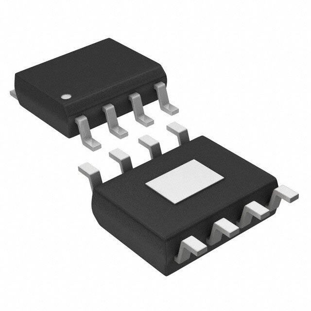
ICGOO电子元器件商城为您提供ADN4661BRZ由Analog设计生产,在icgoo商城现货销售,并且可以通过原厂、代理商等渠道进行代购。 ADN4661BRZ价格参考¥6.20-¥14.99。AnalogADN4661BRZ封装/规格:接口 - 驱动器,接收器,收发器, 驱动器 1/0 LVDS 8-SOIC。您可以下载ADN4661BRZ参考资料、Datasheet数据手册功能说明书,资料中有ADN4661BRZ 详细功能的应用电路图电压和使用方法及教程。
ADN4661BRZ 是由 Analog Devices Inc.(ADI)生产的一款高性能接口芯片,属于驱动器、接收器、收发器类别。其应用场景主要包括以下方面:

1. 工业自动化:
   ADN4661BRZ 适用于工业控制和自动化系统中的数据通信。它支持高速信号传输,能够在复杂的工业环境中提供可靠的数据交换,例如用于可编程逻辑控制器(PLC)、分布式控制系统(DCS)以及传感器与执行器之间的通信。

2. 医疗设备:
   在医疗领域,该器件可用于需要高精度和低延迟的设备中,如超声波设备、患者监护仪或诊断仪器。其稳定性和抗干扰能力确保了关键数据的准确传输。

3. 通信基础设施:
   ADN4661BRZ 可应用于电信网络中的信号处理部分,例如光纤通信模块、基站接口或路由器设计中。它能够满足这些应用对带宽和可靠性的严格要求。

4. 汽车电子:
   在现代汽车中,这款芯片可以用于车载网络系统,比如 CAN 总线或其他高速通信协议。它的耐久性和适应恶劣环境的能力使其非常适合汽车行业的严苛标准。

5. 测试与测量设备:
   对于需要快速响应和高精度的测试仪器(如示波器、信号发生器等),ADN4661BRZ 提供了理想的解决方案,帮助实现高效的数据采集和分析功能。

总之,ADN4661BRZ 凭借其卓越的性能参数(如低功耗、高数据速率和强大的 EMC 性能),成为众多高科技领域的理想选择。具体应用时需结合实际需求进行详细评估和设计匹配。
| 参数 | 数值 |
| 产品目录 | 集成电路 (IC)半导体 |
| 描述 | IC DRIVER DIFF LVDS 1CH 8SOICLVDS 接口集成电路 SGL 3V CMOS High Spd Diff Dvr |
| 产品分类 | |
| 品牌 | Analog Devices Inc |
| 产品手册 | |
| 产品图片 |
|
| rohs | 符合RoHS无铅 / 符合限制有害物质指令(RoHS)规范要求 |
| 产品系列 | 接口 IC,LVDS 接口集成电路,Analog Devices ADN4661BRZ- |
| 数据手册 | |
| 产品型号 | ADN4661BRZ |
| 产品目录页面 | |
| 产品种类 | LVDS 接口集成电路 |
| 传播延迟时间 | 1.5 ns |
| 供应商器件封装 | 8-SOIC |
| 包装 | 管件 |
| 协议 | LVDS |
| 双工 | - |
| 商标 | Analog Devices |
| 安装类型 | 表面贴装 |
| 安装风格 | SMD/SMT |
| 封装 | Tube |
| 封装/外壳 | 8-SOIC(0.154",3.90mm 宽) |
| 封装/箱体 | SOIC-8 |
| 工作温度 | -40°C ~ 85°C |
| 工作电源电压 | 3.3 V |
| 工厂包装数量 | 98 |
| 接收器滞后 | - |
| 接收机数量 | 1 |
| 数据速率 | 600Mbps |
| 最大工作温度 | + 85 C |
| 最小工作温度 | - 40 C |
| 标准包装 | 98 |
| 激励器数量 | 1 |
| 电压-电源 | 3 V ~ 3.6 V |
| 电源电压-最大 | 3.6 V |
| 电源电压-最小 | 3 V |
| 类型 | 驱动器 |
| 系列 | ADN4661 |
| 驱动器/接收器数 | 1/0 |


- 商务部:美国ITC正式对集成电路等产品启动337调查
- 曝三星4nm工艺存在良率问题 高通将骁龙8 Gen1或转产台积电
- 太阳诱电将投资9.5亿元在常州建新厂生产MLCC 预计2023年完工
- 英特尔发布欧洲新工厂建设计划 深化IDM 2.0 战略
- 台积电先进制程称霸业界 有大客户加持明年业绩稳了
- 达到5530亿美元!SIA预计今年全球半导体销售额将创下新高
- 英特尔拟将自动驾驶子公司Mobileye上市 估值或超500亿美元
- 三星加码芯片和SET,合并消费电子和移动部门,撤换高东真等 CEO
- 三星电子宣布重大人事变动 还合并消费电子和移动部门
- 海关总署:前11个月进口集成电路产品价值2.52万亿元 增长14.8%


PDF Datasheet 数据手册内容提取
Single, 3 V, CMOS, LVDS, High Speed Differential Driver ADN4661 FEATURES FUNCTIONAL BLOCK DIAGRAM ±15 kV ESD protection on output pins VCC 600 Mbps (300 MHz) switching rates ADN4661 Flow-through pinout simplifies PCB layout DOUT+ 300 ps typical differential skew DIN 700 ps maximum differential skew DOUT– 1.5 ns maximum propagation delay 3±.335 V5 pmoVw deirf fseurpepnltyia l signaling NC = NON CCOGNNNDECNTC NC 07876-001 Low power dissipation: 23 mW typical Figure 1. Interoperable with existing 5 V LVDS receivers Conforms to TIA/EIA-644 LVDS standards Industrial operating temperature range (−40°C to +85°C) Available in surface-mount (SOIC) package APPLICATIONS Backplane data transmission Cable data transmission Clock distribution GENERAL DESCRIPTION The ADN4661 is a single, CMOS, low voltage differential The ADN4661 and a companion LVDS receiver offer a new signaling (LVDS) line driver offering data rates of over solution to high speed point-to-point data transmission, and a 600 Mbps (300 MHz) and ultra-low power consumption. low power alternative to emitter-coupled logic (ECL) or positive It features a flow-through pinout for easy PCB layout and emitter-coupled logic (PECL). separation of input and output signals. The device accepts low voltage TTL/CMOS logic signals and converts them to a differential current output of typically ±3.1 mA for driving a transmission medium such as a twisted- pair cable. The transmitted signal develops a differential voltage of typically ±355 mV across a termination resistor at the receiv- ing end, and this is converted back to a TTL/CMOS logic level by a line receiver. Rev. 0 Information furnished by Analog Devices is believed to be accurate and reliable. However, no responsibility is assumed by Analog Devices for its use, nor for any infringements of patents or other One Technology Way, P.O. Box 9106, Norwood, MA 02062-9106, U.S.A. rights of third parties that may result from its use. Specifications subject to change without notice. No license is granted by implication or otherwise under any patent or patent rights of Analog Devices. Tel: 781.329.4700 www.analog.com Trademarks and registered trademarks are the property of their respective owners. Fax: 781.461.3113 ©2008 Analog Devices, Inc. All rights reserved.
ADN4661 TABLE OF CONTENTS Features .............................................................................................. 1 ESD Caution...................................................................................5 Applications ....................................................................................... 1 Pin Configuration and Function Descriptions ..............................6 Functional Block Diagram .............................................................. 1 Typical Performance Characteristics ..............................................7 General Description ......................................................................... 1 Theory of Operation ...................................................................... 10 Revision History ............................................................................... 2 Applications Information .......................................................... 10 Specifications ..................................................................................... 3 Outline Dimensions ....................................................................... 11 AC Characteristics ........................................................................ 4 Ordering Guide .......................................................................... 11 Absolute Maximum Ratings ............................................................ 5 REVISION HISTORY 12/08—Revision 0: Initial Version Rev. 0 | Page 2 of 12
ADN4661 SPECIFICATIONS V = 3 V to 3.6 V; R = 100 Ω; C = 15 pF to GND; all specifications T to T , unless otherwise noted. CC L L MIN MAX Table 1. Parameter1, 2 Symbol Min Typ Max Unit Test Conditions LVDS OUTPUTS (D , D ) OUT+ OUT− Differential Output Voltage V 250 355 450 mV See Figure 2 and Figure 4 OD Change in Magnitude of V for Complementary ΔV 1 35 |mV| See Figure 2 and Figure 4 OD OD Output States Offset Voltage V 1.125 1.2 1.375 V See Figure 2 and Figure 4 OS Change in Magnitude of V for Complementary ΔV 3 25 |mV| See Figure 2 and Figure 4 OS OS Output States Output High Voltage V 1.4 1.6 V See Figure 2 and Figure 4 OH Output Low Voltage V 0.90 1.1 V See Figure 2 and Figure 4 OL INPUTS (D , V ) IN CC Input High Voltage V 2.0 VCC V IH Input Low Voltage V GND 0.8 V IL Input High Current I −10 ±2 +10 μA V = 3.3 V or 2.4 V IH IN Input Low Current I −10 ±1 +10 μA V = GND or 0.5 V IL IN Input Clamp Voltage V −1.5 −0.6 V I = −18 mA CL CL LVDS OUTPUT PROTECTION (D , D ) OUT+ OUT− Output Short-Circuit Current3 I −5.7 −8.0 mA D = V , D = 0 V or D = GND, D = 0 V OS IN CC OUT+ IN OUT− LVDS OUTPUT LEAKAGE (D , D ) OUT+ OUT− Power-Off Leakage I −10 ±1 +10 μA V = V or GND, V = 0 V OFF OUT CC CC POWER SUPPLY Supply Current, Unloaded I 4.0 8.0 mA No load, D = V or GND CC IN CC Supply Current, Loaded I 7 10 mA D = V or GND CCL IN CC ESD PROTECTION D , D Pins ±15 kV Human body model OUT+ OUT− All Pins Except D , D ±4 kV Human body model OUT+ OUT− 1 Current into device pins is defined as positive. Current out of device pins is defined as negative. All voltages are referenced to ground except VOD, ΔVOD, and ΔVOS. 2 The ADN4661 is a current mode device and functions within data sheet specifications only when a resistive load is applied to the driver outputs. Typical range is 90 Ω to 110 Ω. 3 Output short-circuit current (IOS) is specified as magnitude only; minus sign indicates direction only. Rev. 0 | Page 3 of 12
ADN4661 AC CHARACTERISTICS V = 3 V to 3.6 V; R = 100 Ω; C 1 = 15 pF to GND; all specifications T to T , unless otherwise noted. CC L L MIN MAX Table 2. Parameter2 Symbol Min Typ Max Unit Conditions/Comments3, 4 Differential Propagation Delay High to Low t 0.3 0.8 1.5 ns See Figure 3 and Figure 4 PHLD Differential Propagation Delay Low to High t 0.3 1.1 1.5 ns See Figure 3 and Figure 4 PLHD Differential Pulse Skew |t − t |5 t 0 0.3 0.7 ns See Figure 3 and Figure 4 PHLD PLHD SKD1 Differential Part-to-Part Skew6 t 0 1.0 ns See Figure 3 and Figure 4 SKD3 Differential Part-to-Part Skew7 t 0 1.2 Ns See Figure 3 and Figure 4 SKD4 Rise Time t 0.2 0.5 1.0 ns See Figure 3 and Figure 4 TLH Fall Time t 0.2 0.5 1.0 ns See Figure 3 and Figure 4 THL Maximum Operating Frequency8 f 350 MHz See Figure 3 MAX 1 CL includes probe and jig capacitance. 2 AC parameters are guaranteed by design and characterization. 3 Generator waveform for all tests, unless otherwise specified: f = 50 MHz, ZO = 50 Ω, tTLH ≤ 1 ns, and tTHL ≤ 1 ns. 4 All input voltages are for one channel unless otherwise specified. Other inputs are set to GND. 5 tSKD1 = |tPHLD − tPLHD| is the magnitude difference in differential propagation delay time between the positive going edge and the negative going edge of the same channel. 6 tSKD3, differential part-to-part skew, is defined as the difference between the minimum and maximum specified differential propagation delays. This specification applies to devices at the same VCC and within 5°C of each other within the operating temperature range. 7 tSKD4, differential part-to-part skew, is the differential channel-to-channel skew of any event between devices. This specification applies to devices over recommended operating temperatures and voltage ranges, and across process distribution. tSKD4 is defined as |maximum − minimum| differential propagation delay. 8 fMAX generator input conditions: tTLH = tTHL < 1 ns (0% to 100%), 50% duty cycle, 0 V to 3 V. Output criteria: duty cycle = 45% to 55%, VOD > 250 mV, all channels switching. Test Circuits and Timing Diagrams DOUT+ VCC VCC RL/2 DIN RL/2 V VOS V VOD DOUT– 07876-002 Figure 2. Test Circuit for Driver VOD and VOS VCC DOUT+ CL SIGNAL DIN GENERATOR 50Ω DOUT– CL N1.O CTLE ISNCLUDES PROBE AND JIG CAPACITANCE. 07876-003 Figure 3. Test Circuit for Driver Propagation Delay, Transition Time, and Maximum Operating Frequency 3V DIN 1.5V 0V t t PLHD VOD PHLD DOUT– VOH 0V (DIFFERENTIAL) DOUT+ VOL 80% VDIFF 0V 20% VDIFF = DOUT+–DOUT– tTLH tTHL 07876-004 Figure 4. Driver Propagation Delay and Transition Time Waveforms Rev. 0 | Page 4 of 12
ADN4661 ABSOLUTE MAXIMUM RATINGS T = 25°C, unless otherwise noted. All voltages are relative to Stresses above those listed under Absolute Maximum Ratings A their respective ground. may cause permanent damage to the device. This is a stress rating only; functional operation of the device at these or any Table 3. other conditions above those indicated in the operational Parameter Rating section of this specification is not implied. Exposure to absolute VCC to GND −0.3 V to +4 V maximum rating conditions for extended periods may affect Input Voltage (DIN) to GND −0.3 V to VCC + 0.3 V device reliability. Output Voltage (D , D ) to GND −0.3 V to V + 0.3 V OUT+ OUT− CC Short-Circuit Duration (D , D ) to GND Continuous OUT+ OUT− Operating Temperature Range ESD CAUTION Industrial −40°C to +85°C Storage Temperature Range −65°C to +150°C Junction Temperature (T max) 150°C J Power Dissipation (T max − T )/θ J A JA SOIC Package θ Thermal Impedance 149.5°C/W JA Reflow Soldering Peak Temperature Pb-Free 260°C ± 5°C Rev. 0 | Page 5 of 12
ADN4661 PIN CONFIGURATION AND FUNCTION DESCRIPTIONS VCC 1 8 DOUT– DIN 2 ADN4661 7 DOUT+ NC 3 TOP VIEW 6 NC GND N4C (=N oNtO to C SOcNaNleE)CT5 NC 07876-005 Figure 5. Pin Configuration Table 4. Pin Function Descriptions Pin No. Mnemonic Description 1 V Power Supply Input. The part can be operated from 3.0 V to 3.6 V, and the supply should be decoupled with a CC 10 μF solid tantalum capacitor in parallel with a 0.1 μF capacitor to GND. 2 D Driver Logic Input. IN 3 NC No Connect. This pin should be left unconnected. 4 GND Ground. Reference point for all circuitry on the part. 5 NC No Connect. This pin should be left unconnected. 6 NC No Connect. This pin should be left unconnected. 7 D Noninverting Output Current Driver. When D is high, current flows out of D . When D is low, current flows into D . OUT+ IN OUT+ IN OUT+ 8 D Inverting Output Current Driver. When D is high, current flows into D . When D is low, current flows out of D . OUT− IN OUT− IN OUT− Rev. 0 | Page 6 of 12
ADN4661 TYPICAL PERFORMANCE CHARACTERISTICS 1.415 325.0 TRAL == 2150°0CΩ mV) TRAL == 2150°0CΩ (V)OH E, V (OD 324.8 V G AGE, 1.414 OLTA 324.6 T V H VOL TPUT G U 324.4 PUT HI 1.413 TIAL O T N OU RE 324.2 E F F DI 1.4123.0 3.1 POWE3R.2 SUPPLY3 V.3OLTAGE3,. 4VCC (V) 3.5 3.6 07876-006 324.03.0 3.1 POWE3R.2 SUPPLY3 V.3OLTAGE3,. 4VCC (V) 3.5 3.6 07876-009 Figure 6. Output High Voltage vs. Power Supply Voltage Figure 9. Differential Output Voltage vs. Power Supply Voltage 1.090 500 TRAL == 2150°0CΩ mV) TVAC C= =2 53°.3CV V (V)OL GE, V (OD 450 AGE, 1.089 OLTA 400 T V W VOL TPUT UT LO 1.088 AL OU 350 P TI T N OU RE 300 E F F DI 1.0873.0 3.1 POWE3R.2 SUPPLY3 V.3OLTAGE3,. 4VCC (V) 3.5 3.6 07876-007 25090 100 L11O0AD RES1IS20TOR, RL1 (3Ω0) 140 150 07876-010 Figure 7. Output Low Voltage vs. Power Supply Voltage Figure 10. Differential Output Voltage vs. Load Resistor –3.9 1.252 VIN = GNDTA O =R 2 V5C°CC TRAL == 2150°0CΩ A) VOUT = 0V m (OS mV) NT, I –4.0 V (OS 1.251 RE E, R G U A C T UIT VOL CIRC –4.1 SET 1.250 ORT- OFF H S –4.23.0 3.1 POWE3R.2 SUPPLY3 V.3OLTAGE3,. 4VCC (V) 3.5 3.6 07876-008 1.2493.0 3.1 POWE3R.2 SUPPLY3 V.3OLTAGE3,. 4VCC (V) 3.5 3.6 07876-011 Figure 8. Output Short-Circuit Current vs. Power Supply Voltage Figure 11. Offset Voltage vs. Power Supply Voltage Rev. 0 | Page 7 of 12
ADN4661 1200 UPPLY CURRENT, I (mA)CC 1111197531 VTVRCACILLN C ==== =2 110 5503V°p0.3CΩFTVO 3V AL PROPAGATION DELAY (ns) 11010000 tPLHD tPHLD TfCR A=LL 1===M 211H550°p0zCΩF R S 9 NTI E E W R O FE P 7 F DI 05.01 0.1 SWITCHIN1G FREQUE1N0CY (MHz) 100 1k07876-012 9003.0 3.1 POWE3R.2 SUPPLY3 V.3OLTAGE3,. 4VCC (V) 3.5 3.607876-015 Figure 12. Power Supply Current vs. Switching Frequency Figure 15. Differential Propagation Delay vs. Power Supply Voltage 10.0 1200 TA = 25°C s) Vf C=C 1 =M 3H.z3V mA) 9.5 fV =IN 1=M 0HVzTO 3V AY (n CRLL == 1150p0ΩF ENT, I (CC 9.0 CRLL == 1150p0ΩF TION DEL 1100 tPLHD R 8.5 A R G U A C P LY 8.0 RO tPHLD P P UP AL 1000 R S 7.5 NTI E E W R PO 7.0 FFE DI 6.53.0 POWER SUPPLY3 V.3OLTAGE, VCC (V) 3.607876-013 900–40 –20 AM0BIENT TE20MPERAT40URE, TA6 (0°C) 80 100 07876-016 Figure 13. Power Supply Current vs. Power Supply Voltage Figure 16. Differential Propagation Delay vs. Ambient Temperature 9 100 VCC = 3.3V TA = 25°C f = 1MHz f = 1MHz ENT, I (mA)CC 8 RCVILLN === 11050Vp0ΩF W, t (ps)SKD1 6800 CRLL == 1150p0ΩF PLY CURR 7 TIAL SKE 40 P N U E S R WER 6 DIFFE 20 O P 5–40 –15AMBIENT 1T0EMPERATU3R5E, TA (°C)60 8507876-014 03.0 3.1 POWE3R.2 SUPPLY3 V.3OLTAGE3,. 4VCC (V) 3.5 3.6 07876-017 Figure 14. Power Supply Current vs. Ambient Temperature Figure 17. Differential Skew vs. Power Supply Voltage Rev. 0 | Page 8 of 12
ADN4661 50 400 VCC = 3.3V VCC = 3.3V f = 1MHz f = 1MHz CL = 15pF CL = 15pF s) 40 RL = 100Ω RL = 100Ω p (D1 s) 380 K p W, tS 30 ME ( tTLH E TI NTIAL SK 20 NSITION 360 tTHL E A R R E T F 340 DIF 10 0–40 –20 AM0BIENT TE20MPERAT40URE, TA6 (0°C) 80 100 07876-018 320–40 –20 AM0BIENT TE20MPERAT40URE, TA6 (0°C) 80 100 07876-020 Figure 18. Differential Skew vs. Ambient Temperature Figure 20. Transition Time vs. Ambient Temperature 400 TA = 25°C f = 1MHz CL = 15pF RL = 100Ω 380 ps) tTLH E ( M TI TION 360 tTHL SI N A R T 340 3203.0 3.1 POWE3R.2 SUPPLY3 V.3OLTAGE3,. 4VCC (V) 3.5 3.6 07876-019 Figure 19. Transition Time vs. Power Supply Voltage Rev. 0 | Page 9 of 12
ADN4661 THEORY OF OPERATION The ADN4661 is a single line driver for low voltage differential A current-mode device simply reverses a constant current signaling. It takes a single-ended 3 V logic signal and converts between its two outputs, with no significant overlap currents. it to a differential current output. The data can then be trans- This is similar to emitter-coupled logic (ECL) and positive mitted for considerable distances, over media such as a twisted- emitter-coupled logic (PECL), but without the high quiescent pair cable or PCB backplane, to an LVDS receiver, where it current of ECL and PECL. develops a voltage across a terminating resistor, R . This resistor T is chosen to match the characteristic impedance of the medium, APPLICATIONS INFORMATION typically around 100 Ω. The differential voltage is detected by Figure 21 shows a typical application for point-to-point data the receiver and converted back into a single-ended logic signal. transmission using the ADN4661 as the driver and the LVDS When D is high (Logic 1), current flows out of the D pin IN OUT+ receiver. (current source) through R and back to the D pin (current T OUT− +3.3V +3.3V sink). At the receiver, this current develops a positive differential 0.1µF +10µF 0.1µF +10µF TANTALUM TANTALUM voltage across R (with respect to the inverting input) and results T VCC VCC in a Logic 1 at the receiver output. When D is low (Logic 0), D sinks current and D sources currentIN. A negative differen- ADN4661 DOUT+ DIN+ LVDS RECEIVER OUT+ OUT− tial voltage across RT results in a Logic 0 at the receiver output. DIN DOURT–T 10D0IΩN– DOUT T(thype iocualtlpyu ±t 3d.5ri5v me cAu)r, rdeenvte ilso pbientgw beeetnw ±ee2n.5 ± m25A0 amnVd ±an4d.5 ± m45A0 mV GND GND 07876-021 across a 100 Ω termination resistor. The received voltage is centered Figure 21. Typical Application Circuit around the receiver offset of 1.2 V. Therefore, the noninverting receiver input for Logic 1 is typically (1.2 V + [355 mV/2]) = 1.377 V, and the inverting receiver input is (1.2 V − [355 mV/2]) = 1.023 V. For Logic 0, the inverting and noninverting output voltages are reversed. Note that because the differential voltage reverses polarity, the peak-to-peak voltage swing across R is T twice the differential voltage. Current-mode drivers offer considerable advantages over voltage mode drivers such as RS-422 drivers. The operating current remains fairly constant with increased switching frequency, whereas the current of voltage mode drivers increases exponentially in most cases. This is caused by the overlap as internal gates switch between high and low, which causes currents to flow from the device power supply to ground. Rev. 0 | Page 10 of 12
ADN4661 OUTLINE DIMENSIONS 5.00(0.1968) 4.80(0.1890) 8 5 4.00 (0.1574) 6.20 (0.2441) 3.80 (0.1497) 1 4 5.80 (0.2284) 1.27 (0.0500) 0.50 (0.0196) 45° BSC 1.75 (0.0688) 0.25 (0.0099) 0.25 (0.0098) 1.35 (0.0532) 8° 0.10 (0.0040) 0° COPLANARITY 0.51 (0.0201) 1.27 (0.0500) 0.10 SEATING 0.31 (0.0122) 0.25 (0.0098) 0.40 (0.0157) PLANE 0.17 (0.0067) COMPLIANTTO JEDEC STANDARDS MS-012-AA CONTROLLING DIMENSIONSARE IN MILLIMETERS; INCH DIMENSIONS A (RINEFPEARREENNCTEH EOSNELSY)AANRDE ARROEU NNODETDA-POPFRFO MPIRLLIAIMTEE TFEORR EUQSUEI VINA LDEENSTIGS NF.OR 012407- Figure 22. 8-Lead Standard Small Outline Package [SOIC_N] Narrow Body (R-8) Dimensions shown in millimeters and (inches) ORDERING GUIDE Model Temperature Range Package Description Package Option ADN4661BRZ1 −40°C to +85°C 8-Lead Standard Small Outline Package [SOIC-N] R-8 ADN4661BRZ-REEL71 −40°C to +85°C 8-Lead Standard Small Outline Package [SOIC-N] R-8 1 Z = RoHS Compliant Part. Rev. 0 | Page 11 of 12
ADN4661 NOTES ©2008 Analog Devices, Inc. All rights reserved. Trademarks and registered trademarks are the property of their respective owners. D07876-0-12/08(0) Rev. 0 | Page 12 of 12
Mouser Electronics Authorized Distributor Click to View Pricing, Inventory, Delivery & Lifecycle Information: A nalog Devices Inc.: ADN4661BRZ ADN4661BRZ-REEL7

 Datasheet下载
