ICGOO在线商城 > 集成电路(IC) > PMIC - 监控器 > ADM8710L2ARJZ-RL7
 Datasheet下载
- 型号: ADM8710L2ARJZ-RL7
- 制造商: Analog
- 库位|库存: xxxx|xxxx
- 要求:
| 数量阶梯 | 香港交货 | 国内含税 |
| +xxxx | $xxxx | ¥xxxx |
查看当月历史价格
查看今年历史价格
ADM8710L2ARJZ-RL7产品简介:
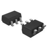
ICGOO电子元器件商城为您提供ADM8710L2ARJZ-RL7由Analog设计生产,在icgoo商城现货销售,并且可以通过原厂、代理商等渠道进行代购。 ADM8710L2ARJZ-RL7价格参考。AnalogADM8710L2ARJZ-RL7封装/规格:PMIC - 监控器, 开路漏极或开路集电极 监控器 4 通道 SOT-23-6。您可以下载ADM8710L2ARJZ-RL7参考资料、Datasheet数据手册功能说明书,资料中有ADM8710L2ARJZ-RL7 详细功能的应用电路图电压和使用方法及教程。
| 参数 | 数值 |
| 产品目录 | 集成电路 (IC) |
| 描述 | IC SUPERVISOR QUAD SOT23-6 |
| 产品分类 | |
| 品牌 | Analog Devices Inc |
| 数据手册 | |
| 产品图片 |
|
| 产品型号 | ADM8710L2ARJZ-RL7 |
| rohs | 无铅 / 符合限制有害物质指令(RoHS)规范要求 |
| 产品系列 | - |
| 供应商器件封装 | SOT-23-6 |
| 其它名称 | ADM8710L2ARJZ-RL7DKR |
| 包装 | Digi-Reel® |
| 受监控电压数 | 4 |
| 复位 | 低有效 |
| 复位超时 | 最小为 35 ms |
| 安装类型 | 表面贴装 |
| 封装/外壳 | SOT-23-6 |
| 工作温度 | -40°C ~ 85°C |
| 标准包装 | 1 |
| 电压-阈值 | 1.73V,3.07V,可调,可调 |
| 类型 | 多压监控器 |
| 输出 | 开路漏极或开路集电极 |


- 商务部:美国ITC正式对集成电路等产品启动337调查
- 曝三星4nm工艺存在良率问题 高通将骁龙8 Gen1或转产台积电
- 太阳诱电将投资9.5亿元在常州建新厂生产MLCC 预计2023年完工
- 英特尔发布欧洲新工厂建设计划 深化IDM 2.0 战略
- 台积电先进制程称霸业界 有大客户加持明年业绩稳了
- 达到5530亿美元!SIA预计今年全球半导体销售额将创下新高
- 英特尔拟将自动驾驶子公司Mobileye上市 估值或超500亿美元
- 三星加码芯片和SET,合并消费电子和移动部门,撤换高东真等 CEO
- 三星电子宣布重大人事变动 还合并消费电子和移动部门
- 海关总署:前11个月进口集成电路产品价值2.52万亿元 增长14.8%


PDF Datasheet 数据手册内容提取
Low Voltage, High Accuracy, Quad Voltage Microprocessor Supervisory Circuit Data Sheet ADM8710 FEATURES FUNCTIONAL BLOCK DIAGRAM Accurate monitoring of up to four power supply voltages IN1 2 factory-set threshold options for monitoring 1.8 V and 3.3 V ADM8710 Adjustable input threshold voltage 0.62 V (±1.5% accuracy) IN2 50 ms typical reset timeout IN2 Open-drain RESET output (10 µA internal pull-up) RESET Reset output stage: active low, valid to IN1 = 1 V or IN2 = 1 V RESET Power supply glitch immunity TIMEOUT Specified from −40°C to +85°C IN3 UVLO 6-lead SOT-23 package APPLICATIONS IN4 Telecommunications MDeicsrkotporpo acnesds noor tseybstoeomks c omputers 0.62VREF 10647-001 Figure 1. Data storage equipment Servers/workstations GENERAL DESCRIPTION The ADM8710 is a low voltage, high accuracy supervisory circuit. If a monitored power supply voltage falls below the minimum The device monitors up to four system supply voltages. voltage threshold, a single active low output asserts, triggering a system reset. The output is open drain with a weak internal The ADM8710 incorporates two internally pretrimmed under- pull-up to the monitored IN supply of typically 10 µA. When voltage threshold options for monitoring 1.8 V and 3.3 V supply 2 all voltages rise above the selected threshold level, the RESET voltages. It also offers two adjustable inputs with 0.62 V internal signal remains low for the reset timeout period. The ADM8710 reference, allowing users to program the reset threshold through output remains valid as long as IN or IN exceeds 1 V. external resistor dividers. The combination of pretrimmed and 1 2 adjustable inputs gives the ADM8710 the advantage of being Unused monitored inputs should not be allowed to float or to both space saving and flexible. be grounded. Instead, connect them to a supply voltage greater than their specified threshold voltages. The ADM8710 is available in a 6-lead SOT-23 package. The device operates over the extended temperature range of −40°C to +85°C. Rev. 0 Information furnished by Analog Devices is believed to be accurate and reliable. However, no responsibility is assumed by Analog Devices for its use, nor for any infringements of patents or other One Technology Way, P.O. Box 9106, Norwood, MA 02062-9106, U.S.A. rights of third parties that may result from its use. Specifications subject to change without notice. No license is granted by implication or otherwise under any patent or patent rights of Analog Devices. Tel: 781.329.4700 www.analog.com Trademarks and registered trademarks are the property of their respective owners. Fax: 781.461.3113 ©2012 Analog Devices, Inc. All rights reserved.
ADM8710 Data Sheet TABLE OF CONTENTS Features .............................................................................................. 1 Theory of Operation .........................................................................8 Applications ....................................................................................... 1 Input Configuration ......................................................................8 Functional Block Diagram .............................................................. 1 RESET Output Configuration .....................................................8 General Description ......................................................................... 1 Addition of Manual Reset ............................................................8 Revision History ............................................................................... 2 Tolerance and Accuracy ...............................................................9 Specifications ..................................................................................... 3 Model Options ................................................................................ 10 Absolute Maximum Ratings ............................................................ 4 Outline Dimensions ....................................................................... 11 ESD Caution .................................................................................. 4 Ordering Guide .......................................................................... 11 Pin Configuration and Function Descriptions ............................. 5 Typical Performance Characteristics ............................................. 6 REVISION HISTORY 8/12—Revision 0: Initial Version Rev. 0 | Page 2 of 12
Data Sheet ADM8710 SPECIFICATIONS V = 1 V to 5.5 V, T = −40°C to +85°C, unless otherwise noted. Typical values are V = 3.0 V to 3.3 V, T = 25°C. IN2 A IN2 A Table 1. Parameter Min Typ Max Units Test Conditions/Comments OPERATING VOLTAGE RANGE V 1 1.0 5.5 V T = 0°C to 85°C IN2 A 1.2 5.5 V T = −40°C to +85°C A INPUT CURRENT IN Input Current 55 115 µA IN = nominal input voltage (3.3 V supplies); x 2 the supply splits into 25 µA for the resistor divider and 30 µA for other circuits 25 40 µA IN = nominal input voltage (1.8 V supplies) 3 0.4 µA V = 0 V to 0.85 V IN1 0.2 µA V = 0 V to 0.85 V IN4 THRESHOLD VOLTAGE Threshold Voltage (V ) 3.010 3.07 3.130 V IN decreasing; 3.3 V (−5% supply tolerance) TH X 1.705 1.73 1.760 V IN decreasing; 1.8 V (−2% supply tolerance) X Adjustable Input Threshold Voltage (V ) 0.611 0.62 0.629 V IN decreasing TH X RESET Reset Threshold Hysteresis (V ) 0.3 %V IN increasing relative to IN decreasing HYST TH X X Reset Threshold Temperature Coefficient (TCV ) 60 ppm/°C TH IN to Reset Delay (t ) 30 µs V falling at 10 mV/µs from V to V − 50 mV X RP IN TH TH Reset Timeout Period (t ) 35 50 70 ms RP RESET Output Low (V ) 0.3 V V = 5 V, I = 2 mA OL IN2 SINK 0.4 V V = 2.5 V, I = 1.2 mA IN2 SINK 0.3 V V = 1.0 , I = 20 µA, T = 0°C to +85°C IN2 SINK A RESET Output High (V ) 0.8 × V V V ≥ 2.0 V, I = 4 µA, RESET deasserted OH IN2 IN2 SOURCE RESET Output High Source Current (I ) 10 µA V ≥ 2.0 V, RESET deasserted OH IN2 1 The RESET output is guaranteed to be in the correct state for IN or IN down to 1 V. 1 2 Rev. 0 | Page 3 of 12
ADM8710 Data Sheet ABSOLUTE MAXIMUM RATINGS Table 3. Thermal Resistance Table 2. Package Type θ Unit Parameter Rating JA 6-lead SOT-23 169.5 °C/W IN , RESET to GND −0.3 V to +6 V X Continuous RESET Current 20 mA Storage Temperature Range −65°C to +125°C ESD CAUTION Operating Temperature Range −40°C to +85°C Lead Temperature (10 sec) 300°C Junction Temperature 135°C Stresses above those listed under Absolute Maximum Ratings may cause permanent damage to the device. This is a stress rating only; functional operation of the device at these or any other conditions above those indicated in the operational section of this specification is not implied. Exposure to absolute maximum rating conditions for extended periods may affect device reliability. Rev. 0 | Page 4 of 12
Data Sheet ADM8710 PIN CONFIGURATION AND FUNCTION DESCRIPTIONS IN1 1 6 RESET ADM8710 IN2 2 TOP VIEW 5 GND (Not to Scale) IN3 3 4 IN4 10647-002 Figure 2. Pin Configuration Table 4. Pin Function Descriptions Pin No. Mnemonic Description 1 IN Input Voltage 1. 1 2 IN Input Voltage 2. 2 3 IN Input Voltage 3. 3 4 IN Input Voltage 4. 4 5 GND Ground. 6 RESET Active Low RESET Output. RESET goes low when an input drops to less than the specified threshold. When all inputs rise higher than the threshold voltage, RESET remains low for the reset timeout period before going high. RESET is open drain with a weak internal pull-up to IN. 2 Rev. 0 | Page 5 of 12
ADM8710 Data Sheet TYPICAL PERFORMANCE CHARACTERISTICS V = 3.0 V, T = 25°C, unless otherwise noted. IN2 A 60 100 58 s) 90 µ N ( 56 O 80 A) ATI µ 54 R 70 ENT ( 52 T DU 60 R N R E U 50 SI 50 C N PUT 48 TRA 40 N X IN I2 46 UM IN 30 RESET ASSERTED ABOVE THIS LINE 44 M 20 XI 4420 VVIINN22 == 33.V3V 10647-003 MA 100 10647-006 –40 –15 10 35 60 85 0 100 200 300 400 500 600 700 800 900 1000 TEMPERATURE (ºC) RESET THRESHOLD OVERDRIVE (mV) Figure 3. IN Input Current vs. Temperature Figure 6. Maximum IN Transient Duration vs. Reset Threshold Overdrive 2 x 120 100 90 100 80 A) ENT (µ 80 Y (µs) 7600 R A R L CU 60 DE 50 T T PU SE 40 N IN2 40 RE 30 I 20 20 0 10647-004 100 10647-007 0 0.5 1.0 1.5 2.0 2.5 3.0 3.5 4.0 4.5 5.0 5.5 0 100 200 300 400 500 600 700 800 900 1000 IN2 VOLTAGE (V) RESET THRESHOLD OVERDRIVE (mV) Figure 4. IN Input Current vs. IN Voltage Figure 7. RESET Delay vs. Reset Threshold Overdrive (IN Decreasing) 2 2 x 0.05 59.0 %) 0 58.5 ROR (–0.05 ms)58.0 LD ER–0.10 ELAY (57.5 O D RSH–0.15 OUT 57.0 ED THE–0.20 T TIME56.5 Z E MALI–0.25 RES56.0 R O N––00..3305 VVTINH2 == 13..83VV 10647-005 5555..05 –40 –15 TE1M0PERATURE3 5(ºC) 60 85 –40 –15 TE1M0PERATURE3 5(°C) 60 85 10647-008 Figure 5. Normalized Threshold Error vs. Temperature Figure 8. Normalized Reset Timeout Delay vs. Temperature Rev. 0 | Page 6 of 12
Data Sheet ADM8710 INx INx 1 1 RESET RESET 2 10647-009 2 10647-010 CH3 2.0V M10.0µs 125MS/s A CH3 960mV CH3 2.0V M10.0ms 125kS/s A CH3 960mV CH4 2.0V 8.0ns/pt CH4 2.0V 8.0µs/pt Figure 9. RESET Pull-Up and Pull-Down Response (10 µs/DIV) Figure 10. Timeout Delay (10 ms/DIV) Rev. 0 | Page 7 of 12
ADM8710 Data Sheet THEORY OF OPERATION Do not allow unused monitor inputs to float or to be grounded. The ADM8710 is a compact, low power supervisory circuit Connect these inputs to a supply voltage greater than their specified capable of monitoring up to four voltages in a multisupply threshold voltages. In the case of unused IN adjustable inputs, application. x limit the bias current by connecting a 1 MΩ series resistor between The device includes two factory-set voltage threshold options the unused input and IN. 2 for monitoring 1.8 V and 3.3 V supplies. It also provides two RESET OUTPUT CONFIGURATION adjustable thresholds for monitoring voltages down to 0.62 V. The ADM8710 is powered by IN2, which is a monitored voltage, The RESET output asserts low when a monitored INx voltage and therefore monitors up to four voltages. If a monitored voltage drops below its voltage threshold. When all voltages rise above drops below its associated threshold, the active low reset output the selected threshold level, the RESET signal remains low for asserts low and remains low while either IN or IN remains the reset timeout period. The RESET output is open drain with 1 2 above 1.0 V. a weak internal pull-up to the monitored IN, typically 10 µA. 2 1.2V Many applications that interface with other logic devices do not ADM8710 require an external pull-up resistor. However, if an external pull-up IN1 resistor is required and it is connected to a voltage ranging from 3.3V 1.8V IN2 RESET MICROPROCESSOR 0 V to 5.5 V, it overdrives the internal pull-up. Reverse current IN3 0.9V IN4 flow from the external pull-up voltage to IN2 is prevented by the internal circuitry. GND 10647-011 IN2 = 3.3V 5V Figure 11. Typical Applications Circuit VCC INPUT CONFIGURATION ADM8710 100kΩ The ADM8710 provides numerous monitor choices with RESET RESET adjustable reset thresholds. Typically, the threshold voltage at each adjustable IN input is 0.62 V. To monitor a voltage greater x tdheapnic 0te.6d2 i nV ,F ciognunree c1t2 a, wrehseisrteo r divider network to the circuit as 10647-013 Figure 13. Interface with a Different Logic Supply Voltage R1+R2 V =0.62V INTH R2 ADDITION OF MANUAL RESET VINTH Use the circuit shown in Figure 14 to add manual reset to any of the ADM8710 adjustable inputs. When the switch is closed, the R1 analog input shorts to ground and a RESET output commences. The switch must remain open for a minimum of 35 ms for R2 the RESET output to deassert. VREF = 0.62V 10647-012 ADM8710 Figure 12. Setting the Adjustable Monitor VIN4 IN1 IN2 The internal comparators each typically have a hysteresis of 0.3% R1 RESET IN3 with respect to the reset threshold. This built-in hysteresis IN4 improves the immunity of the device to ambient noise without GND noticeably reducing the threshold accuracy. The ADM8710 is R2 unaffected by short input transients. 10647-014 The ADM8710 is powered from the monitored IN. Monitored Figure 14. Addition of Manual Reset (IN is an Adjustable Input) 2 4 inputs are resistant to short power supply glitches. Figure 6 depicts the ADM8710 glitch immunity data. To increase noise immunity in noisy applications, place a 0.1 µF capacitor between the IN input 2 and ground. Adding capacitance to IN, IN, and IN also improves 1 3 4 noise immunity. Rev. 0 | Page 8 of 12
Data Sheet ADM8710 TOLERANCE AND ACCURACY The ADM8710 offers up to ±2% accuracy on factory trimmed monitoring thresholds and ±1.5% accuracy on adjustable The primary function of the voltage supervisor is to keep the thresholds over the entire operating temperature range. processor in a reset state whenever the processor supply voltage is below the specification limit. It needs to be able to differentiate the voltage out-of-processor limit from supply variations caused by voltage converter output tolerance. This means that the supervisor rest threshold should fit inside the narrow band between processor input tolerance and supply tolerance. VOLTAGE SUPPLY VOLTAGE SUPPLYTOLERANCE PROCESSOR INPUT TOLERANCE THRESHOLDTOLERANCE RESET tRP TIME 10647-015 Figure 15. Tighter Threshold Tolerance on Voltage Supervisor Reduces Accuracy Requirement on Monitored Supply Rev. 0 | Page 9 of 12
ADM8710 Data Sheet MODEL OPTIONS Table 5. Reset Voltage Threshold Options IN IN IN IN 1 2 3 4 Reset Nominal Nominal Nominal Nominal Threshold Input Supply Input Supply Input Supply Input Supply Code1 Voltage (V) Tolerance (%) Voltage (V) Tolerance (%) Voltage (V) Tolerance (%) Voltage (V) Tolerance (%) L Adjustable Not applicable 3.3 −5 1.8 −2 Adjustable Not applicable 1 Adjustable voltage based on 0.62 V internal threshold. The external threshold voltage can be set using an external resistor divider. Table 6. Reset Timeout Options T = −40°C to +85°C A Reset Timeout Period Code1 Min Typ Max Unit ADM8710x2 35 50 70 ms 1 x = do not care. ADM8710L2ARJZ-RL7 PACKING MATERIAL RESET THRESHOLD CODE RL7 = 7” TAPE AND REEL RESET TIMEOUT PERIOD CODE (3000 PIECE QUANTITY) 2 = 50ms TYPICAL Z = LEAD-FREE TEMPAE:R –A4T0U°CR ET OR A+8N5G°CE PRAJ C=K SAOGTE-2 D3ESIGNATOR 10647-016 Figure 16. ADM8710 Ordering Code Structure Rev. 0 | Page 10 of 12
Data Sheet ADM8710 OUTLINE DIMENSIONS 3.00 2.90 2.80 1.70 6 5 4 3.00 1.60 2.80 1.50 2.60 1 2 3 PIN1 INDICATOR 0.95BSC 1.90 BSC 1.30 1.15 0.90 1.45MAX 0.20MAX 0.95MIN 0.08MIN 0.55 0.15MAX 10° 0.45 0.05MIN 0.50MAX SPELAATNIENG 4° B0S.6C0 0.35 0.30MIN 0° COMPLIANTTOJEDECSTANDARDSMO-178-AB 12-16-2008-A Figure 17. 6-Lead Small Outline Transistor Package [SOT-23] (RJ-6) Dimensions shown in millimeters ORDERING GUIDE Monitored Input Voltage (V) Minimum Reset Temperature Ordering Package Package Model1, 2 IN IN IN IN Timeout (ms) Range Quantity Description Option Branding 1 2 3 4 ADM8710L2ARJZ-RL7 Adj. 3.07 1.73 Adj. 35 −40°C to +85°C 3,000 6-Lead SOT-23 RJ-6 LN3 1 Z = RoHS Compliant Part. 2 Adjustable voltage based on 0.62 V internal threshold. The external threshold voltage can be set using an external resistor divider. Rev. 0 | Page 11 of 12
ADM8710 Data Sheet NOTES ©2012 Analog Devices, Inc. All rights reserved. Trademarks and registered trademarks are the property of their respective owners. D10647-0-8/12(0) Rev. 0 | Page 12 of 12