ICGOO在线商城 > 集成电路(IC) > PMIC - 监控器 > ADM812TARTZ-REEL7
 Datasheet下载
- 型号: ADM812TARTZ-REEL7
- 制造商: Analog
- 库位|库存: xxxx|xxxx
- 要求:
| 数量阶梯 | 香港交货 | 国内含税 |
| +xxxx | $xxxx | ¥xxxx |
查看当月历史价格
查看今年历史价格
ADM812TARTZ-REEL7产品简介:
ICGOO电子元器件商城为您提供ADM812TARTZ-REEL7由Analog设计生产,在icgoo商城现货销售,并且可以通过原厂、代理商等渠道进行代购。 ADM812TARTZ-REEL7价格参考。AnalogADM812TARTZ-REEL7封装/规格:PMIC - 监控器, 推挽式,图腾柱 监控器 1 通道 SOT-143-4。您可以下载ADM812TARTZ-REEL7参考资料、Datasheet数据手册功能说明书,资料中有ADM812TARTZ-REEL7 详细功能的应用电路图电压和使用方法及教程。
| 参数 | 数值 |
| 产品目录 | 集成电路 (IC) |
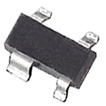
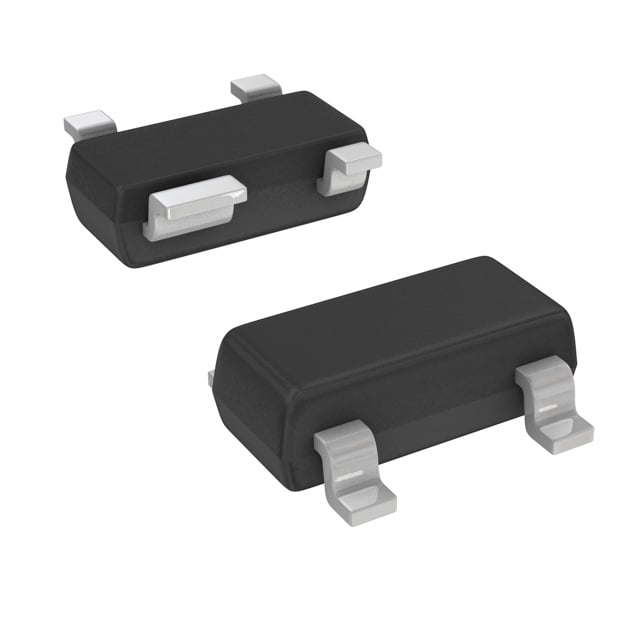
| 描述 | IC SUPERVISOR RESET 3.08V SOT143 |
| 产品分类 | |
| 品牌 | Analog Devices Inc |
| 数据手册 | |
| 产品图片 |
|
| 产品型号 | ADM812TARTZ-REEL7 |
| rohs | 无铅 / 符合限制有害物质指令(RoHS)规范要求 |
| 产品系列 | - |
| 供应商器件封装 | SOT-143-4 |
| 其它名称 | ADM812TARTZ-REEL7-ND |
| 包装 | 带卷 (TR) |
| 受监控电压数 | 1 |
| 复位 | 高有效 |
| 复位超时 | 最小为 140 ms |
| 安装类型 | 表面贴装 |
| 封装/外壳 | TO-253-4,TO-253AA |
| 工作温度 | -40°C ~ 85°C |
| 标准包装 | 3,000 |
| 电压-阈值 | 3.08V |
| 类型 | 简单复位/加电复位 |
| 输出 | 推挽式,图腾柱 |


- 商务部:美国ITC正式对集成电路等产品启动337调查
- 曝三星4nm工艺存在良率问题 高通将骁龙8 Gen1或转产台积电
- 太阳诱电将投资9.5亿元在常州建新厂生产MLCC 预计2023年完工
- 英特尔发布欧洲新工厂建设计划 深化IDM 2.0 战略
- 台积电先进制程称霸业界 有大客户加持明年业绩稳了
- 达到5530亿美元!SIA预计今年全球半导体销售额将创下新高
- 英特尔拟将自动驾驶子公司Mobileye上市 估值或超500亿美元
- 三星加码芯片和SET,合并消费电子和移动部门,撤换高东真等 CEO
- 三星电子宣布重大人事变动 还合并消费电子和移动部门
- 海关总署:前11个月进口集成电路产品价值2.52万亿元 增长14.8%


PDF Datasheet 数据手册内容提取
Microprocessor Supervisory Circuit in 4-Lead SOT-143 with DSP Data Sheet ADM811/ADM812 FEATURES FUNCTIONAL BLOCK DIAGRAM Superior upgrade for MAX811/MAX812 ADM811/ADM812 Specified over temperature Low power consumption: 5 μA typical VCC GENREERSAETTOR RESET/RESET Precision voltage monitor: 2.5 V, 3 V, 3.3 V, 5 V options VREF Reset assertion down to 1 V CC PLoogwiec rl-oown RreEsSeEtT: 1o4u0t pmust m(AiDniMm8u1m1) MR DEBOUNCE GND 00092-001 Figure 1. Logic high RESET output (ADM812) Built-in manual reset APPLICATIONS Microprocessor systems Controllers Intelligent instruments Automotive systems Safety systems Portable instruments GENERAL DESCRIPTION The ADM811/ADM812 are reliable voltage monitoring devices into a state that can only be detected by the user. Allowing the suitable for use in most voltage monitoring applications. The user to reset a system manually can reduce the damage or ADM811/ADM812 are designed to monitor six different voltages, danger that could otherwise be caused by an out-of-control each allowing a 5% or 10% degradation of standard PSU voltages or locked system. before a reset occurs. These voltages have been selected for the effective monitoring of 2.5 V, 3 V, 3.3 V, and 5 V supply voltage levels. VCC VCC ADM811 MICROPROCESSOR Included in this circuit is a debounced manual reset input. SYSTEM Reset can be activated using an electrical switch (or an input MR RESET RESET 100kΩ from another digital device) or by a degradation of the supply GND GND vthoelt caigrec.u Tith ien m wahnicuha lt rhees eAt DfuMnc8t1i1o/nA iDs vMer8y1 2u saerfeu ol,p eesrpaetciniagl leyn itfe rs 00092-002 Figure 2. Typical ADM811 Operating Circuit Rev. H Document Feedback Information furnished by Analog Devices is believed to be accurate and reliable. However, no responsibility is assumed by Analog Devices for its use, nor for any infringements of patents or other One Technology Way, P.O. Box 9106, Norwood, MA 02062-9106, U.S.A. rights of third parties that may result from its use. Specifications subject to change without notice. No license is granted by implication or otherwise under any patent or patent rights of Analog Devices. Tel: 781.329.4700 ©1999–2016 Analog Devices, Inc. All rights reserved. Trademarks and registered trademarks are the property of their respective owners. Technical Support www.analog.com
ADM811/ADM812 Data Sheet TABLE OF CONTENTS Features .............................................................................................. 1 Reset Thresholds ...........................................................................8 Applications ....................................................................................... 1 Reset Output ..................................................................................8 Functional Block Diagram .............................................................. 1 Manual Reset ..................................................................................8 General Description ......................................................................... 1 Glitch Immunity ............................................................................8 Revision History ............................................................................... 2 Interfacing to Other Devices ............................................................9 Specifications ..................................................................................... 3 Output .............................................................................................9 Absolute Maximum Ratings ............................................................ 5 Benefits of a Very Accurate Reset Threshold ............................9 ESD Caution .................................................................................. 5 Ensuring a Valid RESET/Reset Output Down to V = 0 V....9 CC Pin Configuration and Function Descriptions ............................. 6 Outline Dimensions ....................................................................... 10 Typical Performance Characteristics ............................................. 7 Ordering Guide .......................................................................... 10 Circuit Information .......................................................................... 8 REVISION HISTORY 3/16—Rev. G to Rev. H 2/03—Rev. B to Rev. C Changed ADM81x to ADM811/ADM812 ................. Throughout Changes to Features Section ............................................................ 1 Change RESET/RESET Output Voltage Parameter, Table 1 ......... 3 Changes to General Description Section ....................................... 1 Changes to Ordering Guide .......................................................... 10 Changes to Specifications Section ................................................... 2 Removed Note 2 from Ordering Guide .......................................... 3 3/13—Rev. F to Rev. G Changes to Pin Function Descriptions ........................................... 4 Changes to Pin 4 Description; Table 3 ........................................... 5 Removed Note from Table I ............................................................ 6 Updated Outline Dimensions ......................................................... 9 Changes to Ordering Guide .......................................................... 10 1/03—Rev. A to Rev. B Added ADM812 ................................................................. Universal 8/09—Rev. E to Rev. F Changes to Specifications ................................................................. 2 Changes to Ordering Guide .......................................................... 10 Changes to Ordering Guide ............................................................. 3 Changes to Pin Configuration ......................................................... 4 5/08—Rev. D to Rev. E Changes to Pin Function Description ............................................ 4 Changes to Table 2 ............................................................................ 4 Additions to Table I ........................................................................... 6 Updated Outline Dimensions ......................................................... 9 Changes to Manual Reset section .................................................... 6 Changes to Ordering Guide .......................................................... 10 5/02—Rev. 0 to Rev. A 5/06—Rev. C to Rev. D Deleted ADM812 ................................................................ Universal Changes to Ordering Guide ............................................................ 9 4/99—Revision 0: Initial Version Rev. H | Page 2 of 12
Data Sheet ADM811/ADM812 SPECIFICATIONS V = full operating range; T = T to T ; V typical = 5 V for L/M models, 3.3 V for T/S models, 3 V for R model, 2.5 V for Z CC A MIN MAX CC models, unless otherwise noted. Table 1. Parameter Min Typ Max Unit Test Conditions/Comments SUPPLY Voltage 1.0 5.5 V T = 0°C to 70°C A 1.2 V T = −40°C to +85°C A Current 8 15 µA V < 5.5 V, ADM811L/ADM812L/ADM811M/ADM812M, CC I = 0 mA OUT 5 10 µA V < 3.6 V, ADM811R/ADM812R/ADM811S/ADM812S/ CC ADM811T/ADM812T/ADM811Z/ADM812Z, I = 0 mA OUT RESET VOLTAGE THRESHOLD ADM811L/ADM812L 4.54 4.63 4.72 V T = 25°C A ADM811L/ADM812L 4.50 4.75 V T = −40°C to +85°C A ADM811M/ADM812M 4.30 4.38 4.46 V T = 25°C A ADM811M/ADM812M 4.25 4.50 V T = −40°C to +85°C A ADM811T/ADM812T 3.03 3.08 3.14 V T = 25°C A ADM811T/ADM812T 3.00 3.15 V T = −40°C to +85°C A ADM811S/ADM812S 2.88 2.93 2.98 V T = 25°C A ADM811S/ADM812S 2.85 3.00 V T = −40°C to +85°C A ADM811R/ADM812R 2.58 2.63 2.68 V T = 25°C A ADM811R/ADM812R 2.55 2.70 V T = −40°C to +85°C A ADM811Z/ADM812Z 2.28 2.32 2.35 V T = 25°C A ADM811Z/ADM812Z 2.25 2.38 V T = −40°C to +85°C A RESET THRESHOLD TEMPERATURE 30 ppm/°C COEFFICIENT V TO RESET/RESET DELAY 40 µs V = 125 mV, ADM811L/ADM812L/ADM811M/ADM812M CC OD 20 µs V = 125 mV, ADM811R/ADM812R/ADM811S/ADM812S/ OD ADM811T/ADM812T/ADM811Z/ADM812Z RESET ACTIVE TIMEOUT PERIOD 140 560 ms VCC = VTH(MAX) 300 700 ms ADM811-3T only MANUAL RESET Minimum Pulse Width 10 µs Glitch Immunity 100 ns RESET/RESET Propagation Delay 0.5 µs Pull-Up Resistance 10 20 30 kΩ The Manual Reset Circuit Acts On An Input Rising Above 2.3 V V > V , ADM811L/ADM812L/ADM811M/ADM812M CC TH(MAX) An Input Falling Below 0.8 V V > V , ADM811L/ADM812L/ADM811M/ADM812M CC TH(MAX) An Input Rising Above 0.7 × VCC V VCC > VTH(MAX), ADM811R/ADM812R/ADM811S/ADM812S/ ADM811T/ADM812T/ADM811Z/ADM812Z An Input Falling Below 0.25 × V V V > V , ADM811R/ADM812R/ADM811S/ADM812S/ CC CC TH(MAX) ADM811T/ADM812T/ADM811Z/ADM812Z Rev. H | Page 3 of 12
ADM811/ADM812 Data Sheet Parameter Min Typ Max Unit Test Conditions/Comments RESET/RESET Output Voltage Low (ADM812R/ADM812S/ 0.3 V V = V , I = 1.2 mA CC TH(MAX) SINK ADM812T/ADM812Z) Low (ADM812L/ADM812M) 0.4 V V = V , I = 3.2 mA CC TH(MAX) SINK High (ADM812R/ADM812S/ 0.8 × VCC V 1.8 V < VCC < VTH(MIN), ISOURCE = 150 µA ADM812T/ADM812Z/ADM812L/ ADM812M) Low (ADM811R/ADM811S/ 0.3 V V = V I = 1.2 mA CC TH(MIN), SINK ADM811T/ADM811Z) Low (ADM811L/ADM811M) 0.4 V V = V , I = 3.2 mA CC TH(MIN) SINK Low (ADM811R/ADM811S/ 0.3 V V > 1.0 V, I = 50 µA CC SINK ADM811T/ADM811Z/ ADM811L/ADM811M) High (ADM811R/ADM811S/ 0.8 × VCC V VCC > VTH(MAX), ISOURCE = 500 µA ADM811T/ADM811Z) High (ADM811L/ADM811M) V − 1.5 V V > V , I = 800 µA CC CC TH(MAX) SOURCE Rev. H | Page 4 of 12
Data Sheet ADM811/ADM812 ABSOLUTE MAXIMUM RATINGS Typical values are at TA = 25°C, unless otherwise noted. Stresses at or above those listed under Absolute Maximum Ratings may cause permanent damage to the product. This is a Table 2. stress rating only; functional operation of the product at these Parameter Rating or any other conditions above those indicated in the operational Terminal Voltage (With Respect to Ground) section of this specification is not implied. Operation beyond V −0.3 V to +6 V CC the maximum operating conditions for extended periods may All Other Inputs −0.3 V to V + 0.3 V CC affect product reliability. Input Current ESD CAUTION V 20 mA CC MR 20 mA Output Current RESET 20 mA Power Dissipation (T = 70°C) A RA-4 (SOT-143) 200 mW Derate by 4 mW/°C Above 70°C θ Thermal Impedance 330°C/W JA Operating Temperature Range −40°C to +85°C Storage Temperature Range −65°C to +160°C Lead Temperature (Soldering, 10 sec) 300°C Vapor Phase (60 sec) 215°C Infrared (15 sec) 220°C ESD Rating 3 kV Rev. H | Page 5 of 12
ADM811/ADM812 Data Sheet PIN CONFIGURATION AND FUNCTION DESCRIPTIONS GND 1 4 VCC ADM811/ ADM812 RESET/RESET 2 (NToOt Pto V SIEcaWle) 3 MR 00092-003 Figure 3. Pin Configuration Table 3. Pin Function Descriptions Pin No. Mnemonic Description 1 GND Ground Reference For All Signals, 0 V. 2 RESET (ADM811) Active Low Logic Output. RESET remains low while VCC is below the reset threshold or when MR is low; RESET then remains low for at least 140 ms (at least 300 ms for the ADM811-3T) after V rises above the CC reset threshold. RESET (ADM812) Active High Logic Output. RESET remains high while V is below the reset threshold or when MR is low; CC RESET then remains high for 240 ms (typical) after V rises above the reset threshold. CC 3 MR Manual Reset. This active low debounced input ignores input pulses of 100 ns or less (typical) and is guaranteed to accept input pulses of greater than 10 μs. Leave floating when not used. 4 VCC Monitored Supply Voltage of 2.5 V, 3 V, 3.3 V, or 5 V. A 0.1 μF decoupling capacitor between VCC and the GND pin is recommended. Rev. H | Page 6 of 12
Data Sheet ADM811/ADM812 TYPICAL PERFORMANCE CHARACTERISTICS 12 10 IDD @ VCC = 5.5V 9 10 IDD @ VCC = 5.5V 8 7 8 A) IDD @ VCC = 3V A) 6 IDD @ VCC = 3V µ µ (D 6 (D 5 D D I I 4 4 3 2 2 IDD @ VCC = 1V 1 IDD @ VCC = 1V 0 0 –40 –20 0 20TEM3P0ERAT5U0RE (°7C0) 85 100 120 00092-004 –40 –20 0 20TEM3P0ERAT5U0RE (°7C0) 85 100 120 00092-007 Figure 4. Supply Current vs. Temperature Figure 7. Supply Current vs. Temperature (ADM811L/ADM812L/ (ADM811R/ADM812R/ADM811S/ADM812S/ ADM811M/ADM812M) ADM811T/ADM812T/ADM811Z/ADM812Z) 1000 900 900 800 Y (µs) 800 Y (µs) 700 A A L 700 L E E 600 D D T 600 T SE SE 500 RE 500 RE N N 400 R-DOW 430000 VOD = 20mV R-DOW 300 VOD = 20mV E E W W 200 PO 210000 VOD = 125mVVOD = 200mV PO 100 VOD = 125mV 0 0 VOD = 200mV –40 –20 0 20TEM3P0ERAT5U0RE (7°C0) 85 100 120 00092-005 –40 –20 0 20TEM3P0ERAT5U0RE (°7C0) 85 100 120 00092-008 Figure 5. Power-Down RESET Delay vs. Temperature Figure 8. Power-Down RESET Delay vs. Temperature (ADM811L/ADM812L/ (ADM811R/ADM812R/ADM811S/ADM812S/ ADM811M/ADM812M) ADM811T/ADM812T/ADM811Z/ADM812Z) 299 1.007 1.006 294 s) ADM81xL/M LD1.005 T (m 279 SHO1.004 U E1.003 O 274 R ME TH1.002 RESET TI 226694 D RESET 11..000012 R-UP 259 ALIZE01..909090 E M OW 254 OR0.998 P ADM81xR/S/T/Z N0.997 249 0.996 244–40 –20 0 20TEM3P0ERAT5U0RE (°7C0) 85 100 120 00092-006 0.995–40 –20 0 20TEM3P0ERAT5U0RE (°7C0) 85 100 120 00092-009 Figure 6. Power-Up RESET Timeout vs. Temperature Figure 9. RESET Threshold Deviation vs. Temperature Rev. H | Page 7 of 12
ADM811/ADM812 Data Sheet CIRCUIT INFORMATION RESET THRESHOLDS The ADM811 provides an active low reset output (RESET) while the ADM812 provides an active high output (RESET). A reset output is provided to the microprocessor whenever the V input is below the reset threshold. The actual reset threshold During power-down of the ADM811, the RESET output CC depends on whether an L, M, T, S, R, or Z suffix is used (see remains valid (low) with VCC as low as 1 V. This ensures that the Table 4). microprocessor is held in a stable shutdown condition as the supply falls and also ensures that no spurious activity can Table 4. Reset Threshold Options occur via the microprocessor as it powers up. Model Reset Threshold (V) MANUAL RESET ADM811LART 4.63 ADM811MART 4.38 The ADM811/ADM812 are equipped with a manual reset ADM811TART 3.08 input. This input is designed to operate in a noisy environment ADM811-3TART 3.08 where unwanted glitches could be induced. These glitches could ADM811SART 2.93 be produced by the bouncing action of a switch contact, or where a ADM811RART 2.63 manual reset switch may be located some distance away from ADM811ZART 2.32 the circuit (the cabling of which can pick up noise). ADM812LART 4.63 The manual reset input is guaranteed to ignore logically valid ADM812MART 4.38 inputs that are faster than 100 ns and to accept inputs longer in ADM812TART 3.08 duration than 10 µs. ADM812SART 2.93 GLITCH IMMUNITY ADM812RART 2.63 ADM812ZART 2.32 The ADM811/ADM812 contain internal filtering circuitry providing glitch immunity from fast transient glitches on the RESET OUTPUT power supply line. On power-up and after V rises above the reset threshold, an CC VCC VREF VREF VREF VREF internal timer holds the reset output active for 240 ms (typical). This is intended as a power-on reset signal for the processor. It RESET t1 t1 allows time for both the power supply and the microprocessor itnot setrarbuiplitzieo na fotecrc uprosw, tehr-eu rpe.s Ieft ao uptopwuetr i ss usipmpliyla brlryo wacntiovuatt eodr and tV1R =E FR =E SREETS ETTIM VEO =L T25A0GmEs TTHYRPEICSAHLOLD 00092-010 remains active for 240 ms (typical) after the supply recovers. Figure 10. Power Fall RESET Timing This allows time for the power supply and microprocessor to stabilize. Rev. H | Page 8 of 12
Data Sheet ADM811/ADM812 INTERFACING TO OTHER DEVICES OUTPUT VCC The ADM811/ADM812 are designed to integrate with as many VCC devices as possible. One feature of the ADM811/ADM812 is the ADM811 reset output, which is directly proportional to V (this is guar- CC RESET anteed only while V is greater than 1 V). This enables the part CC GND ttoh eb me uinseimd uwmit ha nbdo tmh a3x Vim aunmd 5sp Ve,c oifri caantyio nnosm foirn aVl CvCo. ltage within 00092-011 BENEFITS OF A VERY ACCURATE RESET Figure 11. Ensuring a Valid RESET Output Down to VCC = 0 V THRESHOLD ENSURING A VALID RESET/RESET OUTPUT DOWN Because the ADM811/ADM812 can operate effectively even TO VCC = 0 V when there are large degradations of the supply voltages, the When V falls below 0.8 V, the RESET/RESET of the ADM811/ CC possibility of a malfunction during a power failure is greatly ADM812 no longer sinks current. Therefore, a high impedance reduced. Another advantage of the ADM811/ADM812 are the CMOS logic input connected to RESET/RESET can drift to very accurate internal voltage reference circuits. Combined, undetermined logic levels. To eliminate this problem, a 100 kΩ these benefits produce an exceptionally reliable microprocessor resistor should be connected from RESET/RESET to ground. supervisory circuit. Rev. H | Page 9 of 12
ADM811/ADM812 Data Sheet OUTLINE DIMENSIONS 3.04 2.90 2.80 1.92 BSC 0.20 BSC 4 3 2.64 1.40 2.10 1.30 1.20 1 2 1.72 REF 1.07 1.22 0.90 0.80 0.75 0.100 0.20 8° 0.013 0.08 0° 0.60 0.89 0.50 SEATING 0.50 0.76 0.30 PLANE 0.54 REF 0.40 COMPLIANTTO JEDEC STANDARDSTO-253-AA 03-13-2012-B Figure 12. 4-Lead Small Outline Transistor Package [SOT-143] (RA-4) Dimensions shown in millimeters ORDERING GUIDE Reset Temperature Ordering Package Model1, 2 Threshold (V) Range Quantity Description Package Option Branding ADM811LART-REEL7 4.63 –40°C to +85°C 3,000 4-Lead SOT-143 RA-4 MBV ADM811LARTZ-REEL7 4.63 –40°C to +85°C 3,000 4-Lead SOT-143 RA-4 M4J ADM811MARTZ-REEL 4.38 –40°C to +85°C 10,000 4-Lead SOT-143 RA-4 MBT # ADM811MARTZ-REEL7 4.38 –40°C to +85°C 3,000 4-Lead SOT-143 RA-4 MBT # ADM811TART-REEL7 3.08 –40°C to +85°C 3,000 4-Lead SOT-143 RA-4 MBG ADM811TARTZ-REEL 3.08 –40°C to +85°C 10,000 4-Lead SOT-143 RA-4 MBG # ADM811TARTZ-REEL7 3.08 –40°C to +85°C 3,000 4-Lead SOT-143 RA-4 MBG # ADM811-3TART-REEL7 3.08 –40°C to +85°C 3,000 4-Lead SOT-143 RA-4 MB3 ADM811-3TARTZ-RL7 3.08 –40°C to +85°C 3,000 4-Lead SOT-143 RA-4 M4E ADM811SART-REEL7 2.93 –40°C to +85°C 3,000 4-Lead SOT-143 RA-4 MBE ADM811SARTZ-REEL 2.93 –40°C to +85°C 10,000 4-Lead SOT-143 RA-4 MBE # ADM811SARTZ-REEL7 2.93 –40°C to +85°C 3,000 4-Lead SOT-143 RA-4 MBE # ADM811RARTZ-REEL7 2.63 –40°C to +85°C 3,000 4-Lead SOT-143 RA-4 M4N ADM811ZART-REEL7 2.32 –40°C to +85°C 3,000 4-Lead SOT-143 RA-4 MBZ ADM811ZARTZ-REEL7 2.32 –40°C to +85°C 3,000 4-Lead SOT-143 RA-4 M6G ADM812LARTZ-REEL7 4.63 –40°C to +85°C 3,000 4-Lead SOT-143 RA-4 M5D ADM812MARTZ-REEL7 4.38 –40°C to +85°C 3,000 4-Lead SOT-143 RA-4 M6D ADM812TARTZ-REEL7 3.08 –40°C to +85°C 3,000 4-Lead SOT-143 RA-4 M68 ADM812SARTZ-REEL 2.93 –40°C to +85°C 10,000 4-Lead SOT-143 RA-4 M67 ADM812SARTZ-REEL7 2.93 –40°C to +85°C 3,000 4-Lead SOT-143 RA-4 M67 ADM812RARTZ-REEL7 2.63 –40°C to +85°C 3,000 4-Lead SOT-143 RA-4 M6F ADM812ZARTZ-REEL7 2.32 –40°C to +85°C 3,000 4-Lead SOT-143 RA-4 M69 1 Available only in reels. 2 Z = RoHS Compliant Part. RoHS-compliant parts may have # branded on either the top or bottom of the device. Rev. H | Page 10 of 12
Data Sheet ADM811/ADM812 NOTES Rev. H | Page 11 of 12
ADM811/ADM812 Data Sheet NOTES ©1999–2016 Analog Devices, Inc. All rights reserved. Trademarks and registered trademarks are the property of their respective owners. D00092-0-3/16(H) Rev. H | Page 12 of 12