ICGOO在线商城 > 集成电路(IC) > 接口 - 驱动器,接收器,收发器 > ADM202JRNZ

 Datasheet下载
- 型号: ADM202JRNZ
- 制造商: Analog
- 库位|库存: xxxx|xxxx
- 要求:
| 数量阶梯 | 香港交货 | 国内含税 |
| +xxxx | $xxxx | ¥xxxx |
查看当月历史价格
查看今年历史价格
ADM202JRNZ产品简介:
ICGOO电子元器件商城为您提供ADM202JRNZ由Analog设计生产,在icgoo商城现货销售,并且可以通过原厂、代理商等渠道进行代购。 ADM202JRNZ价格参考¥-¥13.18。AnalogADM202JRNZ封装/规格:接口 - 驱动器,接收器,收发器, 全 收发器 2/2 RS232 16-SOIC。您可以下载ADM202JRNZ参考资料、Datasheet数据手册功能说明书,资料中有ADM202JRNZ 详细功能的应用电路图电压和使用方法及教程。
| 参数 | 数值 |
| 产品目录 | 集成电路 (IC)半导体 |
| 描述 | IC TX/RX RS-232 5V 15KV 16SOICRS-232接口集成电路 2 CH 15KV ESD Protected IC |
| 产品分类 | |
| 品牌 | Analog Devices Inc |
| 产品手册 | |
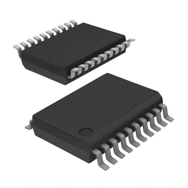
| 产品图片 |
|
| rohs | 符合RoHS无铅 / 符合限制有害物质指令(RoHS)规范要求 |
| 产品系列 | 接口 IC,RS-232接口集成电路,Analog Devices ADM202JRNZ- |
| 数据手册 | |
| 产品型号 | ADM202JRNZ |
| 产品目录页面 | |
| 产品种类 | RS-232接口集成电路 |
| 供应商器件封装 | 16-SOIC N |
| 关闭 | No |
| 功能 | Transceiver |
| 包装 | 管件 |
| 协议 | RS232 |
| 双工 | 全 |
| 商标 | Analog Devices |
| 安装类型 | 表面贴装 |
| 安装风格 | SMD/SMT |
| 封装 | Tube |
| 封装/外壳 | 16-SOIC(0.154",3.90mm 宽) |
| 封装/箱体 | SOIC-16 |
| 工作温度 | 0°C ~ 70°C |
| 工作温度范围 | 0 C to + 70 C |
| 工作电源电压 | 4.5 V to 5.5 V |
| 工厂包装数量 | 48 |
| 接收器滞后 | 400mV |
| 接收机数量 | 2 Receiver |
| 支持协议 | RS-232 |
| 数据速率 | - |
| 最大工作温度 | + 70 C |
| 最小工作温度 | 0 C |
| 标准包装 | 48 |
| 激励器数量 | 2 Driver |
| 电压-电源 | 4.5 V ~ 5.5 V |
| 电源电流 | 6 mA |
| 类型 | 收发器 |
| 系列 | ADM202 |
| 驱动器/接收器数 | 2/2 |


PDF Datasheet 数据手册内容提取
High Speed, 5 V, 0.1 µF CMOS RS-232 Driver/Receiver Data Sheet ADM202 FEATURES TYPICAL APPLICATION CIRCUIT 120 kB transmission rate 5V INPUT Small (0.1 µF) charge pump capacitors Single 5 V power supply 0.1µF + 1 C1+ +5VVO TLOTA +G1E0V VCC 16 0.1µF +06..13µVF Meets TIA/EIA-232-E and V.28 specifications 6.3V DOUBLER +6.3V 3 C1– V+ 2 2 drivers and 2 receivers O±9n -Vb oouatrpdu dtc s-wtoi-ndgc wcoitnhv 5e rVte srusp ply 0.116µVF + 45 CC22–+ +1IVN0OVV LETTROAT G–E1ER0V V– 6 +01.61VµF Low power BiCMOS: 2.5 mA I CC ±30 V receiver input levels T1IN 11 T1 14 T1OUT TTL/CMOS RS-232 INPUTS1 OUTPUTS APPLICATIONS T2IN 10 T2 7 T2OUT Computers R1OUT 12 R1 13 R1IN TTL/CMOS RS-232 Peripherals OUTPUTS INPUTS2 Modems R2OUT 9 R2 8 R2IN Printers GND ADM202 15 Instruments 12IINNTTEERRNNAALL 54k0Ω0k PΩU PLULL-DLO-UWPN R RESEISSITSOTORR O ONN E AEACCHH T TRLS/-C2M32O ISN PINUPTU.T. 00065-001 Figure 1. GENERAL DESCRIPTION The ADM202 is a 2-channel RS-232 line driver/receiver pair An epitaxial BiCMOS construction minimizes power consump- designed to operate from a single 5 V power supply. A highly tion to 10 mW and guards against latch-up. Overvoltage efficient on-chip charge pump design permits RS-232 levels to protection is provided, allowing the receiver inputs to withstand be developed using charge pump capacitors as small as 0.1 µF. continuous voltages in excess of ±30 V. In addition, all pins This converter generates ±10 V RS-232 output levels. contain ESD protection to levels greater than 2 kV. The ADM202 meets or exceeds the TIA/EIA-232-E and V.28 The ADM202 is available in a 16-lead PDIP and both narrow specifications. Fast driver slew rates permit 120 kB operation, and wide 16-lead SOIC packages. and high drive currents allow extended cable lengths. Rev. B Document Feedback Information furnished by Analog Devices is believed to be accurate and reliable. However, no responsibility is assumed by Analog Devices for its use, nor for any infringements of patents or other One Technology Way, P.O. Box 9106, Norwood, MA 02062-9106, U.S.A. rights of third parties that may result from its use. Specifications subject to change without notice. No license is granted by implication or otherwise under any patent or patent rights of Analog Devices. Tel: 781.329.4700 ©2016 Analog Devices, Inc. All rights reserved. Trademarks and registered trademarks are the property of their respective owners. Technical Support www.analog.com
ADM202 Data Sheet TABLE OF CONTENTS Features .............................................................................................. 1 Typical Performance Characteristics ..............................................6 Applications ....................................................................................... 1 Theory of Operation .........................................................................7 Typical Application Circuit ............................................................. 1 Applications Information .................................................................8 General Description ......................................................................... 1 Charge Pump DC-to-DC Voltage Converter ............................8 Revision History ............................................................................... 2 TTL/CMOS to RS-232 Transmitters (Drivers) .........................8 Specifications ..................................................................................... 3 RS-232 to TTL/CMOS Receivers ................................................8 Absolute Maximum Ratings ............................................................ 4 Outline Dimensions ..........................................................................9 ESD Caution .................................................................................. 4 Ordering Guide .......................................................................... 10 Pin Configuration and Function Descriptions ............................. 5 REVISION HISTORY 8/2016—Rev. A to Rev. B Changes to Table 2 ............................................................................. 4 Updated Format .................................................................. Universal Changes to Table 3 ............................................................................. 5 Deleted ADM203 ................................................................ Universal Changes to Theory of Operation Section....................................... 7 Changes to Typical Application Circuit Section Heading........... 1 Changes to TTL/CMOS to RS-232 Transmitters (Drivers) Deleted ADM203 Functional Block Diagram Figure; Section and RS-232 to TLL/CMOS Receivers Section ................. 8 Renumbered Sequentially ................................................................ 1 Updated Outline Dimensions .......................................................... 9 Changes to Features Section and General Description Section . 1 Changes to Ordering Guide .......................................................... 10 Deleted ADM203 Pin Configuration Figure and Figure 1 ......... 3 Changed T to Tx ....................................................... Throughout 1/2001—Rev. 0 to Rev. A IN IN Rev. B | Page 2 of 10
Data Sheet ADM202 SPECIFICATIONS V = 5 V ± 10%, (C1 to C4 = 0.1 µF). All specifications T to T , unless otherwise noted. CC MIN MAX Table 1. Parameter Min Typ Max Unit Test Conditions/Comments OUTPUT VOLTAGE SWING ±5 ±9 V V = 5 V ± 5%; T1 and T2 loaded with 3 kΩ to GND CC OUT OUT ±5 ±9 V V = 5 V ± 10%; T = 25°C; T1 and T2 loaded with 3 kΩ to GND CC A OUT OUT V POWER SUPPLY CURRENT (I ) 2.5 6.0 mA No load; T1 and T2 = V , or T1 and T2 = GND CC CC IN IN CC IN IN INPUT LOGIC THRESHOLD Low, V 0.8 V Tx INL IN High, V 2.4 V Tx INH IN LOGIC PULL-UP CURRENT 12 25 µA Tx = 0 V IN RS-232 INPUT Voltage Range −30 +30 V Threshold Low 0.8 1.2 V High 1.6 2.4 V Hysteresis 0.2 0.4 1.0 V Resistance 3 5 7 kΩ T = 0°C to 85°C A TTL/CMOS Output Voltage Low, V 0.4 V I = 1.6 mA OL OUT High, V 3.5 V I = –1.0 mA OH OUT PROPAGATION DELAY 0.3 5 µs RS-232 to TTL TRANSITION REGION SLEW RATE 8 V/µs R = 3 kΩ, C = 1000 pF, measured from +3 V to –3 V or –3 V to +3 V L L BAUD RATE 120 kB R = 3 kΩ, C = 1 nF L L OUTPUT Output Resistance 300 Ω V = V+ = V– = 0 V, V = ±2 V CC OUT RS-232 Output Short-Circuit Current ±10 ±60 mA Rev. B | Page 3 of 10
ADM202 Data Sheet ABSOLUTE MAXIMUM RATINGS T = 25°C, unless otherwise noted. Stresses at or above those listed under Absolute Maximum A Ratings may cause permanent damage to the product. This is a Table 2. stress rating only; functional operation of the product at these Parameter Rating or any other conditions above those indicated in the operational V 6 V CC section of this specification is not implied. Operation beyond V+ (V − 0.3 V) to +14 V CC the maximum operating conditions for extended periods may V– +0.3 V to −14 V affect product reliability. Input Voltages T1 , T2 −0.3 V to (V + 0.3 V) IN IN CC R1 , R2 ±30 V ESD CAUTION IN IN Output Voltages T1 , T2 ((V+) + 0.3 V) to ((V−) − 0.3 V) OUT OUT R1 , R2 –0.3 V to (V + 0.3 V) OUT OUT CC Short-Circuit Duration T1 , T2 Continuous OUT OUT Power Dissipation 16-Lead PDIP (N-16) 470 mW 16-Lead SOIC (R-16) 600 mW 16-Lead SOIC (RW-16) 500 mW Thermal Impedance, θ JA 16-Lead PDIP (N-16) 135°C/W 16-Lead SOIC (R-16) 105°C/W 16-Lead SOIC (RW-16) 105°C/W Operating Temperature Range Commercial (J Version) 0°C to 70°C Storage Temperature Range −65°C to +150°C Lead Temperature Soldering Vapor Phase (60 sec) 215°C Infrared (15 sec) 220°C ESD Rating >2000 V Rev. B | Page 4 of 10
Data Sheet ADM202 PIN CONFIGURATION AND FUNCTION DESCRIPTIONS C1+ 1 16 VCC V+ 2 15 GND C1– 3 ADM202 14 T1OUT C2+ 4 TOP VIEW 13 R1IN C2– 5 (Not to Scale) 12 R1OUT V– 6 11 T1IN T2RO2UINT 78 190 RT22IONUT 00065-002 Figure 2. Pin Configuration Table 3. Pin Function Descriptions Pin No. Mnemonic Description 1 C1+ External Positive Capacitor 1 Connection. The positive terminal is connected to this pin. 2 V+ Internally Generated Positive Supply (+10 V nominal). 3 C1− External Negative Capacitor 1 Connection. The negative terminal is connected to this pin. 4 C2+ External Positive Capacitor 2 Connection. The positive terminal is connected to this pin. 5 C2− External Negative Capacitor 1 Connection. The negative terminal is connected to this pin. 6 V− Internally Generated Negative Supply (−10 V Nominal). 7, 14 T2 , T1 Transmitter (Driver) Outputs. These outputs are RS-232 levels (typically ±10 V). OUT OUT 8, 13 R2 , R1 Receiver Inputs. These inputs accept RS-232 signal levels. An internal 5 kΩ pull-down resistor to GND is IN IN connected on each of these inputs. 9, 12 R2 , R1 Receiver Outputs. These outputs are TTL/CMOS levels. OUT OUT 10, 11 T2 , T1 Transmitter (Driver) Inputs. These inputs accept TTL/CMOS levels. An internal 400 kΩ pull-up resistor to V is IN IN CC connected on each input. 15 GND Ground. This pin must be connected to 0 V. 16 V Power Supply Input, 5 V ± 10%. CC Rev. B | Page 5 of 10
ADM202 Data Sheet TYPICAL PERFORMANCE CHARACTERISTICS 15 15 Tx OUTPUT HIGH 10 10 V+ V) 5 GE( 5 Tx OUTPUT HIGH LOADED A V– (V) 0 VOLT 0 V+, PUT T –5 OU –5 Tx OUTPUT LOW LOADED x V– T –10 –10 Tx OUTPUT LOW –150 5 1L0OAD CUR15RENT (mA2)0 25 30 00065-003 –154.0 4.5 VCC (V) 5.0 5.5 00065-006 Figure 3. Charge Pump V+, V− vs. Load Current Figure 6. Transmitter (Tx) Output Voltage vs. VCC 30 15 VCC = 5V RL = 3kΩ 25 f = 10kHz 10 Tx OUTPUT HIGH V) µs) 20 GE ( 5 V/ A E ( LT AT 15 VO 0 W R LOW-TO-HIGH SLEW RATE UT SLE 10 OUTP –5 x T HIGH-TO-LOW SLEW RATE Tx OUTPUT LOW 5 –10 00 0.5k 1C.0AkPACITI1V.E5k LOAD (2p.F0k) 2.5k 3.0k 00065-004 –150 2 4 LOAD6 CURREN8T (mA) 10 12 14 00065-007 Figure 4. Transmitter Slew Rate vs. Capacitive Load Figure 7. Transmitter (Tx) Output Voltage vs. Load Current T T 1 1 2 2 CCHH11 1100..00VV CH2 L 5O.0A0DVED SLEMW1 .R0A0µTsE (1nF) CH1 –6.4V 00065-005 CCHH11 1100..00VV CH2 5U.0N0LVOADED MS1L.E00Wµ sRATE CH2 –6.4V 00065-008 Figure 5. Transmitter Fully Loaded Slew Rate Figure 8. Transmitter Unloaded Slew Rate Rev. B | Page 6 of 10
Data Sheet ADM202 THEORY OF OPERATION The ADM202 is an RS-232 driver/receiver designed to solve on the same chip. CMOS technology keeps the power dissipation interface problems by meeting the TIA/EIA-232E specifications to an absolute minimum. while using a single digital 5 V supply. The EIA standard The ADM202 contains an internal voltage doubler and a voltage requires that transmitters deliver ±5 V minimum on the inverter that generates ±10 V from the 5 V input. External transmission channel and that receivers can accept signal levels 0.1 μF capacitors are required for the internal voltage converter. down to ±3 V. The device achieves this by integrating step-up voltage converters and level shifting transmitters and receivers Rev. B | Page 7 of 10
ADM202 Data Sheet APPLICATIONS INFORMATION The internal circuitry consists of three main sections, as follows: TTL/CMOS TO RS-232 TRANSMITTERS (DRIVERS) • A charge pump dc-to-dc voltage converter The drivers convert TTL/CMOS input levels into TIA/EIA-232-E • TTL/CMOS to RS-232 transmitters output levels. With V = 5 V and driving a typical TIA/EIA-232-E CC • RS-232 to TTL/CMOS receivers load, the output voltage swing is ±9 V. Even under worst case conditions, the drivers are guaranteed to meet the ±5 V TIA/EIA- CHARGE PUMP DC-TO-DC VOLTAGE CONVERTER 232-E minimum requirement. The charge pump voltage converter consists of an oscillator and The input threshold levels are both TTL and CMOS compatible a switching matrix. The converter generates a ±10 V supply from with the switching threshold set at V /4. With a nominal V = CC CC the input 5 V level in two stages, using a switched capacitor 5 V, the switching threshold is 1.25 V typical. Unused inputs can technique as illustrated in Figure 9 and Figure 10. First, the 5 V be left unconnected, as an internal 400 kΩ pull-up resistor pulls input supply is doubled to 10 V using Capacitor C1 as the them high, forcing the outputs into a low state. charge storage element. The 10 V level is then inverted to As required by the TIA/EIA-232-E standard, the slew rate is generate −10 V using C2 as the storage element. limited to less than 30 V/µs without the need for an external Capacitors C3 and C4 reduce the output ripple. Their values are slew limiting capacitor, and the output impedance in the power- not critical and can be reduced if higher levels of ripple are down state is greater than 300 Ω. acceptable. The charge pump capacitors, C1 and C2, can also be RS-232 TO TTL/CMOS RECEIVERS reduced at the expense of higher output impedance on the V+ and V− supplies. The receivers are inverting level shifters that accept TIA/EIA-232-E input levels (±5 V to ±15 V) and translate them into 5 V TTL/ The V+ and V− supplies can be used to power external circuitry CMOS levels. The inputs have internal 5 kΩ pull-down resistors if the current requirements are small. to ground and are protected against overvoltages of up to ±30 V. S1 S3 VCC V+ = 2VCC The guaranteed switching thresholds are 0.8 V (VINL) and 2.4 V C1 + C3 + (VINH), which are well within the ±3 V TIA/EIA-232-E require- S2 S4 ment. The low level threshold is deliberately positive because it GND VCC ensures that an unconnected input is interpreted as a low level. OISNCTIELRLANTAOLR 00065-009 Tlehvee lr oefc e0i.v5e Vrs. Thahvise hay Ssctehrmesiitst ltervigegl eernesdu irnesp uert rworit hfr eae h ryescteepretisoisn , Figure 9. Charge Pump Voltage Doubler both for noisy inputs and for inputs with slow transition times. S1 S3 V+ GND FROM VOLTAGE C2 + C4 + DOUBLER S2 S4 GND V– = –(V+) OISNCTIELRLANTAOLR 00065-010 Figure 10. Charge Pump Voltage Inverter Rev. B | Page 8 of 10
Data Sheet ADM202 OUTLINE DIMENSIONS 0.775 0.755 0.735 16 9 0.280 PIN 1 0.250 INDICATOR 1 0.240 8 TOP VIEW 0.100 0.325 BSC 0.195 0.310 0.210 0.130 0.300 MAX SIDE VIEW 0.115 0.015 0.150 MIN 0.015 0.130 GAUGE END VIEW PLANE 0.012 0.115 SEATING 0.010 PLANE 0.022 0.021 0.430 0.008 0.018 0.070 0.016 MAX 0.015 0.045 0.060 0.011 0.039 0.055 0.030COMPLIANTTO JEDEC STANDARDS MS-001-BB 03-07-2014-D Figure 11. 16-Lead Plastic Dual In-Line Package [PDIP] Narrow Body (N-16) Dimensions shown in inches 10.00 (0.3937) 9.80 (0.3858) 16 9 4.00 (0.1575) 6.20 (0.2441) 3.80 (0.1496) 1 8 5.80 (0.2283) 1.27 (0.0500) 0.50 (0.0197) BSC 45° 1.75 (0.0689) 0.25 (0.0098) 0.25 (0.0098) 1.35 (0.0531) 8° 0.10 (0.0039) 0° COPLANARITY SEATING 0.10 0.51 (0.0201) PLANE 0.25 (0.0098) 1.27 (0.0500) 0.31 (0.0122) 0.17 (0.0067) 0.40 (0.0157) COMPLIANTTO JEDEC STANDARDS MS-012-AC C(RINEOFNPEATRRREOENNLCLTEIHN EOGSN EDLSIYM)AEANNRDSEI AORRNOESU NANORDEET DAIN-PO MPFRIFLO LMPIIMRLELIATIMTEEER TFSEO; RIRN ECUQHSU EDI VIINMA LEDENENSSTIIOGSN NFS.OR 060606-A Figure 12. 16-Lead Standard Small Outline Package [SOIC_N] Narrow Body (R-16) Dimensions shown in millimeters and (inches) Rev. B | Page 9 of 10
ADM202 Data Sheet 10.50(0.4134) 10.10(0.3976) 16 9 7.60(0.2992) 7.40(0.2913) 1 8 10.65(0.4193) 10.00(0.3937) 1.27(0.0500) 0.75(0.0295) BSC 2.65(0.1043) 0.25(0.0098) 45° 0.30(0.0118) 2.35(0.0925) 8° 0.10(0.0039) 0° COPLANARITY 0.10 0.51(0.0201) SPELAATNIENG 0.33(0.0130) 1.27(0.0500) 0.31(0.0122) 0.20(0.0079) 0.40(0.0157) (RCINOEFNPEATRRREOENNLCLTEIHNCEOGOSNDMELISPYM)LAEAIANNRNDSETIAORTRNOOESUJNANEORDDETEEDAICN-POSMPFTRIFALONLMPIDMIRLAELIRATIMTDEEESRTFSMEO;SRIRN-0ECU1QH3SU-EADIVAIINMAELDENENSSTIIOGSNNFS.OR 03-27-2007-B Figure 13. 16-Lead Standard Small Outline Package [SOIC_W] Wide Body (RW-16) Dimensions shown in millimeters and (inches) ORDERING GUIDE Model1 Temperature Range Package Description Package Option ADM202JNZ 0°C to 70°C 16-Lead Plastic Dual In-Line Package [PDIP] N-16 ADM202JRN 0°C to 70°C 16-Lead Standard Small Outline Package [SOIC_N] R-16 ADM202JRN-REEL 0°C to 70°C 16-Lead Standard Small Outline Package [SOIC_N] R-16 ADM202JRN-REEL7 0°C to 70°C 16-Lead Standard Small Outline Package [SOIC_N] R-16 ADM202JRNZ 0°C to 70°C 16-Lead Standard Small Outline Package [SOIC_N] R-16 ADM202JRNZ-REEL 0°C to 70°C 16-Lead Standard Small Outline Package [SOIC_N] R-16 ADM202JRNZ-REEL7 0°C to 70°C 16-Lead Standard Small Outline Package [SOIC_N] R-16 ADM202JRWZ 0°C to 70°C 16-Lead Standard Small Outline Package [SOIC_W] RW-16 ADM202JRWZ-REEL 0°C to 70°C 16-Lead Standard Small Outline Package [SOIC_W] RW-16 1 Z = RoHS Compliant Part. ©2016 Analog Devices, Inc. All rights reserved. Trademarks and registered trademarks are the property of their respective owners. D00065-0-8/16(B) Rev. B | Page 10 of 10
Mouser Electronics Authorized Distributor Click to View Pricing, Inventory, Delivery & Lifecycle Information: A nalog Devices Inc.: ADM202JRW ADM202JRN-REEL7 ADM202JRNZ-REEL ADM202JRN ADM202JN ADM202JRWZ-REEL ADM202JRNZ-REEL7 ADM202JRWZ ADM202JNZ ADM202JRNZ ADM202JRW-REEL