ICGOO在线商城 > 集成电路(IC) > PMIC - 热插拔控制器 > ADM1275-1ACPZ
 Datasheet下载
- 型号: ADM1275-1ACPZ
- 制造商: Analog
- 库位|库存: xxxx|xxxx
- 要求:
| 数量阶梯 | 香港交货 | 国内含税 |
| +xxxx | $xxxx | ¥xxxx |
查看当月历史价格
查看今年历史价格
ADM1275-1ACPZ产品简介:
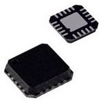
ICGOO电子元器件商城为您提供ADM1275-1ACPZ由Analog设计生产,在icgoo商城现货销售,并且可以通过原厂、代理商等渠道进行代购。 ADM1275-1ACPZ价格参考。AnalogADM1275-1ACPZ封装/规格:PMIC - 热插拔控制器, Hot Swap Controller, Monitor 1 Channel General Purpose 20-LFCSP-WQ (5x5)。您可以下载ADM1275-1ACPZ参考资料、Datasheet数据手册功能说明书,资料中有ADM1275-1ACPZ 详细功能的应用电路图电压和使用方法及教程。
| 参数 | 数值 |
| 产品目录 | 集成电路 (IC)半导体 |
| 描述 | IC HOT SWAP CTRL PMBUS 20LFCSP热交换电压控制器 Low volt Positive Hot Swap + Power mon |
| DevelopmentKit | EVAL-ADM1275EBZ |
| 产品分类 | |
| 品牌 | Analog Devices Inc |
| 产品手册 | |
| 产品图片 |
|
| rohs | 符合RoHS无铅 / 符合限制有害物质指令(RoHS)规范要求 |
| 产品系列 | 电源管理 IC,热交换电压控制器,Analog Devices ADM1275-1ACPZ- |
| 数据手册 | |
| 产品型号 | ADM1275-1ACPZ |
| PCN组件/产地 | |
| PCN设计/规格 | |
| 产品 | Controllers & Switches |
| 产品种类 | 热交换电压控制器 |
| 供应商器件封装 | 20-LFCSP-WQ(5x5) |
| 内部开关 | 无 |
| 功能引脚 | FLB, ISET, (GPO1, /ALERT, CONV), (GPO2, /ALERT2), /LATCH, OV, PWRGD, SS, TIMER, UV, VCAP |
| 包装 | 托盘 |
| 可编程特性 | 自动重试,限流,故障超时,闭锁故障,OVP,UVLO |
| 商标 | Analog Devices |
| 安装类型 | 表面贴装 |
| 安装风格 | SMD/SMT |
| 封装 | Tray |
| 封装/外壳 | 20-WQFN 裸露焊盘,CSP |
| 封装/箱体 | LFCSP-20 |
| 工作温度 | -40°C ~ 85°C |
| 工作温度范围 | - 40 C to + 85 C |
| 工厂包装数量 | 490 |
| 应用 | 通用 |
| 标准包装 | 1 |
| 特性 | PMBus |
| 电压-电源 | 2.95 V ~ 20 V |
| 电流-电源 | 5mA |
| 电流-输出(最大值) | - |
| 电流限制 | Adj |
| 电源电压-最大 | 20 V |
| 电源电压-最小 | 2.95 V |
| 电源电流 | 5 mA |
| 类型 | 热交换控制器, 监控器 |
| 系列 | ADM1275 |
| 输入/电源电压—最大值 | 20 V |
| 输入/电源电压—最小值 | 2.95 V |
| 通道数 | 1 |
| 配用 | /product-detail/zh/EVAL-ADM1275EBZ/EVAL-ADM1275EBZ-ND/2606902 |


PDF Datasheet 数据手册内容提取
Hot-Swap Controller and Digital Power Monitor with PMBus Interface Data Sheet ADM1275 FEATURES APPLICATIONS DIAGRAM Controls supply voltages from 2 V to 20 V 2V TO 20V RSENSE Q1 370 ns response time to short circuit 2.95V SENSE+ SENSE– Resistor-programmable 5 mV to 25 mV current limit TO 20V VCC + – ADM1275-1 ±1% accurate, 12-bit ADC for current, V /V readback ×50 IN OUT VCAP CHARGE Charge-pumped gate drive for multiple external N-channel FETs LDO PUMP HFoigldhb gaactke f dorri tvieg hvoteltra FgEeT t SoO eAn spurroet elocwtioenst RDSON OUVV 1.0V+– IOUT DLGROAIGVTVEIECC/P GATE – VOUT Automatic retry or latch-off on current fault 1.0V+ + TIMEOUT CURRENT Programmable current limit timer for SOA ISET SERLEEFCT – LIMIT T OIMNER Programmable, multifunction GPOs 1.0V CURRENT Power-good status output SS LIMIT VCBOS CONTROL Analog UV and OV protection TIMER FLB ON ENABLE pin (ADM1275-3 only) TIMER TIMER Peak detect registers for current and voltage TIMEOUT PWRGD GPO1/ALERT1/CONV P16M-Bleuasd f QasStO mPo adned c 2o0m-lpelaiadn Qt SinOtPer afancde L FCSP SEVNIOOSUEU+TT 1A2-DBCIT PLAMONBGDuICs SLGACPTLOC2H/ALERT2 APPLICATIONS GND ASDDAR 08931-001 Power monitoring and control/power budgeting Figure 1. Central office equipment Telecommunication and data communication equipment PCs/servers GENERAL DESCRIPTION The ADM1275 is a hot-swap controller that allows a circuit board In case of a short-circuit event, a fast internal overcurrent to be removed from or inserted into a live backplane. It also features detector responds within 370 ns and signals the gate to shut current and voltage readback via an integrated 12-bit analog-to- down. A 1500 mA pull-down device ensures a fast FET response. digital converter (ADC), accessed using a PMBus™ interface. The ADM1275 features overvoltage and undervoltage protection, The load current is measured using an internal current sense programmed using external resistor dividers on the UV and OV amplifier that measures the voltage across a sense resistor in the pins. A PWRGD signal can be used to detect when the output power path via the SENSE+ and SENSE− pins. A default limit of supply is valid, using the FLB pin to monitor the output. GPO pins 20 mV is set, but this limit can be adjusted, if required, using a can be configured as various output signals that can be asserted resistor divider network from the internal reference voltage to when a programmed current or voltage level is reached. the ISET pin. The 12-bit ADC can measure the current in the sense resistor, as The ADM1275 limits the current through the sense resistor by well as the supply voltage on the SENSE+ pin or the output voltage. controlling the gate voltage of an external N-channel FET in the A PMBus interface allows a controller to read current and voltage power path, via the GATE pin. The sense voltage—and, therefore, data from the ADC. Measurements can be initiated by a PMBus the load current—is maintained below the preset maximum. The command. Alternatively, the ADC can run continuously, and the ADM1275 protects the external FET by limiting the time that the user can read the latest conversion data whenever required. Up FET remains on while the current is at its maximum value. This to four unique PMBus addresses can be selected, depending on current limit time is set by the choice of capacitor connected to the way that the ADR pin is connected. the TIMER pin. In addition, a foldback resistor network can be The ADM1275-1 and ADM1275-3 are available in a 20-lead QSOP used to actively lower the current limit as the voltage across the and 20-lead LFCSP and have a LATCH pin that can be configured FET is increased. This helps to maintain constant power in the for automatic retry or latch-off when an overcurrent fault occurs. FET and allows the safe operating area (SOA) to be adhered to The ADM1275-2 is available in a 16-lead QSOP with latch-off in an effective manner. mode only. Rev. E Document Feedback Information furnished by Analog Devices is believed to be accurate and reliable. However, no responsibility is assumed by Analog Devices for its use, nor for any infringements of patents or other One Technology Way, P.O. Box 9106, Norwood, MA 02062-9106, U.S.A. rights of third parties that may result from its use. Specifications subject to change without notice. No license is granted by implication or otherwise under any patent or patent rights of Analog Devices. Tel: 781.329.4700 ©2010–2019 Analog Devices, Inc. All rights reserved. Trademarks and registered trademarks are the property of their respective owners. Technical Support www.analog.com
ADM1275 Data Sheet TABLE OF CONTENTS Features .............................................................................................. 1 Status Commands ...................................................................... 30 Applications ....................................................................................... 1 GPO and Alert Pin Setup Commands .................................... 31 Applications Diagram ...................................................................... 1 Power Monitor Commands ...................................................... 31 General Description ......................................................................... 1 Warning Limit Setup Commands ............................................ 32 Revision History ............................................................................... 3 PMBus Direct Format Conversion .......................................... 32 Specifications ..................................................................................... 4 Voltage and Current Conversion using LSB values ............... 33 Serial Bus Timing Characteristics .............................................. 7 ADM1275 Alert Pin Behavior ...................................................... 34 Absolute Maximum Ratings ............................................................ 8 Faults and Warnings .................................................................. 34 Thermal Characteristics .............................................................. 8 Generating an Alert ................................................................... 34 ESD Caution .................................................................................. 8 Handling/Clearing an Alert ...................................................... 34 Pin Configurations and Function Descriptions ........................... 9 SMBus Alert Response Address ............................................... 35 Typical Performance Characteristics ........................................... 14 Example Use of SMBus Alert Response Address ................... 35 Functional Block Diagrams ........................................................... 20 PMBus Command Reference ........................................................ 36 Theory of Operation ...................................................................... 21 OPERATION .............................................................................. 37 Powering the ADM1275 ............................................................ 21 CLEAR_FAULTS ........................................................................ 37 Current Sense Inputs .................................................................. 21 CAPABILITY .............................................................................. 37 Current Limit Reference ............................................................ 22 VOUT_OV_WARN_LIMIT ..................................................... 37 Setting the Current Limit (ISET) ............................................. 22 VOUT_UV_WARN_LIMIT ..................................................... 37 Soft Start ...................................................................................... 23 IOUT_OC_WARN_LIMIT ...................................................... 37 Foldback ....................................................................................... 23 IOUT_WARN2_LIMIT ............................................................. 38 Timer ............................................................................................ 24 VIN_OV_WARN_LIMIT ......................................................... 38 Hot-Swap Retry Duty Cycle ...................................................... 24 VIN_UV_WARN_LIMIT ......................................................... 38 FET Gate Drive Clamps ............................................................. 24 STATUS_BYTE .......................................................................... 38 Fast Response to Severe Overcurrent ...................................... 25 STATUS_WORD ........................................................................ 39 Undervoltage and Overvoltage ................................................. 25 STATUS_VOUT ......................................................................... 39 ENABLE Input (ADM1275-3 Only) ........................................ 25 STATUS_IOUT .......................................................................... 39 Power Good ................................................................................. 25 STATUS_INPUT ........................................................................ 40 VOUT Measurement ................................................................. 26 STATUS_MFR_SPECIFIC ........................................................ 40 FET Health .................................................................................. 26 READ_VIN ................................................................................. 40 Power Monitor ............................................................................ 26 READ_VOUT ............................................................................. 41 PMBus Interface ............................................................................. 27 READ_IOUT .............................................................................. 41 Device Addressing ...................................................................... 27 PMBUS_REVISION .................................................................. 41 SMBus Protocol Usage ............................................................... 27 MFR_ID ....................................................................................... 41 Packet Error Checking ............................................................... 27 MFR_MODEL ............................................................................ 41 Partial Transactions on I2C Bus ................................................ 27 MFR_REVISION ........................................................................ 42 SMBus Message Formats ........................................................... 28 PEAK_IOUT ............................................................................... 42 Group Commands ...................................................................... 29 PEAK_VIN.................................................................................. 42 Hot-Swap Control Commands ................................................. 30 PEAK_VOUT ............................................................................. 42 ADM1275 Information Commands ........................................ 30 PMON_CONTROL ................................................................... 42 Rev. E | Page 2 of 48
Data Sheet ADM1275 PMON_CONFIG ........................................................................ 43 POWER_CYCLE ........................................................................ 45 ALERT1_CONFIG ..................................................................... 43 Outline Dimensions ........................................................................ 46 ALERT2_CONFIG ..................................................................... 44 Ordering Guide ........................................................................... 47 DEVICE_CONFIG ..................................................................... 45 REVISION HISTORY 5/2019—Rev. D to Rev. E Added PMBus Direct Format Conversion Section .................... 32 Added Endnote 1, Table 2 ................................................................ 7 Added Voltage and Current Conversion Using LSB Values Section .................................................................................. 33 11/2013—Rev. C to Rev. D Changes to Handling/Clearing and Alert Section ...................... 34 Changes to GATE Pin Parameter, Table 1...................................... 4 10/2010—Rev. 0 to Rev. A 4/2013—Rev. B to Rev. C Added 20-Lead LFCSP ...................................................... Universal Added Partial Transactions on I2C Bus Section .......................... 27 Changes to Table 4 ............................................................................ 8 Added Figure 4; Renumbered Figures Sequentially ..................... 9 6/2011—Rev. A to Rev. B Changes to Table 5 ............................................................................ 9 Changes to t Parameter ................................................................ 7 Added Table 6; Renumbered Tables Sequentially ....................... 11 BUF Added Conditions Statement to Table 2 ....................................... 7 Added Figure 7 and Table 7 ........................................................... 12 Changes to VOUT Pin Description, Table 5 ............................... 10 Updated Outline Dimensions ........................................................ 48 Changes to VOUT Pin Description, Table 6 ............................... 13 Changes to Ordering Guide ........................................................... 48 Changes to Figure 42 ..................................................................... 19 Changes to Current Sense Inputs Section .................................... 21 9/2010—Revision 0: Initial Version Rev. E | Page 3 of 48
ADM1275 Data Sheet SPECIFICATIONS V = 2.95 V to 20 V, V ≥ V , V = 2 V to 20 V, V = (V − V ) = 0 V, T = −40°C to +85°C, unless otherwise noted. CC CC SENSE+ SENSE+ SENSE SENSE+ SENSE− A Table 1. Parameter Min Typ Max Unit Test Conditions/Comments POWER SUPPLY Operating Voltage Range, V 2.95 20 V CC Undervoltage Lockout 2.4 2.7 V V rising CC Undervoltage Hysteresis 90 120 mV Quiescent Current, I 5 mA GATE on and power monitor running CC UV PIN Input Current, I 100 nA UV ≤ 3.6 V UV UV Threshold, UV 0.97 1.0 1.03 V UV falling TH UV Threshold Hysteresis, UV 40 50 60 mV HYST UV Glitch Filter, UV 2 7 μs 50 mV overdrive GF UV Propagation Delay, UV 5 8 μs UV low to GATE pull-down active PD OV PIN ADM1275-1 and ADM1275-3 Input Current, I 100 nA OV ≤ 3.6 V OV OV Threshold, OV 0.97 1.0 1.03 V OV rising TH OV Threshold Hysteresis, OV 50 60 70 mV HYST OV Glitch Filter, OV 0.5 1.5 μs 50 mV overdrive GF OV Propagation Delay, OV 1.0 2 μs OV high to GATE pull-down active PD SENSE+ AND SENSE− PINS Input Current, I 150 μA Per individual pin; SENSE+, SENSE− = 20 V SENSEx Input Imbalance, I 5 μA I = (I ) − (I ) ΔSENSE ΔSENSE SENSE+ SENSE− VCAP PIN Internally Regulated Voltage, V 2.66 2.7 2.74 V 0 µA ≤ I ≤ 100 µA; C = 1 μF VCAP VCAP VCAP ISET PIN Reference Select Threshold, V 1.35 1.5 1.65 V If V > V , an internal 1 V reference (V ) is used ISETRSTH ISET ISETRSTH CLREF Internal Reference, V 1 V Accuracies included in total sense voltage accuracies CLREF Gain of Current Sense Amplifier, AV 50 V/V Accuracies included in total sense voltage accuracies CSAMP Input Current, I 100 nA V ≤ V ISET ISET VCAP GATE PIN Maximum voltage on the gate is always clamped to ≤31 V Gate Drive Voltage, ΔV ΔV = V − V GATE GATE GATE SENSE+ 10 12 14 V 15 V ≥ V ≥ 8 V; I ≤ 5 μA CC GATE 4.5 13 V 20 V ≥ V ≥ 15 V; I ≤ 5 μA CC GATE 8 10 V V = V = 5 V; I ≤ 5 μA SENSE+ CC GATE 4.5 6 V V = V = 2.95 V; I ≤ 1 μA SENSE+ CC GATE Gate Pull-Up Current, I −20 −30 μA V = 0 V GATEUP GATE Gate Pull-Down Current, I 45 60 75 μA V ≥ 2 V; V = 1.0 V; (SENSE+) − (SENSE−) = 30 mV GATEDN_REG GATE ISET Gate Pull-Down Current, I 5 10 15 mA V ≥ 2 V GATEDN_SLOW GATE Gate Pull-Down Current, I 750 1500 2000 mA V ≥ 12 V; V ≥ 12 V GATEDN_FAST GATE CC Gate Holdoff Resistance 20 Ω V = 0 V CC HOT-SWAP SENSE VOLTAGE Hot-Swap Sense Voltage Current Limit, 19.6 20 20.4 mV V > 1.65 V; V > 1.12 V; V = (SENSE+) + 3 V; ISET FLB GATE V I = 0 μA; V ≥ 2 V SENSECL GATE SS Foldback Inactive V = (SENSE+) + 3 V; I = 0 μA; V ≥ 2 V GATE GATE SS 24.6 25 25.4 mV V = 1.25 V; V > 1.395 V ISET FLB 19.6 20 20.4 mV V = 1.0 V; V > 1.12 V ISET FLB 9.6 10 10.4 mV V = 0.5 V; V > 0.57 V ISET FLB 4.6 5 5.4 mV V = 0.25 V; V > 0.295 V ISET FLB Foldback Active 3.5 4 4.5 mV V = 0 V; V = (SENSE+) + 3 V; I = 0 μA; V ≥ 1 V FLB GATE GATE SS 9.6 10 10.4 mV V > 1.0 V; V = 0.5 V; V = (SENSE+) + 3 V; I = 0 μA; ISET FLB GATE GATE V ≥ 1 V SS Rev. E | Page 4 of 48
Data Sheet ADM1275 Parameter Min Typ Max Unit Test Conditions/Comments Circuit Breaker Offset, V 0.6 0.88 1.12 mV Circuit breaker trip voltage, V = V − V CBOS CB SENSECL CBOS SEVERE OVERCURRENT Voltage Threshold, V 40 50 mV V = 1.0 V; V > 1.1 V; V ≥ 2 V SENSEOC ISET FLB SS 9.5 13.0 mV V = 0.25 V; V > 1.1 V; V ≥ 2 V ISET FLB SS Short Glitch Filter Duration 90 200 ns V > 1.65 V; V driven from 18 mV to 52 mV; ISET SENSE selectable via PMBus Long Glitch Filter Duration (Default) 530 900 ns V driven from 18 mV to 52 mV SENSE Response Time With Short Glitch Filter 180 370 ns 2 mV overdrive maximum severe overcurrent threshold With Long Glitch Filter 645 1020 ns SOFT START (SS PIN) SS Pull-Up Current, I −12 −10 −8 µA V = 0 V SS SS Default V Limit 0.5 1.25 1.8 mV When V reaches this level, I is enabled, ramping SENSECL SENSE SS V ; V = 0 V SENSECL SS SS Pull-Down Current 100 µA V = 1 V SS TIMER PIN Timer Pull-Up Current (POR), I −2 −3 −4 µA Initial power-on reset; V = 0.5 V TIMERUPPOR TIMER Timer Pull-Up Current (OC Fault), I −57 −60 −63 µA Overcurrent fault; 0.2 V ≤ V ≤ 1 V TIMERUPFLT TIMER Timer Pull-Down Current (Retry), I 1.7 2 2.3 µA After fault when GATE is off; V = 0.5 V TIMERDNRT TIMER Timer Retry/OC Fault Current Ratio 3.33 3.8 % Defines the limits of the autoretry duty cycle Timer Pull-Down Current (Hold), 100 µA Holds TIMER at 0 V when inactive; V = 0.5 V TIMER I TIMERDNHOLD Timer High Threshold, V 0.98 1.0 1.02 V TIMERH Timer Low Threshold, V 0.18 0.2 0.22 V TIMERL FOLDBACK (FLB PIN) FLB and PWRGD Threshold, V 1.08 1.1 1.12 V FLB rising; V = 1.0 V FLBTH ISET Input Current, I 100 nA V ≤ 1.0 V; V = 1.25 V FLB FLB ISET 100 nA V ≤ V ≤ 20 V VCAP FLB Hysteresis Current 1.7 2.3 μA Internal Hysteresis Voltage 1.9 3.1 mV Voltage drop across the internal 1.3 kΩ resistor Power-Good Glitch Filter, PWRGD 0.3 0.7 1 μs 50 mV overdrive GF Minimum Foldback Clamp 200 mV Accuracies included in total sense voltage accuracies VOUT PIN ADM1275-1 and ADM1275-3 Input Current 20 μA VOUT = 20 V LATCH PIN ADM1275-1 and ADM1275-3 Output Low Voltage, V 0.4 V I = 1 mA OL_LATCH LATCH 1.5 V I = 5 mA LATCH Leakage Current 100 nA VLATCH ≤ 2 V; LATCH output high-Z 1 µA VLATCH = 20 V; LATCH output high-Z GPO1/ALERT1/CONV PIN (ADM1275-1 and No internal pull-up present on these pins ADM1275-2), ENABLE PIN (ADM1275-3) Output Low Voltage, V 0.4 V I = 1 mA OL_GPO1 GPO1 1.5 V I = 5 mA GPO1 Leakage Current 100 nA V ≤ 2 V; GPO output high-Z GPO1 1 µA V = 20 V; GPO output high-Z GPO1 Input High Voltage, V 1.1 V IH Input Low Voltage, V 0.8 V IL GPO2/ALERT2 PIN ADM1275-1 and ADM1275-3 Output Low Voltage, V 0.4 V I = 1 mA OL_GPO2 GPO2 1.5 V I = 5 mA GPO2 Leakage Current 100 nA V ≤ 2 V; GPO output high-Z GPO2 1 µA V = 20 V; GPO output high-Z GPO2 Rev. E | Page 5 of 48
ADM1275 Data Sheet Parameter Min Typ Max Unit Test Conditions/Comments PWRGD PIN Output Low Voltage, V 0.4 V I = 1 mA OL_PWRGD PWRGD 1.5 V I = 5 mA PWRGD VCC That Guarantees Valid Output 1 V I = 100 μA; V = 0.4 V SINK OL_PWRGD Leakage Current 100 nA V ≤ 2 V; PWRGD output high-Z PWRGD 1 µA V = 20 V; PWRGD output high-Z PWRGD CURRENT AND VOLTAGE MONITORING Current Sense Absolute Error 25 mV input range; 128 sample averaging (unless otherwise noted) ±0.2 ±0.7 % V = 20 mV; V = 12 V; T = 0°C to 65°C SENSE SENSE+ A ±0.08 % V = 20 mV; V = 12 V; T = 25°C SENSE SENSE+ A ±1.0 % V = 20 mV SENSE ±0.08 % V = 20 mV; T = 25°C SENSE A ±0.2 % V = 20 mV; T = 0°C to 65°C SENSE A ±1.0 % V = 20 mV; 16 sample averaging SENSE ±0.08 % V = 20 mV; 16 sample averaging; T = 25°C SENSE A ±0.2 % V = 20 mV; 16 sample averaging; T = 0°C to 65°C SENSE A ±2.8 % V = 20 mV; 1 sample averaging SENSE ±0.09 % V = 20 mV; 1 sample averaging; T = 25°C SENSE A ±0.2 % V = 20 mV; 1 sample averaging; T = 0°C to 65°C SENSE A ±0.7 % V = 25 mV; V = 12 V SENSE SENSE+ ±0.04 % V = 25 mV; V = 12 V; T = 25°C SENSE SENSE+ A ±0.15 % V = 25 mV; V = 12 V; T = 0°C to 65°C SENSE SENSE+ A ±0.75 % V = 20 mV; V = 12 V SENSE SENSE+ ±0.8 % V = 15 mV; V = 12 V SENSE SENSE+ ±1.1 % V = 10 mV; V = 12 V SENSE SENSE+ ±2.0 % V = 5 mV; V = 12 V SENSE SENSE+ ±4.3 % V = 2.5 mV; V = 12 V SENSE SENSE+ SENSE+/VOUT Absolute Error ±1.0 % Low input range; input voltage ≥ 3 V ±1.0 % High input range; input voltage ≥ 10 V ADC Conversion Time 250 305 µs 1 sample of voltage and current; from command received to valid data in register 4000 4880 µs 16 samples of voltage and current averaged; from command received to valid data in register ADR PIN Address Set to 00 0 0.8 V Connect to GND Input Current for Address 00 −40 −22 μA V = 0 V to 0.8 V ADR Address Set to 01 135 150 165 kΩ Resistor to GND Address Set to 10 −1 +1 μA No connect state; maximum leakage current allowed Address Set to 11 2 V Connect to VCAP Input Current for Address 11 3 10 μA V = 2.0 V to VCAP; must not exceed the maximum ADR allowable current draw from VCAP SERIAL BUS DIGITAL INPUTS (SDA, SCL) Input High Voltage, V 1.1 V IH Input Low Voltage, V 0.8 V IL Output Low Voltage, V 0.4 V I = 4 mA OL OL Input Leakage, I −10 +10 μA LEAK-PIN −5 +5 μA Device is not powered Nominal Bus Voltage, V 2.7 5.5 V 3 V to 5 V ± 10% DD Capacitance for SDA, SCL Pin, C 5 pF PIN Input Glitch Filter, t 0 50 ns SP Rev. E | Page 6 of 48
Data Sheet ADM1275 SERIAL BUS TIMING CHARACTERISTICS t = (V – 0.15) to (V + 0.15) and t = 0.9V to (V – 0.15); where V = 2.1 V and V = 3.3 V. R IL(MAX) IH3V3 F DD IL(MAX) IH3V3 DD Table 2. Parameter Description Min Typ Max Unit Test Conditions/Comments f Clock frequency 400 kHz SCLK t Bus free time 1.3 μs Following the stop condition of a read transaction BUF 4.7 μs Following the stop condition of a write transaction t Start hold time 0.6 μs HD;STA t Start setup time 0.6 μs SU;STA t Stop setup time 0.6 μs SU;STO t SDA hold time 300 900 ns HD;DAT t SDA setup time 100 ns SU;DAT t SCL low time 1.3 μs LOW t SCL high time 0.6 μs HIGH t1 SCL, SDA rise time 20 300 ns R t1 SCL, SDA fall time 20 300 ns F 1 The interface is specified to meet the I2C fast mode requirements. It is also capable of receiving signals complying with the I2C standard mode. The ADM1275 is guaranteed by design to accept edges as fast as 10 ns. Timing Diagram t LOW t t R F VIH SCL VIL t t SU;STA SU;STO tHD;DAT tHIGH tSU;DAT t HD;STA VIH SDA VIL P tBUF S S P 08931-002 Figure 2. Serial Bus Timing Diagram Rev. E | Page 7 of 48
ADM1275 Data Sheet ABSOLUTE MAXIMUM RATINGS Table 3. Stresses at or above those listed under Absolute Maximum Parameter Rating Ratings may cause permanent damage to the product. This is a VCC Pin −0.3 V to +25 V stress rating only; functional operation of the product at these UV Pin −0.3 V to +4 V or any other conditions above those indicated in the operational OV Pin −0.3 V to +4 V section of this specification is not implied. Operation beyond SS Pin −0.3 V to VCAP + 0.3 V the maximum operating conditions for extended periods may TIMER Pin −0.3 V to VCAP + 0.3 V affect product reliability. VCAP Pin −0.3 V to +4 V ISET Pin −0.3 V to VCAP + 0.3 V THERMAL CHARACTERISTICS LATCH Pin −0.3 V to +25 V θ is specified for the worst-case conditions, that is, a device JA SCL Pin −0.3 V to +6.5 V soldered in a circuit board for surface-mount packages. SDA Pin −0.3 V to +6.5 V ADR Pin −0.3 V to VCAP + 0.3 V Table 4. Thermal Resistance GPO1/ALERT1/CONV Pin, ENABLE Pin −0.3 V to +25 V Package Type θJA Unit GPO2/ALERT2 Pin −0.3 V to +25 V 16-lead QSOP (RQ-16) 150 °C/W 20-lead QSOP (RQ-20) 126 °C/W PWRGD Pin −0.3 V to +25 V 20-lead LFCSP (CP-20-9) 30.4 °C/W FLB Pin −0.3 V to +25 V VOUT Pin −0.3 V to +25 V GATE Pin (Internal Supply Only)1 −0.3 V to +36 V ESD CAUTION SENSE+ Pin −0.3 V to +25 V SENSE− Pin −0.3 V to +25 V V (V − V ) ±0.3 V SENSE SENSE+ SENSE− Continuous Current into Any Pin ±10 mA Storage Temperature Range −65°C to +125°C Operating Temperature Range −40°C to +85°C Lead Temperature, Soldering (10 sec) 300°C Junction Temperature 150°C 1 The GATE pin has internal clamping circuits to prevent the GATE pin voltage from exceeding the maximum ratings of a MOSFET with VGSMAX = 20 V and internal process limits. Applying a voltage source to this pin externally may cause irreversible damage. Rev. E | Page 8 of 48
Data Sheet ADM1275 PIN CONFIGURATIONS AND FUNCTION DESCRIPTIONS +– EE VCC 1 20 SENSE+ CNSNSTE VCEEA UV 2 19 SENSE– UVSSG 09876 21111 OV 3 18 GATE VCAP 4 17 GND OV 1 PININD I1CATOR 15GND ISET 5 ADM1275-1 16 VOUT VCAP 2 ADM1275-1 14VOUT SS 6 (NToOt Pto V SIEcaWle) 15 FLB ISET 3 TOP VIEW 13FLB SS 4 (Not to Scale) 12PWRGD TIMER 7 14 PWRGD TIMER 5 11SCL LATCH 8 13 SCL ADR 9 12 SDA 678901 GPO1/ALERT1/CONV 10 11 GPO2/ALERT2 08931-006 LATCHADR1/CONVALERT2SDA Figure 3. ADM1275-1 Pin Configuration, QSOP ALERTGPO2/ 1/ O P G NOTES 1. SOLDER THE EXPOSED PADDLE TO TDCHAISENS BIBPOEA ATCRIOODNN TN. OET HCIMETE PEDRX OPTVOOE SG ETRDHO EPURANMDDAD.LLE 08931-109 Figure 4. ADM1275-1 Pin Configuration, LFCSP Table 5. ADM1275-1 Pin Function Descriptions Pin No. QSOP LFCSP Mnemonic Description 1 19 VCC Positive Supply Input Pin. An undervoltage lockout (UVLO) circuit resets the device when a low supply voltage is detected. GATE is held low when the supply is below UVLO. During normal operation, this pin should remain greater than or equal to SENSE+ to ensure that specifications are adhered to. No sequencing is required. 2 20 UV Undervoltage Input Pin. An external resistor divider is used from the supply to this pin to allow an internal comparator to detect whether the supply is under the UV limit. 3 1 OV Overvoltage Input Pin. An external resistor divider is used from the supply to this pin to allow an internal comparator to detect whether the supply is above the OV limit. 4 2 VCAP Internal Regulated Supply. A capacitor with a value of 1 µF or greater should be placed on this pin to maintain good accuracy. This pin can be used as a reference to program the ISET pin voltage. 5 3 ISET This pin allows the current limit threshold to be programmed. The default limit is set when this pin is connected directly to VCAP. To achieve a user-defined sense voltage, the current limit can be adjusted using a resistor divider from VCAP. An external reference can also be used. 6 4 SS Soft Start Pin. A capacitor is used on this pin to set the soft start ramp profile. The voltage on the SS pin controls the current sense voltage limit, which controls the inrush current profile. 7 5 TIMER Timer Pin. An external capacitor, C , sets an initial timing cycle delay and a fault delay. The GATE TIMER pin is pulled low when the voltage on the TIMER pin exceeds the upper threshold. 8 6 LATCH Signals that the device is latching off after an overcurrent fault. The device can be configured for automatic retry after latch-off by connecting this pin directly back to the UV pin. 9 7 ADR PMBus Address Pin. This pin can be tied to GND, tied to VCAP, left floating, or tied low through a resistor to set four different PMBus addresses (see the Device Addressing section). 10 8 GPO1/ALERT1/ General-Purpose Digital Output (GPO1). CONV Alert (ALERT1). This pin can be configured to generate an alert signal when one or more fault or warning conditions are detected. Conversion (CONV). This pin can be used as an input signal to control when a power monitor ADC sampling cycle begins. At power-up, this pin defaults to a high impedance state. There is no internal pull-up on this pin. 11 9 GPO2/ALERT2 General-Purpose Digital Output (GPO2). Alert (ALERT2). This pin can be configured to generate an alert signal when one or more fault or warning conditions are detected. At power-up, this pin indicates the FET health mode by default. There is no internal pull-up on this pin. Rev. E | Page 9 of 48
ADM1275 Data Sheet Pin No. QSOP LFCSP Mnemonic Description 12 10 SDA Serial Data Input/Output Pin. Open-drain input/output. Requires an external resistive pull-up. 13 11 SCL Serial Clock Pin. Open-drain input. Requires an external resistive pull-up. 14 12 PWRGD Power-Good Signal. Used to indicate that the supply is within tolerance. This signal is based on the voltage present on the FLB pin. 15 13 FLB Foldback Pin. A foldback resistor divider is placed from the source of the FET to this pin. Foldback is used to reduce the current limit when the source voltage drops. The foldback feature ensures that the power through the FET is not increased beyond the SOA limits. 16 14 VOUT This pin is used to read back the output voltage using the internal ADC. A 1 kΩ resistor should be inserted in series between the source of a FET and the VOUT pin. 17 15 GND Chip Ground Pin. 18 16 GATE Gate Output Pin. This pin is the high-side gate drive of an external N-channel FET. This pin is driven by the FET drive controller, which uses a charge pump to provide a pull-up current to charge the FET gate pin. The FET drive controller regulates to a maximum load current by regulating the GATE pin. GATE is held low when the supply is below UVLO. 19 17 SENSE− Negative Current Sense Input Pin. A sense resistor between the SENSE+ pin and the SENSE− pin sets the analog current limit. The hot-swap operation of the ADM1275 controls the external FET gate to maintain the sense voltage (V − V ). This pin also connects to the FET drain pin. SENSE+ SENSE− 20 18 SENSE+ Positive Current Sense Input Pin. This pin connects to the main supply input. A sense resistor between the SENSE+ pin and the SENSE− pin sets the analog current limit. The hot-swap operation of the ADM1275 controls the external FET gate to maintain the sense voltage (V − V ). This SENSE+ SENSE− pin is also used to measure the supply input voltage using the ADC. N/A EP EPAD Exposed Paddle on Underside of LFCSP. Solder the exposed paddle to the board to improve thermal dissipation. The exposed paddle can be connected to ground. Rev. E | Page 10 of 48
Data Sheet ADM1275 VCC 1 16 SENSE+ UV 2 15 SENSE– VCAP 3 14 GATE ISET 4 ADM1275-2 13 GND SS 5 (NToOt Pto V SIEcaWle) 12 FLB TIMER 6 11 PWRGD ADR 7 10 SCL GPO1/ALERT1/CONV 8 9 SDA 08931-007 Figure 5. ADM1275-2 Pin Configuration Table 6. ADM1275-2 Pin Function Descriptions Pin No. Mnemonic Description 1 VCC Positive Supply Input Pin. An undervoltage lockout (UVLO) circuit resets the device when a low supply voltage is detected. GATE is held low when the supply is below UVLO. During normal operation, this pin should remain greater than or equal to SENSE+ to ensure that specifications are adhered to. No sequencing is required. 2 UV Undervoltage Input Pin. An external resistor divider is used from the supply to this pin to allow an internal comparator to detect whether the supply is under the UV limit. 3 VCAP Internal Regulated Supply. A capacitor with a value of 1 μF or greater should be placed on this pin to maintain good accuracy. This pin can be used as a reference to program the ISET pin voltage. 4 ISET This pin allows the current limit threshold to be programmed. The default limit is set when this pin is connected directly to VCAP. To achieve a user-defined sense voltage, the current limit can be adjusted using a resistor divider from VCAP. An external reference can also be used. 5 SS Soft Start Pin. A capacitor is used on this pin to set the soft start ramp profile. The voltage on the SS pin controls the current sense voltage limit, which controls the inrush current profile. 6 TIMER Timer Pin. An external capacitor, C , sets an initial timing cycle delay and a fault delay. The TIMER GATE pin is pulled low when the voltage on the TIMER pin exceeds the upper threshold. 7 ADR PMBus Address Pin. This pin can be tied to GND, tied to VCAP, left floating, or tied low through a resistor to set four different PMBus addresses (see the Device Addressing section). 8 GPO1/ALERT1/CONV General-Purpose Digital Output (GPO1). Alert (ALERT1). This pin can be configured to generate an alert signal when one or more fault or warning conditions are detected. Conversion (CONV). This pin can be used as an input signal to control when a power monitor ADC sampling cycle begins. At power-up, this pin defaults to a high impedance state. There is no internal pull-up on this pin. 9 SDA Serial Data Input/Output Pin. Open-drain input/output. Requires an external resistive pull-up. 10 SCL Serial Clock Pin. Open-drain input. Requires an external resistive pull-up. 11 PWRGD Power-Good Signal. Used to indicate that the supply is within tolerance. This signal is based on the voltage present on the FLB pin. 12 FLB Foldback Pin. A foldback resistor divider is placed from the source of the FET to this pin. Foldback is used to reduce the current limit when the source voltage drops. The foldback feature ensures that the power through the FET is not increased beyond the SOA limits. 13 GND Chip Ground Pin. 14 GATE Gate Output Pin. This pin is the high-side gate drive of an external N-channel FET. This pin is driven by the FET drive controller, which uses a charge pump to provide a pull-up current to charge the FET gate pin. The FET drive controller regulates to a maximum load current by regulating the GATE pin. GATE is held low when the supply is below UVLO. 15 SENSE− Negative Current Sense Input Pin. A sense resistor between the SENSE+ pin and the SENSE− pin sets the analog current limit. The hot-swap operation of the ADM1275 controls the external FET gate to maintain the sense voltage (V − V ). This pin also connects to the FET drain pin. SENSE+ SENSE− 16 SENSE+ Positive Current Sense Input Pin. This pin connects to the main supply input. A sense resistor between the SENSE+ pin and the SENSE− pin sets the analog current limit. The hot-swap operation of the ADM1275 controls the external FET gate to maintain the sense voltage (V − V ). SENSE+ SENSE− This pin is also used to measure the supply input voltage using the ADC. Rev. E | Page 11 of 48
ADM1275 Data Sheet +– EE VCC 1 20 SENSE+ CNSNSTE VCEEA UV 2 19 SENSE– UVSSG 09876 21111 OV 3 18 GATE PIN 1 VCAP 4 17 GND OV 1 INDICATOR 15GND ISET 5 ADM1275-3 16 VOUT VCAP 2 ADM1275-3 14VOUT TOP VIEW ISET 3 TOP VIEW 13FLB SS 6 (Not to Scale) 15 FLB SS 4 (Not to Scale) 12PWRGD TIMER 7 14 PWRGD TIMER 5 11SCL LATCH 8 13 SCL 67890 ADR 9 12 SDA 1 EFNigAuBrLeE 6. 1A0DM1275-3 Pin Co1n1figGuPrOa2ti/oAnLE, QRTS2OP08931-008 LATCHADRENABLE2/ALERT2SDA O P G NOTES 1. SOLDER THE EXPOSED PADDLE TO TDCHIASENS BIBPOEAA TCRIOODNN TN. OET HCIMETE PEDRX OPTVOOES G ETRDHO EPURANMDDAD.LLE 08931-110 Figure 7. ADM1275-3 Pin Configuration, LFCSP Table 7. ADM1275-3 Pin Function Descriptions Pin No. QSOP LFCSP Mnemonic Description 1 19 VCC Positive Supply Input Pin. An undervoltage lockout (UVLO) circuit resets the device when a low supply voltage is detected. GATE is held low when the supply is below UVLO. During normal operation, this pin should remain greater than or equal to SENSE+ to ensure that specifications are adhered to. No sequencing is required. 2 20 UV Undervoltage Input Pin. An external resistor divider is used from the supply to this pin to allow an internal comparator to detect whether the supply is under the UV limit. 3 1 OV Overvoltage Input Pin. An external resistor divider is used from the supply to this pin to allow an internal comparator to detect whether the supply is above the OV limit. 4 2 VCAP Internal Regulated Supply. A capacitor with a value of 1 μF or greater should be placed on this pin to maintain good accuracy. This pin can be used as a reference to program the ISET pin voltage. 5 3 ISET This pin allows the current limit threshold to be programmed. The default limit is set when this pin is connected directly to VCAP. To achieve a user-defined sense voltage, the current limit can be adjusted using a resistor divider from VCAP. An external reference can also be used. 6 4 SS Soft Start Pin. A capacitor is used on this pin to set the soft start ramp profile. The voltage on the SS pin controls the current sense voltage limit, which controls the inrush current profile. 7 5 TIMER Timer Pin. An external capacitor, C , sets an initial timing cycle delay and a fault delay. The GATE TIMER pin is pulled low when the voltage on the TIMER pin exceeds the upper threshold. 8 6 LATCH Signals that the device is latching off after an overcurrent fault. The device can be configured for automatic retry after latch-off by connecting this pin directly back to the UV pin. 9 7 ADR PMBus Address Pin. This pin can be tied to GND, tied to VCAP, left floating, or tied low through a resistor to set four different PMBus addresses (see the Device Addressing section). 10 8 ENABLE Digital Logic Input. This input must be high to allow the ADM1275-3 hot-swap controller to begin a power-up sequence. If this pin is held low, the ADM1275-3 is prevented from powering up. There is no internal pull-up on this pin. 11 9 GPO2/ALERT2 General-Purpose Digital Output (GPO2). Alert (ALERT2). This pin can be configured to generate an alert signal when one or more fault or warning conditions are detected. At power-up, this pin indicates the FET health mode by default. There is no internal pull-up on this pin. 12 10 SDA Serial Data Input/Output Pin. Open-drain input/output. Requires an external resistive pull-up. 13 11 SCL Serial Clock Pin. Open-drain input. Requires an external resistive pull-up. 14 12 PWRGD Power-Good Signal. Used to indicate that the supply is within tolerance. This signal is based on the voltage present on the FLB pin. 15 13 FLB Foldback Pin. A foldback resistor divider is placed from the source of the FET to this pin. Foldback is used to reduce the current limit when the source voltage drops. The foldback feature ensures that the power through the FET is not increased beyond the SOA limits. Rev. E | Page 12 of 48
Data Sheet ADM1275 Pin No. QSOP LFCSP Mnemonic Description 16 14 VOUT This pin is used to read back the output voltage using the internal ADC. A 1 kΩ resistor should be inserted in series between the source of a FET and the VOUT pin. 17 15 GND Chip Ground Pin. 18 16 GATE Gate Output Pin. This pin is the high-side gate drive of an external N-channel FET. This pin is driven by the FET drive controller, which uses a charge pump to provide a pull-up current to charge the FET gate pin. The FET drive controller regulates to a maximum load current by regulating the GATE pin. GATE is held low when the supply is below UVLO. 19 17 SENSE− Negative Current Sense Input Pin. A sense resistor between the SENSE+ pin and the SENSE− pin sets the analog current limit. The hot-swap operation of the ADM1275 controls the external FET gate to maintain the sense voltage (V − V ). This pin also connects to the FET drain pin. SENSE+ SENSE− 20 18 SENSE+ Positive Current Sense Input Pin. This pin connects to the main supply input. A sense resistor between the SENSE+ pin and the SENSE− pin sets the analog current limit. The hot-swap operation of the ADM1275 controls the external FET gate to maintain the sense voltage (V − V ). This SENSE+ SENSE− pin is also used to measure the supply input voltage using the ADC. N/A EP EPAD Exposed Paddle on Underside of LFCSP. Solder the exposed paddle to the board to improve thermal dissipation. The exposed paddle can be connected to ground. Rev. E | Page 13 of 48
ADM1275 Data Sheet TYPICAL PERFORMANCE CHARACTERISTICS 5 14 VCC = 12V 4 12 +85°C +25°C A) 10 m (mA)C 3 –40°C (N_SLOW 8 IC 2 ATED 6 G I 4 1 2 02 4 6 8 1V0CC (V1)2 14 16 18 20 08931-009 0–40 –20 0TEMPER2A0TURE(°4C0) 60 80 08931-012 Figure 8. Supply Current (ICC) vs. Supply Voltage (VCC) Figure 11. Gate Pull-Down Current (IGATEDN_SLOW) vs. Temperature 5 15 14 13 4 VCC = 20V VCC = 12V 12 VCC = 2.95V 11 A) 10 m mA) 3 (LOW 89 I (CC 2 EDN_S 67 GAT 5 I 4 1 3 2 1 0 0 –40 –20 0TEMPER20ATURE(°4C0) 60 80 08931-010 0 5 10VGATE (V)15 20 25 08931-013 Figure 9. Supply Current (ICC) vs. Temperature Figure 12. Gate Pull-Down Current (IGATEDN_SLOW) vs. Gate Voltage (VGATE) 0 14 –5 12 –40°C –10 +25°C A) 10 m (W A) –15 ATEDN_SLO 68 +85°C I (µGATEUP ––2250 G I 4 –30 2 –35 0 2 4 6 8 1V0CC (V1)2 14 16 18 20 08931-011 –402 4 6 8 1V0CC (V1)2 14 16 18 2008931-014 Figure 10. Gate Pull-Down Current (IGATEDN_SLOW) vs. Supply Voltage (VCC) Figure 13. Gate Pull-Up Current (IGATEUP) vs. Supply Voltage (VCC) Rev. E | Page 14 of 48
Data Sheet ADM1275 30 16 VCC = 12V 25 14 +25°C +85°C 12 20 A) 10 I (µGATEUP 1105 VCC = 2.95V ΔV (V)GATE 68 –40°C 4 5 2 0 0 5 10VGATE (V)15 20 25 08931-016 02 4 6 8 1V0CC (V1)2 14 16 18 20 08931-018 Figure 14. Gate Pull-Up Current (IGATEUP) vs. Gate Voltage (VGATE) Figure 17. Gate Drive Voltage (ΔVGATE) vs. Supply Voltage (VCC), 5 μA Load 0 16 VCC = 12V –5 14 –10 12 VCC = 12V A) –15 10 I (µGATEUP ––2250 ΔV(V)GATE 68 VVCCCC == 220.9V5V –30 4 –35 2 –40 –F4i0gure 15–.2 G0ate Pull0-UTEpM CPuErrR2eA0nTtU (RIGEA T(E°U4CP0)) vs. Tem60perature8 0 08931-015 Figu0–r4e0 18. Ga–te20 Drive Vo0ltTaEgMeP (EΔR2VA0GTAUTER) Evs (.° 4TC0e)mpera6tu0re, No L8o0ad 08931-019 16 0 VCC = 12V 14 –2 +85°C +25°C –4 12 –6 (V)E 10 –40°C UP (µA) –8 AT 8 L- –10 G L V U Δ P –12 6 S S I –14 4 –16 2 –18 0 –20 2 4 6 8 1V0CC (V1)2 14 16 18 20 08931-017 –40 –20 0TEMPER2A0TURE (°4C0) 60 80 08931-020 Figure 16. Gate Drive Voltage (ΔVGATE) vs. Supply Voltage (VCC), No Load Figure 19. Soft Start Pull-Up Current (ISS) vs. Temperature Rev. E | Page 15 of 48
ADM1275 Data Sheet 0 1100 VCC = 12V HIGH THRESHOLD (VCC = 12V) –10 1000 900 –20 V) 800 m (µA)UPFLT ––4300 ESHOLD ( 670000 R R 500 ITIME –50 ER TH 400 M –60 TI 300 LOW THRESHOLD (VCC = 12V) 200 –70 100 –80–40 –20 0TEMPER20ATURE (°4C0) 60 80 08931-021 0–40 –20 0TEMPER20ATURE (°4C0) 60 80 08931-024 Figure 20. Timer Pull-Up Current, Overcurrent Fault (ITIMERUPFLT) Figure 23. Timer Thresholds vs. Temperature vs. Temperature 0 1.3 VCC = 12V 1.2 1.1 –2 D (V) 01..90 212.209VV5V (µA)POR –4 RESHOL 00..78 P H TIMERU –6 ACK T 00..56 I B D 0.4 L O –8 F 0.3 0.2 0.1 –10–40 –20 0TEMPER20ATURE (°4C0) 60 80 08931-022 0–40 –20 0TEMPER20ATURE(°4C0) 60 80 08931-025 Figure 21. Timer Pull-Up Current, Power-On Reset (ITIMERUPPOR) Figure 24. Foldback Threshold vs. Temperature vs. Temperature 4.5 VCC = 12V 3.0 A) T (µ 2.5 N E A) 3.0 URR 2.0 (µRDNRT RESIS C 1.5 212.209VV5V E E M T TI S I 1.5 K HY 1.0 C A B D L 0.5 O F 0 –4F0igure 2–220. Timer P0uTllE-DMoPwER2nA0 CTuUrRrEe n(°t4C, 0R)etry (IT6IM0ERDNRT) 80 08931-023 0–4F0igure 2–52. 0Foldbac0k THEyMstPeErRe2s0AiTs UCRuErr(e°4nC0t) vs. Tem60perature8 0 08931-026 vs. Temperature Rev. E | Page 16 of 48
Data Sheet ADM1275 2.0 240 VCC = 12V 220 1.8 200 1.6 V) 180 m 1.4 P ( 160 LAM 140 mV) 1.2 +25°C +85°C BACK C 110200 V (CBOS 01..80 D L 80 O 0.6 –40°C F 60 0.4 40 20 0.2 0–40 –20 0TEMPER2A0TURE (°4C0) 60 80 08931-027 02 4 6 8 1V0CC (V1)2 14 16 18 20 08931-130 Figure 26. Foldback Clamp vs. Temperature Figure 29. Circuit Breaker Offset (VCBOS) vs. Supply Voltage (VCC) 400 30 375 +85°C VCC = 12V 350 325 25 NSE TIME (ns) 222230257005050 +25°C –40°C (mV)CL 1250 PO 175 NSE ES 150 SE R V C 125 10 O 100 75 50 5 25 0 2 4 6 8 1V0CC (V1)2 14 16 18 20 08931-128 0–40 –20 0TEMPER20ATURE (°4C0) 60 80 08931-131 Figure 27. Severe OvercurrenVt IRSEeT s=p o0.n2s5e VT ime vs. Supply Voltage (VCC), Figure 30. Hot-Swap vSse.n Tseem Vpoeltraagtuer Ce urrent Limit (VSENSECL) 400 30 375 TA = 25°C 350 325 +25°C +85°C 25 s) 300 NSE TIME (n 222202570505 –40°C (mV)CL 1250 PO 175 NSE ES 150 SE R V C 125 10 O 100 75 50 5 25 0 2 4 6 8 1V0CC (V1)2 14 16 18 20 08931-129 00 0.1 0.2 0.3 0.4 0V.F5LB (0V.6) 0.7 0.8 0.9 1.0 1.1 08931-132 Figure 28. Severe Overcurrent VRIeSEsTp =o n1s Ve Time vs. Supply Voltage (VCC), Figure 31. Hot-Svws.a Fpo Sldebnasec kV Volotlatgaeg eC (uVrFrLeBn) t Limit (VSENSECL) Rev. E | Page 17 of 48
ADM1275 Data Sheet 50 20 45 40 15 35 (mV)NSEOC 2350 (V)GATE 10 VCC = 20V VCC = 12V SE 20 ΔV V 15 VCC = 2.95V 5 10 5 TA = 25°C 0 2 4 6 8 1V0CC (V1)2 14 16 18 20 08931-133 00 –2 –4 –6 –8 –10IG–A1T2EU–P1 4(µ–A1)6 –18 –20 –22 –24 –26 08931-135 Figure 32. Svesv. eSruep Opvlye rVcoulrtraegnet (VVoClCt)a, VgIeSE TT h=r eVsVhCAoPl d (VSENSEOC) Figure 35. Gate Drive Voltage (ΔVGATE) vs. Gate Pull-Up Current (IGATEUP) 50 2.0 45 1.8 40 1.6 35 1.4 (mV)SEOC 2350 (V)WRGD 11..02 VCC = 2.95V N P VSE 20 OL_ 0.8 15 V VCC = 12V 0.6 10 0.4 5 VCC = 12V 0.2 0 –40 –20 0TEMPERA20TURE (°C4)0 60 80 08931-144 00 1 2 3 4 IOL 5(mA) 6 7 8 9 10 08931-136 Figure 33. Sevevrse. OTevmerpcuerraretnutr eV, oVlItSaETg =e VTVhCrAePs hold (VSENSEOC) Figure 36. PWRGD Pin, VOL_PWRGD vs. IOL 150 2.0 1.8 1.6 100 1.4 VCC = 12V A) 1.2 (µENSEx V (V)OL 1.0 VCC = 2.95V IS 0.8 50 0.6 0.4 0.2 00 1 2 3 4 V5SENS6Ex (V7) 8 9 10 11 12 08931-134 00 1 2 3 4 IOL 5(mA) 6 7 8 9 10 08931-137 Figure 34. SENSE+/SENSE− Input Current (ISENSEx) vs. Voltage (VSENSEx) Figure 37. LATCH and GPOx/ALERTx Digital Outputs, VOL vs. IOL Rev. E | Page 18 of 48
Data Sheet ADM1275 3.0 00 DECODE 01 DECODE 10 DECODE 11 DECODE 3.0 2.5 2.5 2.0 2.0 V) V (VCAP 1.5 V (V)ADR 1.5 1.0 1.0 0.5 +85°C 0.5 +25°C –40°C 0 0 IVCA5P0 (µA) 100 08931-138 0–25 –20 –15 IAD–R1 (0µA) –5 0 5 08931-141 Figure 38. VCAP Voltage (VVCAP) vs. VCAP Load (IVCAP) Figure 41. ADR Pin Voltage (VADR) vs. Current (IADR) 1200 10 VCC = 12V 1100 9 1000 8 900 LD (mV) 780000 Y (%) 67 O C H 600 A 5 S R E U HR 500 CC 4 T A UV 400 3 300 2 200 16× AVERAGING 1 100 128× AVERAGING 0 0 –40 –20 0TEMPER20ATURE (°4C0) 60 80 08931-139 0 5 1S0ENSE VO1L5TAGE (mV20) 25 30 08931-142 Figure 39. UV Threshold (UVTH) vs. Temperature Figure 42. Worst-Case Current Sense Power Monitor Error vs. Current Sense Voltage (VSENSE), 0°C to 65°C, VSENSE+ = 12 V 1200 VCC = 12V 1100 1000 900 mV) 800 LD ( 700 O H 600 S E R 500 H T V 400 O 300 200 100 0 –40 –20 0TEMPER20ATURE (°4C0) 60 80 08931-140 Figure 40. OV Threshold (OVTH) vs. Temperature Rev. E | Page 19 of 48
ADM1275 Data Sheet FUNCTIONAL BLOCK DIAGRAMS SENSE+ SENSE– SENSE+ SENSE– + – ADM1275-1 + – ADM1275-3 VCC ×50 VCC ×50 VCOAUPVV 11..00LVVDO++–– IOU+T DLGROCAIGVUTVTCEIERICCM/HPPRUAEEMORNGUPTTE VGOAUTET ENVACBOAULEPVV 11..00LVVDO+–+– IOU+T DLGROCAIGVUTVCEIERCC/HPPRUATEIMRNMGPTEEOUT VGOAUTET ISET SERLEEFCT – LIMIT ISET SERLEEFCT – LIMIT 1.0V 1.0V CURRENT CURRENT LIMIT LIMIT SS CONTROL SS CONTROL CURRENT CURRENT LIMIT FLB LIMIT FLB TIMER TIMER TIMEOUT PWRGD TIMER TIMER TIMEOUT GPO1/ALERT1/CONV PWRGD SEVNIOOSUEU+TT 1A2-DBCIT PLAMONBGDuICs SLGACPTLOC2H/ALERT2 SEVNIOOSUEU+TT 1A2-DBCIT PLAMONBGDuICs SLGACPTLOC2H/ALERT2 GND ASDDAR 08931-003 GND ASDDAR 08931-005 Figure 43. ADM1275-1 Functional Block Diagram Figure 45. ADM1275-3 Functional Block Diagram SENSE+ SENSE– VCC +×50– ADM1275-2 CHARGE VCAP LDO PUMP UV 1.0V–+ IOUT DLGROAIGVTVEIECC/P GATE TIMEOUT + CURRENT ISET SERLEEFCT – LIMIT 1.0V CURRENT LIMIT SS CONTROL CURRENT LIMIT FLB TIMER TIMER TIMEOUT PWRGD SENSE+ LOGIC GPO1/ALERT1/CONV VIOOUUTT 1A2-DBCIT PAMNBDus SCL SDA GND ADR 08931-004 Figure 44. ADM1275-2 Functional Block Diagram Rev. E | Page 20 of 48
Data Sheet ADM1275 THEORY OF OPERATION When circuit boards are inserted into a live backplane, discharged 2.95V TO 20V RSENSE Q1 supply bypass capacitors draw large transient currents from the backplane power bus as they charge. These transient currents can cause permanent damage to connector pins, as well as dips on 22Ω SENSE+ SENSE– the backplane supply that can reset other boards in the system. The ADM1275 is designed to control the powering on and off of a system in a controlled manner, allowing a board to be removed from, or inserted into, a live backplane by protecting it from excess VCC ADM1275 GATE currents. The ADM1275 can reside on the back-plane or on the 330nF removable board. POWERING THE ADM1275 GND 08931-029 A supply voltage from 2.95 V to 20 V is required to power the Figure 47. Transient Glitch Protection Using an RC Network ADM1275 via the VCC pin. The VCC pin provides the majority CURRENT SENSE INPUTS of the bias current for the device; the remainder of the current The load current is monitored by measuring the voltage drop needed to control the gate drive and best regulate the V GS across an external sense resistor, R (see Figure 48). An voltage is supplied by the SENSE+ pin. SENSE internal current sense amplifier provides a gain of 50 to the To ensure correct operation of the ADM1275, the voltage on voltage drop detected across R . The result is compared to SENSE the VCC pin must be greater than or equal to the voltage on an internal reference and used by the hot-swap control logic to the SENSE+ pin. No sequencing of the VCC and SENSE+ rails detect when an overcurrent condition occurs. is necessary. The SENSE+ pin can be as low as 2 V for normal operation provided that a voltage of at least 2.95 V is connected RSENSE Q1 to the VCC pin. In most applications, both the VCC and SENSE+ pins are connected to the same voltage rail, but they are connected via separate traces to prevent accuracy loss in the sense voltage SENSE+ SENSE– measurement (see Figure 46). + – ×50 2.95V TO 20V RSENSE Q1 VCC OVER- GATE + CURRENT REFERENCE – SENSE+ SENSE– ADM1275 GND 08931-030 Figure 48. Hot-Swap Current Sense Amplifier VCC ADM1275 GATE The SENSE inputs may be connected to multiple parallel sense resistors, which can affect the voltage drop detected by the ADM1275. The current flowing through the sense resistors GND 08931-028 creates an offset, resulting in reduced accuracy. Figure 46. Powering the ADM1275 To achieve better accuracy, averaging resistors sum the current To protect the ADM1275 from unnecessary resets due to transient from the nodes of each sense resistor, as shown in Figure 49. The supply glitches, an external resistor and capacitor can be added, typical value for the averaging resistors is 10 Ω. The value of the as shown in Figure 47. The values of these components should be averaging resistors is chosen to be much greater than the trace chosen to provide a time constant that can filter any expected resistance between the sense resistors terminals and the inputs glitches. The resistor should, however, be small enough to keep to the ADM1275. This greatly reduces the effects of differences voltage drops due to quiescent current to a minimum. A supply in the trace resistances. decoupling capacitor should not be placed on the rail before the FET unless a resistor is used to limit the inrush current. Rev. E | Page 21 of 48
ADM1275 Data Sheet T2O.9 250VV Q1 V SS FLB SENSE+ SENSE– 1V ISET BIAS CURRENT LIMIT CURRENT REFERENCE VCC GATE GND 08931-031 Figure 49. Connection of Multiple Sense Resistors to the SENSE Pins 0.2V CThUeR cRurErNenTt lLimIMit IrTef eRrEenFcEeR voElNtaCgeE d etermines the load current 0.1V t 08931-033 Figure 51. Interaction of Soft Start, Foldback, and ISET Current Limits level to which the ADM1275 limits the current during an overcurrent event. This reference voltage is compared to the SETTING THE CURRENT LIMIT (ISET) gained-up current sense voltage to determine whether the limit The maximum current limit is partially determined by selecting is reached. a sense resistor to match the current sense voltage limit on the An internal current limit reference selector block continuously controller for the desired load current. However, as currents compares the ISET, soft start, and foldback voltages to determine become larger, the sense resistor requirements become smaller, which voltage is the lowest at any given time; the lowest voltage and resolution can be difficult to achieve when selecting the is used as the current limit reference. This ensures that the appropriate sense resistor. The ADM1275 provides an adjustable programmed current limit, ISET, is used in normal operation, current sense voltage limit to handle this issue. The device allows and that the soft start and foldback features reduce the current the user to program the required current sense voltage limit limit when required during startup and/or fault conditions. from 5 mV to 25 mV. RSENSE Q1 The default value of 20 mV is achieved by connecting the ISET pin directly to the VCAP pin. This configures the device to use SENSE+ SENSE– an internal 1 V reference, which equates to 20 mV at the sense inputs (see Figure 52). VCC ×50 VCAP OVER- GATE ISET CURRENT SS FLB C1 ADM1275 GND 08931-032 ISET ADM1275 Figure 50. Current Limit Reference Selection The foldback and soft start voltages vary during different modes of operation and are, therefore, clamped to minimum levels of 200 mV and 100 mV, respectively, to prevent zero current flow due to the current limit being too low. Figure 51 provides an einxtaemrapclte d oufr hinogw s ttharet usopf ta ss ttahret, AfoDldMba1c2k7,5 a insd e nIShEaTn cvionlgt atghees FET GND 08931-034 Figure 52. Fixed 20 mV Current Sense Limit and charging the load capacitances. Depending on how the soft start and foldback features are configured, the hand-off point To program the sense voltage from 5 mV to 25 mV, a resistor can vary to ensure that the FET is operated correctly. divider is used to set a reference voltage on the ISET pin (see Figure 53). Rev. E | Page 22 of 48
Data Sheet ADM1275 SENSE+ SENSE– VCAP + – ADM1275 ×50 C1 R1 VCP GATE ADM1275 DLROIGVEIC/ GATE ISET TIMEOUT + ISET SERLEEFCT – CLIUMRITRENT R2 1.0V VCAP CURRENT LIMIT GND 08931-035 SS 10µA CCOULRNIMRTREITNOTL Figure 53. Adjustable 5 mV to 25 mV Current Sense Limit FLB The VCAP pin has a 2.7 V (±1.5%) internal generated voltage GND 08931-036 that can be used to set a voltage at the ISET pin. Assuming that Figure 54. Soft Start V equals the voltage on the ISET pin, the resistor divider ISET FOLDBACK should be sized to set the ISET voltage as follows: V = V × 50 Foldback is a method to actively reduce the current limit as the ISET SENSE voltage drop across the FET increases. It keeps the power across where V is the current sense voltage limit. SENSE the FET to a minimum during power-up, overcurrent, or short- The VCAP rail can also be used as the pull-up supply for setting circuit events. It also avoids the need to oversize the FET to the I2C address. The VCAP pin should not be used for any other accommodate worst-case conditions, resulting in board size purpose. To guarantee accuracy specifications, care should be and cost savings. taken not to load the VCAP pin by more than 100 μA. The ADM1275 detects the voltage drop across the FET by SOFT START looking at a resistor-divided version of the output voltage. It is assumed that the supply voltage remains constant and within A capacitor connected to the SS pin determines the inrush tolerance. The device therefore relies on the principle that the current profile. Before the FET is enabled, the output voltage of drain of the FET is at the maximum expected supply voltage, the current limit reference selector block is clamped at 100 mV. and that the magnitude of the output voltage is relative to that This, in turn, holds the hot-swap sense voltage current limit, of the V of the FET. Using a resistor divider from the output V , at approximately 2 mV. When the FET is requested to DS SENSECL voltage to the FLB pin, a relationship from V , and thus V , turn on, the SS pin is held at ground until the voltage between OUT DS to V can be derived. the SENSE+ and SENSE− pins (V ) reaches the circuit FLB SENSE breaker voltage, VCB. The resistor divider should be designed to output a voltage equal to ISET when V falls below the desired level. This V = V − V OUT CB SENSECL CBOS should be well below the working tolerance of the supply rail. where V is typically 0.88 mV, making V = 1.12 mV. CBOS CB As V continues to drop, the current limit reference follows OUT When the load current generates a sense voltage equal to VCB, a VFLB because it is now the lowest voltage input to the current 10 μA current source is enabled, which charges the SS capacitor limit reference selector block. This results in a reduction of the and results in a linear ramping voltage on the SS pin. The current current limit and, therefore, the regulated load current. To limit reference also ramps up accordingly, allowing the regulated prevent complete current flow restriction, a clamp becomes load current to ramp up while avoiding sudden transients during active when the current limit reference reaches 200 mV. The power-up. The SS capacitor value is given by current limit cannot drop below this level. I t To suit the SOA characteristics of a particular FET, the required C SS SS V minimum current for this clamp varies from design to design. ISET However, the current limit reference fixes this clamp at 200 mV, where: which equates to 4 mV at the sense resistor. Therefore, the main I = 10 μA. SS ISET voltage can be adjusted to align this clamp to the required t = SS ramp time. percentage current reduction. For example, if ISET equals 0.8 V, For example, a 10 nF capacitor gives a soft start time of 1 ms. the clamp can be set at 25% of the maximum current. Note that the SS voltage may intersect with the FLB (foldback) voltage, and the current limit reference may change to follow FLB (see Figure 51). This change has minimal impact on startup because the output voltage rises at a similar rate to the SS voltage. Rev. E | Page 23 of 48
ADM1275 Data Sheet TIMER However, if the overcurrent condition is continuous and the sense voltage remains above the circuit breaker trip voltage, the The TIMER pin handles several timing functions with an 60 µA pull-up remains active and the FET remains in regulation. external capacitor, C . The two comparator thresholds are TIMER VTIMERL (0.2 V) and VTIMERH (1 V). There are four timing current This allows the TIMER pin to reach VTIMERH and initiate the sources: a 3 μA pull-up, a 60 μA pull-up, a 2 μA pull-down, and GATE shutdown. On the ADM1275-1 and ADM1275-3, the a 100 μA pull-down. LATCH pin is pulled low immediately. These current and voltage levels, together with the value of In latch-off mode, the TIMER pin is switched to the 2 µA CTIMER chosen by the user, determine the initial timing cycle pull-down when it reaches the VTIMERH threshold. The LATCH time, the fault current limit time, and the hot-swap retry duty pin (ADM1275-1 and ADM1275-3) remains low. While the cycle. The TIMER capacitor value is determined using the TIMER pin is being pulled down, the hot-swap controller is following equation: kept off and cannot be turned back on. CTIMER = (tON × 60 μA)/VTIMERH When the voltage on the TIMER pin goes below the VTIMERL where t is the time that the FET is allowed to spend in regu- threshold, the hot-swap controller can be reenabled by toggling ON lation at the set current limit. The choice of FET is based on the UV pin or by using the PMBus OPERATION command to matching this time with the SOA requirements of the FET. toggle the ON bit from on to off and then on again. Foldback can be used to simplify the selection. HOT-SWAP RETRY DUTY CYCLE When VCC is connected to the backplane supply, the internal The ADM1275-1 and ADM1275-3 turn off the FET after an supply of the ADM1275 must be charged up. In a very short overcurrent fault and then use the capacitor on the TIMER pin time, the internal supply is fully charged up and, because the to provide a delay before automatically retrying the hot-swap undervoltage lockout (UVLO) voltage is exceeded at VCC, the operation. To configure the ADM1275-1 and ADM1275-3 for device comes out of reset. During this first short reset period, autoretry mode, the LATCH pin is tied to the UV pin or to the the GATE and TIMER pins are both held low. ENABLE pin (ADM1275-3 only). Note that a pull-up is The ADM1275 then goes through an initial timing cycle. The required on the LATCH pin. TIMER pin is pulled high with 3 μA. When the TIMER reaches When an overcurrent fault occurs, the TIMER capacitor is the V threshold (1.0 V), the first portion of the initial timing TIMERH charged with a 60 μA pull-up current. When the TIMER pin cycle is complete. The 100 μA current source then pulls down the reaches V , the GATE pin is pulled down. When the TIMERH TIMER pin until it reaches V (0.2 V). The initial timing TIMERL LATCH pin is tied to the UV pin or the ENABLE pin for cycle duration is related to C by the following equation: TIMER autoretry mode, the TIMER pin is pulled down with a 2 μA V ×C (V − V )×C current sink. When the TIMER pin reaches V (0.2 V), t = TIMERH TIMER + TIMERH TIMERL TIMER TIMERL INITIAL 3µA 100µA it automatically restarts the hot-swap operation. The duty cycle of this automatic retry cycle is set by the ratio of For example, a 100 nF capacitor results in a delay of approxi- 2 µA/60 µA, which approximates to being on about 4% of the mately 34 ms. If the UV and OV inputs indicate that the supply time. The value of the timer capacitor determines the on time of is within the defined window of operation when the initial this cycle, which is calculated as follows: timing cycle terminates, the device is ready to start a hot-swap operation. t = V × (C /60 μA) ON TIMERH TIMER When the voltage across the sense resistor reaches the circuit t = (V − V ) × (C /2 μA) OFF TIMERH TIMERL TIMER breaker trip voltage, V , the 60 µA timer pull-up current is CB A 100 nF TIMER capacitor gives an on time of 1.67 ms and an activated, and the gate begins to regulate the current at the off time of 40 ms. The device retries indefinitely in this manner current limit. This initiates a ramp-up on the TIMER pin. If the and can be disabled manually by holding the UV or ENABLE sense voltage falls below this circuit breaker trip voltage before pin low or by disconnecting the LATCH pin. To prevent thermal the TIMER pin reaches V , the 60 µA pull-up is disabled TIMERH stress, an RC network can be used to extend the retry time to and the 2 µA pull-down is enabled. any desired level. The circuit breaker trip voltage is not the same as the hot-swap FET GATE DRIVE CLAMPS sense voltage current limit. There is a small circuit breaker offset, V , which means that the timer actually starts a short time The charge pump used on the GATE pin is capable of driving CBOS before the current reaches the defined current limit. the pin to VCC + (2 × VCC), but it is clamped to less than 14 V above the SENSE pins and less than 31 V. These clamps ensure that the maximum V rating of the FET is not exceeded. GS Rev. E | Page 24 of 48
Data Sheet ADM1275 FAST RESPONSE TO SEVERE OVERCURRENT If an enable function is required on the ADM1275-1 or ADM1275-2, which do not have a dedicated ENABLE pin, a The ADM1275 features a separate high bandwidth current similar function can be achieved using the UV pin directly. sense amplifier that is used to detect a severe overcurrent that Alternatively, if the UV divider function is still required, the is indicative of a short-circuit condition. A fast response time configuration shown in Figure 56 can be used. allows the ADM1275 to handle events of this type that could otherwise cause catastrophic damage if not detected and acted VIN SYSTEM CONTROL ADM1275 on very quickly. The fast response circuit ensures that the ADM1275 can detect an overcurrent event at approximately 200% to 250% of the normal current limit (ISET) and can EN D1 R1 UV respond to and control the current within 1 μs, in most cases. R2 UNDERVOLTAGE AND OVERVOLTAGE T(UhVe )A aDnMd o12ve7r5v molotangieto (rOs Vth)e c sounpdpitlyio vnosl.t Taghee f UorV u anndder OvoVlt pagines 08931-038 Figure 56. Using the UV Pin as an Enable are connected to the input of an internal voltage comparator, and its voltage level is internally compared with a 1 V voltage Diode D1 prevents the external driver pull-up from affecting reference. the UV threshold. Select Diode D1 using the following criteria: Figure 55 illustrates the voltage monitoring input connections. (VF × D1) + (VOL × EN) << 1.0 V (IF = VIN/R1) An external resistor network divides the supply voltage for Make sure that the EN sink current does not exceed the specified monitoring. An undervoltage event is detected when the voltage V value. If the open-drain device has no pull-up, the diode is OL connected to the UV pin falls below 1 V, and the gate is shut not required. down using the 10 mA pull-down device. Similarly, when an POWER GOOD overvoltage event occurs and the voltage on the OV pin exceeds 1 V, the gate is shut down using the 10 mA pull-down device. The PWRGD output can be used to indicate whether the output voltage is above a user-defined threshold and can, therefore, be VIN RSENSE Q1 considered good. The PWRGD output is derived using the FLB SENSE+ SENSE– resistor network, composed of R1 and R2 (see Figure 57). VCC +×50– ADM1275 PWRGD is an open-drain output that pulls low when the voltage at the FLB pin is lower than 1.1 × V (power bad). When the ISET UV IOUT voltage at the FLB pin is above this threshold (indicating that + 1V – GATE the output voltage is up), the open-drain pull-down is disabled, DRIVE GATE OV – allowing PWRGD to be pulled high. PWRGD is guaranteed to 1V + GND 08931-037 bHey isnte are vsaisli odn s ttahtee FfoLrB V pCinC i ≥s p1r oVv. i ded by a 2 μA internal current Figure 55. Undervoltage and Overvoltage Supply Monitoring source that is switched on when the V input voltage exceeds FLB ENABLE INPUT (ADM1275-3 ONLY) the input threshold. The current source is disconnected when V drops below the foldback threshold voltage minus the The ADM1275-3 provides a dedicated ENABLE digital input pin OUT hysteresis voltage. Resistor R3 is internal to the ADM1275. The instead of the GPO1/ALERT1/CONV pin on the ADM1275-1 hysteresis voltage at the FLB pin can be varied by adjusting the and the ADM1275-2. parallel combination of Resistor R1 and Resistor R2. The ENABLE pin allows the ADM1275-3 to be kept off using a hardware signal, even when the voltage on the UV pin is above 2μA 1.0 V and the voltage on the OV pin is less than 1.0 V. Although VOUT SWITCH IS ON WHEN the UV pin can be used to provide a digital enable signal, using COMPARATOR OUTPUT IS HIGH the ENABLE pin for this purpose means that the ability to R1 FLB R3 monitor for undervoltage conditions is not lost. R2 1.3kΩ PWRGD In addition to the conditions for the UV and OV pins, the AtoD bMeg1in2 7a5 p-3o wENerA-uBpL sEe qinupeuntc ep.i n must be high for the device 1.1 × VISET 08931-039 Figure 57. Generation of PWRGD Signal Rev. E | Page 25 of 48
ADM1275 Data Sheet VOUT MEASUREMENT An averaging function is provided for voltage and current that allows a number of samples to be averaged by the ADM1275. The VOUT pin on the ADM1275-1 and ADM1275-3 can be This function reduces the need for postprocessing of sampled used to provide an alternate voltage for the power monitor to data by the host processor. The number of samples that can be measure. The user can choose to measure the voltage at the averaged is 2N, where N is in the range of 0 to 7. SENSE+ pin or the voltage at the VOUT pin, using either the low or high input voltage range. The power monitor current sense amplifier is bipolar and can measure both positive and negative currents. The power If the VOUT pin will be used to measure the output voltage after monitor amplifier has an input range of ±25 mV. the FET, a 1 kΩ resistor should be inserted in series between the source of the FET and the VOUT pin. This resistor provides some Two input voltage ranges are available and can be selected using separation between the ADM1275 and the FET source during a the PMBus interface: 0 V to 6 V (low input range) and 0 V to fault condition, so that ADM1275 operation is not affected. 20 V (high input range). FET HEALTH The two basic modes of operation for the power monitor are single shot and continuous. In single-shot mode, the power The ADM1275 provides a method of detecting a shorted pass monitor samples the input voltage and current a number of FET. The FET health status can be used to generate an alert on times, depending on the averaging value selected by the user. the GPO1/ALERT1/CONV and GPO2/ALERT2 pins. By default The ADM1275 returns a single value corresponding to the at power-up, an alert is generated on the GPO2/ALERT2 pin of average voltage and current measured. When configured for the ADM1275-1 and ADM1275-3 if the FET health status continuous mode, the power monitor continuously samples indicates that a bad FET is present. FET health is considered voltage and current, making the most recent sample available bad if all of the following conditions are true: to be read. The ADM1275 is holding the FET off, for example, during The single-shot mode can be triggered in a number of ways. the initial power-on cycle time. The simplest is by selecting the single-shot mode using the V > 2 mV. SENSE PMON_CONFIG command and writing the CONVERT bit VGATE < ~1 V, that is, less than the FET gate threshold. using the PMON_CONTROL command. The CONVERT bit POWER MONITOR can also be written as part of a PMBus group command. Using a group command allows multiple devices to be written to as part The ADM1275 features an integrated ADC that is used to of the same I2C bus transaction, with all devices executing the accurately measure the current sense voltage and either the command when the stop condition appears on the bus. In this way, input or output voltage. Because the ADM1275-1 and several devices can be triggered to sample at the same time. ADM1275-3 have a VOUT pin, the power monitor can be When the GPO1/ALERT1/CONV pin is set to the convert configured using the PMBus to measure either the input or the output voltage. The ADM1275-2 does not have a VOUT pin, so (CONV) mode, an external hardware signal can be used to only the input voltage at the SENSE+ pin can be measured. trigger the single-shot sampling of one or more parts at the same time. The ADM1275 can report the measured current and either the input or output voltage. The PEAK_IOUT, PEAK_VIN, and PEAK_VOUT commands can be used to read the highest peak current or voltage since the value was last cleared. Rev. E | Page 26 of 48
Data Sheet ADM1275 PMBus INTERFACE The I2C bus is a common, simple serial bus used by many devices SMBus PROTOCOL USAGE to communicate. It defines the electrical specifications, the bus All I2C transactions on the ADM1275 are done using SMBus timing, the physical layer, and some basic protocol rules. defined bus protocols. The following SMBus protocols are SMBus is based on I2C and aims to provide a more robust and implemented by the ADM1275: fault-tolerant bus. Functions such as bus timeout and packet • Send byte error checking are added to help achieve this robustness, along • Receive byte with more specific definitions of the bus messages used to read • Write byte and write data to devices on the bus. • Read byte PMBus is layered on top of SMBus and, in turn, on I2C. Using the • Write word SMBus defined bus messages, PMBus defines a set of standard • Read word commands that can be used to control a device that is part of a • Block read power chain. PACKET ERROR CHECKING The ADM1275 command set is based upon the PMBus™ Power System Management Protocol Specification, Part I and Part II, The ADM1275 PMBus interface supports the use of the packet Revision 1.1. This version of the standard is intended to provide error checking (PEC) byte that is defined in the SMBus standard. a common set of commands for communicating with dc-to-dc The PEC byte is transmitted by the ADM1275 during a read type devices. However, many of the standard PMBus commands transaction or sent by the bus host to the ADM1275 during a can be mapped directly to the functions of a hot-swap controller. write transaction. The ADM1275 supports the use of PEC with all the SMBus protocols that it implements. Part I and Part II of the PMBus standard describe the basic commands and how they can be used in a typical PMBus setup. The use of the PEC byte is optional. The bus host can decide The following sections describe how the PMBus standard and whether to use the PEC byte with the ADM1275 on a message- the ADM1275 specific commands are used. by-message basis. There is no need to enable or disable PEC in DEVICE ADDRESSING the ADM1275. The PEC byte is used by the bus host or the ADM1275 to detect The ADM1275 is available in three models: the ADM1275-1, errors during a bus transaction, depending on whether the trans- the ADM1275-2, and the ADM1275-3. The PMBus address is action is a read or a write. If the host determines that the PEC 7 bits in size. The upper 5 bits (MSBs) of the address word are byte read during a read transaction is incorrect, it can decide to fixed and are different for each model, as follows: repeat the read if necessary. If the ADM1275 determines that the • ADM1275-1: Base address is 00100xx (0x10) PEC byte sent during a write transaction is incorrect, it ignores • ADM1275-2: Base address is 00110xx (0x18) the command (does not execute it) and sets a status flag. • ADM1275-3: Base address is 01000xx (0x20) Within a group command, the host can choose to send or not The ADM1275-1, ADM1275-2, and ADM1275-3 all have a send a PEC byte as part of the message to the ADM1275. single ADR pin that is used to select one of four possible PARTIAL TRANSACTIONS ON I2C BUS addresses for a given model. The ADR pin connection selects In the event of a specific sequence of events occurring on the the lowest two bits (LSBs) of the 7-bit address word (see Table 8). I2C bus, it is possible for the I2C interface on the device to go Table 8. PMBus Addresses and ADR Pin Connection into a state where it fails to ACK the next I2C transaction directed Value of Address LSBs ADR Pin Connection to it. There are two ways that this behavior can be triggered: 00 Connect to GND • A partial I2C transaction consisting of a start condition, 01 150 kΩ resistor to GND followed by a single SCL clock pulse and stop condition. 10 No connection (floating) • If the I2C bus master does not follow the 300 ns SDA data 11 Connect to VCAP hold time when signaling the ACK/NACK bit at the end of a transaction. The device sees this as a single SCL clock partial transaction. In the event that the device NACKs a transaction, then the I2C interface on the device can be reset by sending a series of up to 16 SCL clock pulses, or performing a dummy transaction to another I2C address on the bus. Rev. E | Page 27 of 48
ADM1275 Data Sheet SMBus MESSAGE FORMATS R = read bit W = write bit Figure 58 to Figure 65 show all the SMBus protocols supported A = acknowledge bit (0) by the ADM1275, along with the PEC variant. In these figures, unshaded cells indicate that the bus host is actively driving the A = acknowledge bit (1) bus; shaded cells indicate that the ADM1275 is driving the bus. “A” represents the ACK (acknowledge) bit. The ACK bit is typi- cally active low (Logic 0) if the transmitted byte is successfully Figure 58 to Figure 65 use the following abbreviations: received by a device. However, when the receiving device is the S = start condition bus master, the acknowledge bit for the last byte read is a Logic 1, Sr = repeated start condition indicated by A. P = stop condition S SLAVEADDRESS W A DATA BYTE A P S SLAVEADDRESS W A DATA BYTE A PEC A P MSLAASVTEERTOT OM ASSLTAEVRE 08931-040 Figure 58. Send Byte and Send Byte with PEC S SLAVEADDRESS R A DATA BYTE A P S SLAVEADDRESS R A DATA BYTE A PEC A P MSLAASVTEERTOT OM ASSLATEVRE 08931-041 Figure 59. Receive Byte and Receive Byte with PEC S SLAVEADDRESS W A COMMAND CODE A DATA BYTE A P S SLAVEADDRESS W A COMMAND CODE A DATA BYTE A PEC A P MSLAASVTEERTOT OM ASSLTAEVRE 08931-042 Figure 60. Write Byte and Write Byte with PEC S SLAVEADDRESS W A COMMAND CODE A Sr SLAVEADDRESS R A DATA BYTE A P S SLAVEADDRESS W A COMMAND CODE A Sr SLAVEADDRESS R A DATA BYTE A PEC A P MSLAASVTEERTOT OM ASSLATEVRE 08931-043 Figure 61. Read Byte and Read Byte with PEC S SLAVEADDRESS W A COMMAND CODE A DATA BYTE LOW A DATA BYTE HIGH A P S SLAVEADDRESS W A COMMAND CODE A DATA BYTE LOW A DATA BYTE HIGH A PEC A P MSLAASVTEERTOT OM ASSLATEVRE 08931-044 Figure 62. Write Word and Write Word with PEC S SLAVEADDRESS W A COMMAND CODE A Sr SLAVEADDRESS R A DATA BYTE LOW A DATA BYTE HIGH A P S SLAVEADDRESS W A COMMAND CODE A Sr SLAVEADDRESS R A DATA BYTE LOW A DATA BYTE HIGH A PEC A P MSLAASVTEERTOT OM ASSLTAEVRE 08931-045 Figure 63. Read Word and Read Word with PEC Rev. E | Page 28 of 48
Data Sheet ADM1275 S SLAVEADDRESS W A COMMAND CODE A Sr SLAVEADDRESS R A BYTE COUNT = N A DATA BYTE 1 A DATA BYTE 2 A DATA BYTE N A P S SLAVEADDRESS W A COMMAND CODE A Sr SLAVEADDRESS R A BYTE COUNT = N A DATA BYTE 1 A DATA BYTE 2 A DATA BYTE N A PEC A P MSLAASVTEERTOT OM ASSLTAEVRE 08931-046 Figure 64. Block Read and Block Read with PEC ONE OR MORE DATA BYTES S DEVICE 1ADDRESS W A COMMAND CODE 1 A LOW DATA BYTE A HIGH DATA BYTE A ONE OR MORE DATA BYTES Sr DEVICE 2ADDRESS W A COMMAND CODE 2 A LOW DATA BYTE A HIGH DATA BYTE A ONE OR MORE DATA BYTES Sr DEVICE NADDRESS W A COMMAND CODE N A LOW DATA BYTE A HIGH DATA BYTE A P MSLAASVTEERTOT OM ASSLTAEVRE 08931-047 ONE OR MORE DATA BYTES S DEVICE 1ADDRESS W A COMMAND CODE 1 A LOW DATA BYTE A HIGH DATA BYTE A PEC 1 A ONE OR MORE DATA BYTES Sr DEVICE 2ADDRESS W A COMMAND CODE 2 A LOW DATA BYTE A HIGH DATA BYTE A PEC 2 A ONE OR MORE DATA BYTES Sr DEVICE NADDRESS W A COMMAND CODE N A LOW DATA BYTE A HIGH DATA BYTE A PEC N A P MSLAASVTEERTOT OM ASSLTAEVRE 08931-048 Figure 65. Group Command and Group Command with PEC GROUP COMMANDS A group command differs from a nongroup command in that after the data is written to one slave device, a repeated start The PMBus standard defines what are known as group condition is put on the bus followed by the address of the next commands. Group commands are single bus transactions that slave device and data. This continues until all the devices have send commands or data to more than one device at the same been written to, at which point the stop condition is put on the time. Each device is addressed separately, using its own address; bus by the master device. there is no special group command address. A group command transaction can contain only write commands that send data to The format of a group command and a group command with a device. It is not possible to use a group command to read data PEC is shown in Figure 65. from devices. Each device that is written to as part of the group command From an I2C protocol point of view, a normal write command does not immediately execute the command written. The device consists of the following: must wait until the stop condition appears on the bus. At that point, all devices execute their commands at the same time. • I2C start condition • Slave address bits and a write bit (followed by ACK from Using a group command, it is possible, for example, to turn the slave device) multiple PMBus devices on or off at the same time. In the case • One or more data bytes (each of which is followed by ACK of the ADM1275, it is also possible to issue a power monitor command that initiates a conversion, causing multiple ADM1275 from the slave device) • I2C stop condition to end the transaction devices to sample together at the same time. This is analogous to connecting the GPO1/ALERT1/CONV pins together and configuring the pin in the convert (CONV) mode to drive the power monitor sampling. Rev. E | Page 29 of 48
ADM1275 Data Sheet HOT-SWAP CONTROL COMMANDS POWER_CYCLE Command OPERATION Command The POWER_CYCLE command can be used to request that the The GATE pin that drives the FET is controlled by a dedicated ADM1275 be turned off for ~4 seconds and then back on. This hot-swap state machine. The UV and OV input pins, along with command can be useful if the processor that controls the the TIMER and SS pins and the current sense, all feed into the ADM1275 is also powered off when the ADM1275 is turned off. state machine and control when and how strongly the gate is This command allows the processor to request that the ADM1275 turned off. turn off and back on again as part of a single command. It is also possible to control the hot-swap GATE output using ADM1275 INFORMATION COMMANDS commands over the PMBus interface. The OPERATION com- CAPABILITY Command mand can be used to request the hot-swap output to turn on. The CAPABILITY command can be used by host processors However, if the UV pin indicates that the input supply is less to determine the I2C bus features supported by the ADM1275. than required, the hot-swap output is not turned on, even if the The features reported are the maximum bus speed and whether OPERATION command indicates that the output should be the device supports the packet error checking (PEC) byte and enabled. the SMBAlert reporting function. If the OPERATION command is used to disable the hot-swap PMBUS_REVISION Command output, the GATE pin is held low, even if all hot-swap state machine control inputs indicate that it can be enabled. The PMBUS_REVISION command reports the version of Part I and Part II of the PMBus standard. The default state of the OPERATION command ON bit is 1, MFR_ID, MFR_MODEL, and MFR_REVISION Commands so the hot-swap output is always enabled when the ADM1275 comes out of UVLO. If the ON bit is never changed, the UV The MFR_ID, MFR_MODEL, and MFR_REVISION input (or the ENABLE input on the ADM1275-3) is the hot- commands return ASCII strings that can be used to facilitate swap master on/off control signal. detection and identification of the ADM1275 on the bus. By default at power-up, the OPERATION command is disabled These commands are read using the SMBus block read message and must be enabled using the DEVICE_CONFIG command. type. This message type requires that the ADM1275 return a This prevents inadvertent shutdowns of the hot-swap controller byte count corresponding to the length of the string data that is by software. to be read back. If the ON bit is set to 0 while the UV signal is high, the hot-swap STATUS COMMANDS output is turned off. If the UV signal is low or if the OV signal The ADM1275 provides a number of status bits that are used is high, the hot-swap output will already be off and the status to report faults and warnings from the hot-swap controller and of the ON bit has no effect. the power monitor. These status bits are located in six different If the ON bit is set to 1, the hot-swap output is requested to turn registers that are arranged in a hierarchy. The STATUS_BYTE on. If the UV signal is low or if the OV signal is high, setting the and STATUS_WORD commands provide 8 bits and 16 bits of ON bit to 1 has no effect, and the hot-swap output remains off. high level information, respectively. The STATUS_BYTE and It is possible to determine at any time whether the hot-swap output STATUS_WORD commands contain the most important status is enabled using the STATUS_BYTE or the STATUS_WORD bits, as well as pointer bits that indicate whether any of the four command (see the Status Commands section). other status registers need to be read for more detailed status information. The OPERATION command can also be used to clear any latched faults in the status registers. To clear latched faults, set the ON In the ADM1275, a particular distinction is made between bit to 0 and then reset it to 1. faults and warnings. A fault is always generated by the hot-swap controller and is defined by hardware component values. Three DEVICE_CONFIG Command events can generate a fault: The DEVICE_CONFIG command is used to configure certain • Overcurrent condition that causes the hot-swap timer to settings within the ADM1275, for example, to enable or disable time out foldback in the hot-swap controller or to modify the duration of • Overvoltage condition on the OV pin the severe overcurrent glitch filter. This command is also used to • Undervoltage condition on the UV pin configure the polarity of the second IOUT current warnings. At power-up, the OPERATION command is disabled and When a fault occurs, the hot-swap controller always takes some the ADM1275 responds with a NACK if the OPERATION action, usually to turn off the GATE pin, which is driving the command is received. To allow use of the OPERATION FET. A fault can also generate an SMBAlert on one or both of command, the OPERATION_CMD_EN bit must be set using the GPOx/ALERTx pins. the DEVICE_CONFIG command. Rev. E | Page 30 of 48
Data Sheet ADM1275 All warnings in the ADM1275 are generated by the power GPO AND ALERT PIN SETUP COMMANDS monitor sampling voltage and current and then comparing Two multipurpose pins are provided on the ADM1275-1: GPO1/ these measurements to the threshold values set by the various ALERT1/CONV and GPO2/ALERT2. One multi-purpose pin is limit commands. A warning has no effect on the hot-swap provided on the ADM1275-2 (GPO1/ALERT1/CONV), and on controller, but it may generate an SMBAlert on one or both of the ADM1275-3 (GPO2/ALERT2). the GPOx/ALERTx output pins. The GPO1/ALERT1/CONV and GPO2/ALERT2 pins have two When a status bit is set, it always means that the status condition— output modes of operation. These pins can be configured indepen- fault or warning—is active or was active at some point in the past. dently over the PMBus as general-purpose digital outputs. They When a fault or warning bit is set, it is latched until it is explicitly can both be configured to generate an SMBAlert when one or more cleared using either the OPERATION or the CLEAR_FAULTS fault/warning status bits become active in the PMBus status registers. command. Some other status bits are live, that is, they always For an example of how to configure these pins to generate an reflect a status condition and are never latched. SMBAlert and how to respond and clear the condition, see the STATUS_BYTE and STATUS_WORD Commands Example Use of SMBUS Alert Response Address section. The STATUS_BYTE and STATUS_WORD commands can The GPO1/ALERT1/CONV pin can also be configured as an be used to obtain a snapshot of the overall part status. These input (CONV) to drive the power monitor in single-shot run commands indicate whether it is necessary to read more mode and to control when a power monitor ADC sampling detailed information using the other status commands. cycle begins. This function can be used to synchronize sampling The low byte of the word returned by the STATUS_WORD across multiple ADM1275 devices, if required. command is the same byte returned by the STATUS_BYTE ALERT1_CONFIG and ALERT2_CONFIG Commands command. The high byte of the word returned by the Using combinations of bit masks, the ALERT1_CONFIG and STATUS_WORD command provides a number of bits that can ALERT2_CONFIG commands can be used to select the status be used to determine which of the other status commands bits that, when set, generate an SMBAlert signal to a processor. needs to be issued to obtain all active status bits. They can also be used to set a GPO mode on the pin, so that it STATUS_INPUT Command is under software control. If this mode is set, the SMBAlert The STATUS_INPUT command returns a number of bits masking bits are ignored. relating to voltage faults and warnings on the input supply. On the ADM1275-1, one of the inputs can also be configured STATUS_VOUT Command as a hardware-based convert control signal. If this mode is set, The STATUS_VOUT command returns a number of bits the GPO and SMBAlert masking bits are ignored. relating to voltage faults and warnings on the output supply. POWER MONITOR COMMANDS This command is not available on the ADM1275-2. The ADM1275 provides a high accuracy, 12-bit current and STATUS_IOUT Command voltage power monitor. The power monitor can be configured The STATUS_IOUT command returns a number of bits in a number of different modes of operation and can run in relating to current faults and warnings on the output supply. either continuous mode or single-shot mode with a number of different sample averaging options. STATUS_MFR_SPECIFIC Command PMON_CONFIG Command The STATUS_MFR_SPECIFIC command is a standard PMBus command, but the contents of the byte returned is specific to The power monitor can run in a number of different modes with the ADM1275. different input voltage range settings. The PMON_CONFIG command is used to set up the power monitor. CLEAR_FAULTS Command The settings that can be configured are as follows: The CLEAR_FAULTS command is used to clear fault and warnings bits when they are set. Fault and warnings bits are • Single-shot or continuous sampling latched when they are set. In this way, a host can read the bits • VIN or VOUT sampling (no VOUT sampling for the any time after the fault or warning condition occurs and ADM1275-2) determine which problem actually occurred. • Voltage input range If the CLEAR_FAULTS command is issued and the fault or • Current and voltage sample averaging warning condition is no longer active, the status bit is cleared. Modifying the power monitor settings while the power monitor If the condition is still active—for example, if an input voltage is sampling is not supported. The power monitor must be is below the undervoltage threshold of the UV pin—the stopped before any of these settings are changed to ensure CLEAR_FAULTS command attempts to clear the status bit, but correct operation and avoid any potential spurious data and that status bit is immediately set again. status alerts being generated. Rev. E | Page 31 of 48
ADM1275 Data Sheet PMON_CONTROL Command on the output voltage, as measured at the VOUT pin on the ADM1275-1 and ADM1275-3. Power monitor sampling can be initiated via software or via hardware, as follows: IOUT_OC_WARN_LIMIT Command • PMON_CONTROL command. This command can be The IOUT_OC_WARN_LIMIT command is used to set the OC used with single-shot or continuous mode. threshold for the current flowing through the sense resistor. • GPO1/ALERT1/CONV pin. If this pin is configured for IOUT_WARN2_LIMIT Command convert mode, an external hardware signal can be used to The IOUT_WARN2_LIMIT command provides a second current take this pin high, triggering the single-shot sampling of warning threshold that can be programmed. The polarity of this one or more parts together. warning can be set to overcurrent or undercurrent using the READ_VIN, READ_VOUT, and READ_IOUT Commands DEVICE_CONFIG command. The ADM1275 power monitor measures the voltage developed PMBus DIRECT FORMAT CONVERSION across the sense resistor to provide a current measurement. On The ADM1275 uses the PMBus direct format to represent real- the ADM1275-1 and ADM1275-3, the user can choose to world quantities such as voltage and current values. A direct measure either the input voltage from the SENSE+ pin or the format number takes the form of a 2-byte, twos complement, output voltage present on the VOUT pin. The ADM1275-2 can binary integer value. measure only the input voltage from the SENSE+ pin. It is possible to convert between direct format value and real- PEAK_IOUT, PEAK_VIN, and PEAK_VOUT Commands world quantities using the following equations. Equation 1 In addition to the standard PMBus commands for reading converts from real-world quantities to PMBus direct values, voltage and current, the ADM1275 provides commands that and Equation 2 converts PMBus direct format values to real- can report the maximum peak voltage or current sample since world values. the peak value was last cleared. Y = (mX + b) × 10R (1) The peak values are updated only after the power monitor has X = 1/m × (Y × 10−R − b) (2) sampled and averaged the current and voltage measurements. Individual peak values are cleared by writing a 0 value with the where: corresponding command. Y is the value in PMBus direct format. X is the real-world value. WARNING LIMIT SETUP COMMANDS m is the slope coefficient, a 2-byte, twos complement integer. The ADM1275 power monitor can monitor a number of differ- b is the offset, a 2-byte, twos complement integer. ent warning conditions simultaneously and report any current R is a scaling exponent, a 1-byte, twos complement integer. or voltage values that exceed the user-defined thresholds using The same equations are used for voltage and current conversions, the status commands. the only difference being the values of the m, b, and R coefficients All comparisons performed by the power monitor require the that are used. measured voltage or current value to be strictly greater or less Table 9 lists all the coefficients required for the ADM1275. The than the threshold value. current coefficients shown are dependent on the value of the At power-up, all threshold limits are set to either minimum external sense resistor used in a given application. This means scale (for undervoltage or undercurrent conditions) or to that an additional calculation must be performed to take the maximum scale (for overvoltage or overcurrent conditions). sense resistor value into account to obtain the coefficients for This effectively disables the generation of any status warnings a specific sense resistor value. by default; warning bits are not set in the status registers until The sense resistor value used in the calculations to obtain the the user explicitly sets the threshold values. coefficients is expressed in milliohms. The m coefficients are VIN_OV_WARN_LIMIT and VIN_UV_WARN_LIMIT defined as 2-byte twos complement numbers in the PMBus Commands standard, therefore the maximum positive value that can be The VIN_OV_WARN_LIMIT and VIN_UV_WARN_LIMIT represented is 32767. If the m value is greater than that, and is commands are used to set the OV and UV thresholds on the to be stored in PMBus standard form, then the m coefficients input voltage, as measured at the SENSE+ pin. should be divided by 10, and the R coefficient increased by a value of 1. For example, if on the 20 V range, a 10 milliohm VOUT_OV_WARN_LIMIT and VOUT_UV_WARN_LIMIT sense resistor is used, the m coefficient is 6043, and the R Commands coefficient is −1. The VOUT_OV_WARN_LIMIT and VOUT_UV_WARN_ LIMIT commands are used to set the OV and UV thresholds Rev. E | Page 32 of 48
Data Sheet ADM1275 Table 9. PMBus Conversion to Real-World Coefficients Voltage (V) Coefficient Current (A) 0 V to 6 V Range 0 V to 20 V Range m 807 × R 6720 19,199 SENSE b 20,475 0 0 R −1 −1 −2 Example 1 To convert an ADC code to current in amperes, the following formulas can be used: IOUT_OC_WARN_LIMIT requires a current-limit value expressed in direct format. V = LSB × (I − 2048) SENSE 25mV ADC If the required current limit is 10 A, and the sense resistor is I = V /(R × 0.001) OUT SENSE SENSE 2 mΩ, then the first step is to determine the voltage coefficient. where: This is simply m = 807 × 2, giving 1614. V = (V ) − (V ). SENSE SENSE+ SENSE− Using Equation 1 and expressing X, in units of Amps LSB = 12.4 µV. 25mV Y = ((1614 × 10) + 20,475) × 10−1 IADC is the 12-bit ADC code. I is the measured current value in amperes. OUT Y = 3661.5 = 3662 (rounded up to integer form) R is the value of the sense resistor in milliohms. SENSE Writing a value of 3662 with the IOUT_OC_WARN_LIMIT To convert an ADC code to a voltage, the following formula can command sets an overcurrent warning at 10 A. be used: Example 2 V = LSB × (V + 0.5) M xV ADC The READ_IOUT command returns a direct format value of where: 3339 representing the current flowing through a sense resistor V is the measured value in volts. M of 1 mΩ. V is the 12-bit ADC code. ADC To convert this value to the current flowing, use Equation 2, with LSB values are based on the voltage range (see Table 10). xV m = 807 × 1. Table 10. Voltage Ranges and LSB Values X = 1/807 × (3339 × 101 − 20,475) Voltage Range, LSB LSB Magnitude xV X = 16.00 A 0 V to 6 V 1.488 mV This means that when READ_IOUT returns a value of 3339, 0 V to 20 V 5.208 mV 16.00 A is flowing in the sense resistor. To convert a current in amperes to a 12-bit value, the following VOLTAGE AND CURRENT CONVERSION USING formula can be used (round the result to the nearest integer): LSB VALUES V = I × R × 0.001 SENSE A SENSE The direct format voltage and current values returned by the I = 2048 + (V /LSB ) CODE SENSE 25mV READ_VIN, READ_VOUT, READ_IOUT commands, and where: the corresponding peak versions, are actually the data output V = (V ) − (V ). directly by the ADM1275 ADC. As the voltages and currents SENSE SENSE+ SENSE− I is the current value in amperes. are really a 12-bit ADC output code, they can also be converted A R is the value of the sense resistor in milliohms. to real-world values with knowledge of the size of the LSB on SENSE I is the 12-bit ADC code. the ADC. CODE LSB = 12.4 µV. 25mV The m, b, R coefficients defined for the PMBus conversion are To convert a voltage to a 12-bit value, the following formula can required to be whole integers by the standard, and have therefore be used (round the result to the nearest integer): been rounded-off slightly. Using this alternative method, with the exact LSB values, can provide slightly more accurate VCODE = (VA/LSBxV) − 0.5 numerical conversions. where: V is the 12-bit ADC code. CODE V is the voltage value in volts. A LSB values are based on the voltage range (see Table 10). xV Rev. E | Page 33 of 48
ADM1275 Data Sheet ADM1275 ALERT PIN BEHAVIOR The ADM1275 provides a very flexible alert system, whereby By default at power-up, the open-drain GPOx/ALERTx outputs one or more fault/warning conditions can be indicated to an are high impedance, so the pins can be pulled high through external device. resistors. No faults or warnings are enabled on the GPO1/ FAULTS AND WARNINGS ALERT1/CONV pin at power-up; the user must explicitly enable the faults or warnings to be monitored. The FET health bad A PMBus fault on the ADM1275 is always generated due to an warning is active by default on the GPO2/ALERT2 pin at analog event and causes a change in state in the hot-swap output, power-up. turning it off. The three defined fault sources are as follows: Any one or more of the faults and warnings listed in the Faults • Undervoltage (UV) event detected on the UV pin and Warnings section can be enabled and cause an alert, making • Overvoltage (OV) event detected on the OV pin the corresponding GPOx/ALERTx pin active. By default, the • Overcurrent (OC) event that causes a hot-swap timeout active state of a GPOx/ALERTx pin is low. Faults are continuously monitored, and, as long as power is For example, to use GPO1/ALERT1/CONV to monitor the applied to the device, they cannot be disabled. When a fault VOUT UV warning from the ADC, the followings steps must occurs, a corresponding status bit is set in one or more be performed: STATUS_xxx registers. 1. Set a threshold level with the VOUT_UV_WARN_LIMIT A value of 1 in a status register bit field always indicates a fault command. or warning condition. Fault and warning bits in the status 2. Start the power monitor sampling on VOUT. registers are latched when set to 1. To clear a latched bit to 0— provided that the fault condition is no longer active—use the If a VOUT sample is taken that is below the configured CLEAR_FAULTS command or use the OPERATION command VOUT UV value, the GPO1/ALERT1/CONV pin is taken to turn the hot-swap output off and then on again. low, signaling an interrupt to a processor. A warning is less severe than a fault and never causes a change HANDLING/CLEARING AN ALERT in the state of the hot-swap controller. The eight sources of a When faults/warnings are configured on the GPOx/ALERTx pins, warning are defined as follows: the pins become active to signal an interrupt to the processor. • CML: a communications error occurred on the I2C bus (These pins are active low, unless inversion is enabled.) The • HS timer was active (HSTA): the current regulation was GPOx/ALERTx signal functions as an SMBAlert. active, but does not necessarily shut the system down Note that the GPOx/ALERTx pins can become active indepen- • IOUT OC warning from the ADC dently of each other, but they are always made inactive together. • IOUT Warning 2 from the ADC A processor can respond to the interrupt in one of two basic ways: • VIN UV warning from the ADC • VIN OV warning from the ADC • If there is only one device on the bus, the processor can • VOUT UV warning from the ADC (ADM1275-1 and simply read the status bytes and issue a CLEAR_FAULTS ADM1275-3 only) command to clear all the status bits, which causes the • VOUT OV warning from the ADC (ADM1275-1 and deassertion of the GPOx/ALERTx line. If there is a persistent ADM1275-3 only) fault—for example, an undervoltage on the input—the status bits remain set after the CLEAR_FAULTS command is GENERATING AN ALERT executed because the fault has not been removed. However, A host device can periodically poll the ADM1275 using the the GPOx/ALERTx line is not pulled low unless a new fault/ status commands to determine whether a fault/warning is warning becomes active. If the cause of the SMBAlert is a active. However, this polling is very inefficient in terms of power monitor generated warning and the power monitor software and processor resources. The ADM1275 has is running continuously, the next sample generates a new GPOx/ALERTx output pins that can be used to generate SMBAlert after the CLEAR_FAULTS command is issued. interrupts to a host processor. • If there are several devices on the bus, the processor can • ADM1275-1: GPO1/ALERT1/CONV and GPO2/ALERT2 issue an SMBus alert response address command to find out which device asserted the SMBAlert line. The • ADM1275-2: GPO1/ALERT1/CONV processor can read the status bytes from that device and • ADM1275-3: GPO2/ALERT2 issue a CLEAR_FAULTS command. Rev. E | Page 34 of 48
Data Sheet ADM1275 SMBus ALERT RESPONSE ADDRESS EXAMPLE USE OF SMBus ALERT RESPONSE ADDRESS The SMBus alert response address (ARA) is a special address that can be used by the bus host to locate any devices that need The full sequence of steps that occurs when an SMBAlert is to talk to it. A host typically uses a hardware interrupt pin to generated and cleared is as follows: monitor the SMBus ALERT pins of a number of devices. When 1. A fault or warning is enabled using the ALERT1_CONFIG the host interrupt occurs, the host issues a message on the bus command, and the corresponding status bit for the fault or using the SMBus receive byte or receive byte with PEC protocol. warning goes from 0 to 1, indicating that the fault/warning The special address used by the host is 0x0C. Any devices that has just become active. have an SMBAlert signal return their own 7-bit address as the 2. The GPOx/ALERTx pin becomes active (low) to signal that seven MSBs of the data byte. The LSB value is not used and can an SMBAlert is active. be either 1 or 0. The host reads the device address from the 3. The host processor issues an SMBus alert response address received data byte and proceeds to handle the alert condition. to determine which device has an active alert. More than one device may have an active SMBAlert signal and 4. If there are no other active alerts from devices with lower attempt to communicate with the host. In this case, the device I2C addresses, this device makes the GPOx/ALERTx pin with the lowest address dominates the bus and succeeds in inactive (high) during the NACK bit period after it sends transmitting its address to the host. The device that succeeds its address to the host processor. disables its SMBus alert signal. If the host sees that the SMBus 5. If the GPOx/ALERTx pin stays low, the host processor must alert signal is still low, it continues to read addresses until all continue to issue SMBus alert response address commands devices that need to talk to it have successfully transmitted their to devices to find out the addresses of all devices whose addresses. status it must check. 6. The ADM1275 continues to operate with the GPOx/ALERTx pin inactive and the contents of the status bytes unchanged until the host reads the status bytes and clears them, or until a new fault occurs. That is, if a status bit for a fault/warning that is enabled on the GPOx/ALERTx pin and that was not already active (equal to 1) goes from 0 to 1, a new alert is generated, causing the GPOx/ALERTx pin to become active again. Rev. E | Page 35 of 48
ADM1275 Data Sheet PMBus COMMAND REFERENCE Register addresses are in hexadecimal format. Table 11. PMBus Command Summary Command Code Command Name SMBus Transaction Type Number of Data Bytes Default Value at Reset 0x01 OPERATION Read/write byte 1 0x80 0x03 CLEAR_FAULTS Send byte 0 Not applicable 0x19 CAPABILITY Read byte 1 0xB0 0x42 VOUT_OV_WARN_LIMIT Read/write word 2 0x0FFF 0x43 VOUT_UV_WARN_LIMIT Read/write word 2 0x0000 0x4A IOUT_OC_WARN_LIMIT Read/write word 2 0x0FFF 0x57 VIN_OV_WARN_LIMIT Read/write word 2 0x0FFF 0x58 VIN_UV_WARN_LIMIT Read/write word 2 0x0000 0x78 STATUS_BYTE Read byte 1 0x00 0x79 STATUS_WORD Read word 2 0x0000 0x7A STATUS_VOUT Read byte 1 0x00 0x7B STATUS_IOUT Read byte 1 0x00 0x7C STATUS_INPUT Read byte 1 0x00 0x80 STATUS_MFR_SPECIFIC Read byte 1 0x00 0x88 READ_VIN Read word 2 0x0000 0x8B READ_VOUT Read word 2 0x0000 0x8C READ_IOUT Read word 2 0x0000 0x98 PMBUS_REVISION Read byte 1 0x11 0x99 MFR_ID Block read 1 (byte count) + 3 (data) 0x03 + ASCII “ADI” 0x9A MFR_MODEL Block read 1 (byte count) + 9 (data) 0x09 + ASCII “ADM1275- x”1 0x9B MFR_REVISION Block read 1 (byte count) + 1 (data) 0x01 + ASCII “1” 0xD0 PEAK_IOUT Read/write word 2 0x0000 0xD1 PEAK_VIN Read/write word 2 0x0000 0xD2 PEAK_VOUT Read/write word 2 0x0000 0xD3 PMON_CONTROL Read/write byte 1 0x00 0xD4 PMON_CONFIG Read/write byte 1 0x2C 0xD5 ALERT1_CONFIG Read/write word 2 0x0000 0xD6 ALERT2_CONFIG Read/write word 2 0x8000 0xD7 IOUT_WARN2_LIMIT Read/write word 2 0x0000 0xD8 DEVICE_CONFIG Read/write byte 1 0x00 0xD9 POWER_CYCLE Send byte 0 Not applicable 1 The character “x” in the string is 1, 2, or 3, depending on the model of the ADM1275 that is being queried (ADM1275-1, ADM1275-2, or ADM1275-3). Rev. E | Page 36 of 48
Data Sheet ADM1275 OPERATION Code: 0x01, read/write byte. Value after reset: 0x80. Table 12. Bit Descriptions for OPERATION Command Bits Bit Name Settings Description 7 ON 0 Hot-swap output is disabled. 1 Default. Hot-swap output is enabled. [6:0] Reserved 0000000 Always reads as 0000000. CLEAR_FAULTS Code: 0x03, send byte, no data. CAPABILITY Code: 0x19, read byte. Value after reset: 0xB0. Table 13. Bit Descriptions for CAPABILITY Command Bits Bit Name Settings Description 7 Packet error checking 1 Always reads as 1. Packet error checking (PEC) is supported. [6:5] Maximum bus speed 01 Always reads as 01. Maximum supported bus speed is 400 kHz. 4 SMBALERT# 1 Always reads as 1. Device supports SMBAlert and alert response address (ARA). [3:0] Reserved 0000 Always reads as 0000. VOUT_OV_WARN_LIMIT Code: 0x42, read/write word. Value after reset: 0x0FFF. This command is supported on the ADM1275-1 and the ADM1275-3. The ADM1275-2 does not have a VOUT pin. Table 14. Bit Descriptions for VOUT_OV_WARN_LIMIT Command Bits Bit Name Settings Description [15:12] Reserved 0000 Always reads as 0000. [11:0] VOUT_OV_WARN_LIMIT Overvoltage threshold for the VOUT pin measurement, expressed in ADC codes. VOUT_UV_WARN_LIMIT Code: 0x43, read/write word. Value after reset: 0x0000. This command is supported on the ADM1275-1 and the ADM1275-3. The ADM1275-2 does not have a VOUT pin. Table 15. Bit Descriptions for VOUT_UV_WARN_LIMIT Command Bits Bit Name Settings Description [15:12] Reserved 0000 Always reads as 0000. [11:0] VOUT_UV_WARN_LIMIT Undervoltage threshold for the VOUT pin measurement, expressed in ADC codes. IOUT_OC_WARN_LIMIT Code: 0x4A, read/write word. Value after reset: 0x0FFF. Table 16. Bit Descriptions for IOUT_OC_WARN_LIMIT Command Bits Bit Name Settings Description [15:12] Reserved 0000 Always reads as 0000. [11:0] IOUT_OC_WARN_LIMIT Overcurrent threshold for the IOUT measurement through the sense resistor, expressed in ADC codes. Rev. E | Page 37 of 48
ADM1275 Data Sheet IOUT_WARN2_LIMIT Code: 0xD7, read/write word. Value after reset: 0x0000. Table 17. Bit Descriptions for IOUT_WARN2_LIMIT Command Bits Bit Name Settings Description [15:12] Reserved 0000 Always reads as 0000. [11:0] IOUT_WARN2_LIMIT Threshold for the IOUT measurement through the sense resistor, expressed in ADC codes. This value can be either an undercurrent or an overcurrent, depending on the state of the IOUT_WARN2_SELECT bit set using the DEVICE_CONFIG command. VIN_OV_WARN_LIMIT Code: 0x57, read/write word. Value after reset: 0x0FFF. Table 18. Bit Descriptions for VIN_OV_WARN_LIMIT Command Bits Bit Name Settings Description [15:12] Reserved 0000 Always reads as 0000. [11:0] VIN_OV_WARN_LIMIT Overvoltage threshold for the SENSE+ pin measurement, expressed in ADC codes. VIN_UV_WARN_LIMIT Code: 0x58, read/write word. Value after reset: 0x0000. Table 19. Bit Descriptions for VIN_UV_WARN_LIMIT Command Bits Bit Name Settings Description [15:12] Reserved 0000 Always reads as 0000. [11:0] VIN_UV_WARN_LIMIT Undervoltage threshold for the SENSE+ pin measurement, expressed in ADC codes. STATUS_BYTE Code: 0x78, read byte. Value after reset: 0x00. Table 20. Bit Descriptions for STATUS_BYTE Command Bits Bit Name Behavior Settings Description 7 Reserved 0 Always reads as 0. 6 HOTSWAP_OFF Live 0 The hot-swap gate drive output is enabled. 1 The hot-swap gate drive output is disabled, and the GATE pin is pulled down. This can be due to, for example, an overcurrent fault that causes the ADM1275 to latch off, an undervoltage condition on the UV pin, or the use of the OPERATION command to turn the output off. 5 Reserved 0 Always reads as 0. 4 IOUT_OC_FAULT Latched 0 No overcurrent output fault detected. 1 The hot-swap controller detected an overcurrent condition and the time limit set by the capacitor on the TIMER pin has elapsed, causing the hot- swap gate drive to shut down. 3 VIN_UV_FAULT Latched 0 No undervoltage input fault detected on the UV pin. 1 An undervoltage input fault was detected on the UV pin. 2 Reserved 0 Always reads as 0. 1 CML_ERROR Latched 0 No communications error detected on the I2C/PMBus interface. 1 An error was detected on the I2C/PMBus interface. Errors detected are unsupported command, invalid PEC byte, and incorrectly structured message. 0 NONE_OF_THE_ABOVE Live 0 No other active status bit to be reported by any other status command. 1 Active status bits are waiting to be read by one or more status commands. Rev. E | Page 38 of 48
Data Sheet ADM1275 STATUS_WORD Code: 0x79, read word. Value after reset: 0x0000. Table 21. Bit Descriptions for STATUS_WORD Command Bits Bit Name Behavior Settings Description 15 VOUT_STATUS Live 0 There are no active status bits to be read by STATUS_VOUT. 1 There are one or more active status bits to be read by STATUS_VOUT. 14 IOUT_STATUS Live 0 There are no active status bits to be read by STATUS_IOUT. 1 There are one or more active status bits to be read by STATUS_IOUT. 13 VIN_STATUS Live 0 There are no active status bits to be read by STATUS_INPUT. 1 There are one or more active status bits to be read by STATUS_INPUT. 12 MFR_STATUS Live 0 There are no active status bits to be read by STATUS_MFR_SPECIFIC. 1 There are one or more active status bits to be read by STATUS_MFR_SPECIFIC. 11 POWER_GOOD# Live 0 The voltage on the FLB pin is above the required threshold, indicating that output power is considered good. This bit is the logical inversion of the PWRGD pin on the part. 1 The voltage on the FLB pin is below the required threshold, indicating that output power is considered bad. [10:8] Reserved 000 Always reads as 000. [7:0] STATUS_BYTE This byte is the same as the byte returned by the STATUS_BYTE command. STATUS_VOUT Code: 0x7A, read byte. Value after reset: 0x00. This command is supported on the ADM1275-1 and the ADM1275-3. The ADM1275-2 does not have a VOUT pin. Table 22. Bit Descriptions for STATUS_VOUT Command Bits Bit Name Behavior Settings Description 7 Reserved 0 Always reads as 0. 6 VOUT_OV_WARN Latched 0 No overvoltage condition on the output supply detected by the power monitor. 1 An overvoltage condition on the output supply was detected by the power monitor. 5 VOUT_UV_WARN Latched 0 No undervoltage condition on the output supply detected by the power monitor. 1 An undervoltage condition on the output supply was detected by the power monitor. [4:0] Reserved 00000 Always reads as 00000. STATUS_IOUT Code: 0x7B, read byte. Value after reset: 0x00. Table 23. Bit Descriptions for STATUS_IOUT Command Bits Bit Name Behavior Settings Description 7 IOUT_OC_FAULT Latched 0 No overcurrent output fault detected. 1 The hot-swap controller detected an overcurrent condition and the time limit set by the capacitor on the TIMER pin has elapsed, causing the hot- swap gate drive to shut down. 6 Reserved 0 Always reads as 0. 5 IOUT_OC_WARN Latched 0 No overcurrent condition on the output supply detected by the power monitor using the IOUT_OC_WARN_LIMIT command. 1 An overcurrent condition was detected by the power monitor using the IOUT_OC_WARN_LIMIT command. [4:0] Reserved 00000 Always reads as 00000. Rev. E | Page 39 of 48
ADM1275 Data Sheet STATUS_INPUT Code: 0x7C, read byte. Value after reset: 0x00. Table 24. Bit Descriptions for STATUS_INPUT Command Bits Bit Name Behavior Settings Description 7 VIN_OV_FAULT Latched 0 No overvoltage detected on the OV pin. 1 An overvoltage was detected on the OV pin. 6 VIN_OV_WARN Latched 0 No overvoltage condition on the input supply detected by the power monitor. 1 An overvoltage condition on the input supply was detected by the power monitor. 5 VIN_UV_WARN Latched 0 No undervoltage condition on the input supply detected by the power monitor. 1 An undervoltage condition on the input supply was detected by the power monitor. 4 VIN_UV_FAULT Latched 0 No undervoltage detected on the UV pin. 1 An undervoltage was detected on the UV pin. [3:0] Reserved 0000 Always reads as 0000. STATUS_MFR_SPECIFIC Code: 0x80, read byte. Value after reset: 0x00. Table 25. Bit Descriptions for STATUS_MFR_SPECIFIC Command Bits Bit Name Behavior Settings Description 7 FET_HEALTH_BAD Latched 0 FET behavior appears to be as expected. 1 FET behavior suggests that the FET may be shorted. 6 UV_CMP_OUT Live 0 Input voltage to UV pin is above threshold. 1 Input voltage to UV pin is below threshold. 5 OV_CMP_OUT Live 0 Input voltage to OV pin is below threshold. 1 Input voltage to OV pin is above threshold. 4 Reserved 0 Always reads as 0. 3 HS_INLIM Latched 0 The ADM1275 has not actively limited the current into the load. 1 The ADM1275 has actively limited current into the load. This bit differs from the IOUT_OC_FAULT bit in that the HS_INLIM bit is set immediately, whereas the IOUT_OC_FAULT bit is not set unless the time limit set by the capacitor on the TIMER pin elapses. [2:1] HS_SHUTDOWN_CAUSE Latched 00 The ADM1275 is either enabled and working correctly, or has been shut down using the OPERATION command. 01 An IOUT_OC_FAULT condition occurred that caused the ADM1275 to shut down. 10 A VIN_UV_FAULT condition occurred that caused the ADM1275 to shut down. 11 A VIN_OV_FAULT condition occurred that caused the ADM1275 to shut down. 0 IOUT_WARN2 Latched 0 No overcurrent condition on the output supply detected by the power monitor using the IOUT_WARN2_LIMIT command. 1 An undercurrent or overcurrent condition on the output supply was detected by the power monitor using the IOUT_WARN2_LIMIT command. The polarity of the threshold condition is set by the IOUT_WARN2_SELECT bit using the DEVICE_CONFIG command. READ_VIN Code: 0x88, read word. Value after reset: 0x0000. Table 26. Bit Descriptions for READ_VIN Command Bits Bit Name Settings Description [15:12] Reserved 0000 Always reads as 0000. [11:0] VIN Input voltage from the SENSE+ pin measurement, expressed in ADC codes. Rev. E | Page 40 of 48
Data Sheet ADM1275 READ_VOUT Code: 0x8B, read word. Value after reset: 0x0000. This command is supported on the ADM1275-1 and the ADM1275-3. The ADM1275-2 does not have a VOUT pin. Table 27. Bit Descriptions for READ_VOUT Command Bits Bit Name Settings Description [15:12] Reserved 0000 Always reads as 0000. [11:0] VOUT Output voltage from the VOUT pin measurement, expressed in ADC codes. READ_IOUT Code: 0x8C, read word. Value after reset: 0x0000. Table 28. Bit Descriptions for READ_IOUT Command Bits Bit Name Settings Description [15:12] Reserved 0000 Always reads as 0000. [11:0] IOUT Output current from the measurement through the sense resistor. PMBUS_REVISION Code: 0x98, read byte. Value after reset: 0x11. Table 29. Bit Descriptions for PMBUS_REVISION Command Bits Bit Name Settings Description [7:4] Part I Revision 0001 Always reads as 0001, PMBus Specification Part I, Revision 1.1. [3:0] Part II Revision 0001 Always reads as 0001, PMBus Specification Part II, Revision 1.1. MFR_ID Code: 0x99, block read. Value after reset: 0x03 + ASCII “ADI”. Table 30. Bit Descriptions for MFR_ID Command Byte Byte Name Value Description 0 Byte count 0x03 Always reads as 0x03, the number of data bytes that the block read command should expect to read. 1 Character 1 0x41 or “A” Always reads as 0x41. 2 Character 2 0x44 or “D” Always reads as 0x44. 3 Character 3 0x49 or “I” Always reads as 0x49. MFR_MODEL Code: 0x9A, block read. Value after reset: 0x09 + ASCII “ADM1275-x”. Table 31. Bit Descriptions for MFR_MODEL Command Byte Byte Name Value Description 0 Byte count 0x09 Always reads as 0x09, the number of data bytes that the block read command should expect to read. 1 Character 1 0x41 or “A” Always reads as 0x41. 2 Character 2 0x44 or “D” Always reads as 0x44. 3 Character 3 0x4D or “M” Always reads as 0x4D. 4 Character 4 0x31 or “1” Always reads as 0x31. 5 Character 5 0x32 or “2” Always reads as 0x32. 6 Character 6 0x37 or “7” Always reads as 0x37. 7 Character 7 0x35 or “5” Always reads as 0x35. 8 Character 8 0x2D or “-” Always reads as 0x2D. Rev. E | Page 41 of 48
ADM1275 Data Sheet Byte Byte Name Value Description 9 Character 9 0x31 or “1” Always reads as 0x31 on the ADM1275-1. 0x32 or “2” Always reads as 0x32 on the ADM1275-2. 0x33 or “3” Always reads as 0x33 on the ADM1275-3. MFR_REVISION Code: 0x9B, block read. Value after reset: 0x01 + ASCII “1”. Table 32. Bit Descriptions for MFR_REVISION Command Byte Byte Name Value Description 0 Byte count 0x01 Always reads as 0x01, the number of data bytes that the block read command should expect to read. 1 Character 1 0x31 or “1” Always reads as 0x31, Revision 1 of the ADM1275. PEAK_IOUT Code: 0xD0, read/write word. Value after reset: 0x0000 (writing 0x0000 clears the peak value). Table 33. Bit Descriptions for PEAK_IOUT Command Bits Bit Name Settings Description [15:12] Reserved 0000 Always reads as 0000. [11:0] PEAK_IOUT Returns the peak IOUT current since the register was last cleared. PEAK_VIN Code: 0xD1, read/write word. Value after reset: 0x0000 (writing 0x0000 clears the peak value). Table 34. Bit Descriptions for PEAK_VIN Command Bits Bit Name Settings Description [15:12] Reserved 0000 Always reads as 0000. [11:0] PEAK_VIN Returns the peak VIN voltage since the register was last cleared. PEAK_VOUT Code: 0xD2, read/write word. Value after reset: 0x0000 (writing 0x0000 clears the peak value). This command is supported on the ADM1275-1 and the ADM1275-3. The ADM1275-2 does not have a VOUT pin. Table 35. Bit Descriptions for PEAK_VOUT Command Bits Bit Name Settings Description [15:12] Reserved 0000 Always reads as 0000. [11:0] PEAK_VOUT Returns the peak VOUT voltage since the register was last cleared. PMON_CONTROL Code: 0xD3, read/write byte. Value after reset: 0x00. Table 36. Bit Descriptions for PMON_CONTROL Command Bits Bit Name Settings Description [7:1] Reserved 0000000 Always reads as 0000000. 0 CONVERT 0 Default. Power monitor is not running. 1 Start the sampling of current and voltage with the power monitor. In single-shot mode, this bit clears itself after one complete cycle. In continuous mode, this bit must be written to 0 to stop sampling. Rev. E | Page 42 of 48
Data Sheet ADM1275 PMON_CONFIG Code: 0xD4, read/write byte. Value after reset: 0x2C. Modifying the power monitor settings while the power monitor is sampling is not supported. The power monitor must be stopped before any setting in Table 37 is changed to ensure correct operation and to prevent any potential spurious data and status alerts being generated. Table 37. Bit Descriptions for PMON_CONFIG Command Bits Bit Name Settings Description 7 PMON_MODE 0 Default. This setting selects single-shot sampling mode. 1 This setting selects continuous sampling mode. 6 VIN_VOUT_SELECT 0 Default. The power monitor will sample the input voltage on the SENSE+ pin. On the ADM1275-2, this bit should always be written as 0. 1 The power monitor will sample the output voltage on the VOUT pin. 5 VRANGE 0 Sets the voltage input range from 0 V to 6 V (low input voltage range). 1 Default. Sets the voltage input range from 0 V to 20 V (high input voltage range). 4 Reserved 0 Reserved. This bit must always be written as 0. 3 Reserved 1 Default. This bit must be set to 1 for the power monitor current sense to operate correctly. [2:0] AVERAGING 000 Disables sample averaging for current and voltage. 001 Sets sample averaging for current and voltage to 2 samples. 010 Sets sample averaging for current and voltage to 4 samples. 011 Sets sample averaging for current and voltage to 8 samples. 100 Sets sample averaging for current and voltage to 16 samples. 101 Sets sample averaging for current and voltage to 32 samples. 110 Sets sample averaging for current and voltage to 64 samples. 111 Sets sample averaging for current and voltage to 128 samples. ALERT1_CONFIG Code: 0xD5, read/write word. Value after reset: 0x0000. This command is supported on the ADM1275-1 and the ADM1275-2. The ADM1275-3 does not have a GPO1/ALERT1/CONV pin. Table 38. Bit Descriptions for ALERT1_CONFIG Command Bits Bit Name Settings Description 15 FET_HEALTH_BAD_EN1 0 Default. Disables generation of SMBAlert when the FET_HEALTH_BAD bit is set. 1 Generate SMBAlert when the FET_HEALTH_BAD bit is set. 14 IOUT_OC_FAULT_EN1 0 Default. Disables generation of SMBAlert when the IOUT_OC_FAULT bit is set. 1 Generate SMBAlert when the IOUT_OC_FAULT bit is set. 13 VIN_OV_FAULT_EN1 0 Default. Disables generation of SMBAlert when the VIN_OV_FAULT bit is set. 1 Generate SMBAlert when the VIN_OV_FAULT bit is set. 12 VIN_UV_FAULT_EN1 0 Default. Disables generation of SMBAlert when the VIN_UV_FAULT bit is set. 1 Generate SMBAlert when the VIN_UV_FAULT bit is set. 11 CML_ERROR_EN1 0 Default. Disables generation of SMBAlert when the CML_ERROR bit is set. 1 Generate SMBAlert when the CML_ERROR bit is set. 10 IOUT_OC_WARN_EN1 0 Default. Disables generation of SMBAlert when the IOUT_OC_WARN bit is set. 1 Generate SMBAlert when the IOUT_OC_WARN bit is set. 9 IOUT_WARN2_EN1 0 Default. Disables generation of SMBAlert when the IOUT_WARN2 bit is set. 1 Generate SMBAlert when the IOUT_WARN2 bit is set. 8 VIN_OV_WARN_EN1 0 Default. Disables generation of SMBAlert when the VIN_OV_WARN bit is set. 1 Generate SMBAlert when the VIN_OV_WARN bit is set. 7 VIN_UV_WARN_EN1 0 Default. Disables generation of SMBAlert when the VIN_UV_WARN bit is set. 1 Generate SMBAlert when the VIN_UV_WARN bit is set. 6 VOUT_OV_WARN_EN1 0 Default. Disables generation of SMBAlert when the VOUT_OV_WARN bit is set. 1 Generate SMBAlert when the VOUT_OV_WARN bit is set. Rev. E | Page 43 of 48
ADM1275 Data Sheet Bits Bit Name Settings Description 5 VOUT_UV_WARN_EN1 0 Default. Disables generation of SMBAlert when the VOUT_UV_WARN bit is set. 1 Generate SMBAlert when the VOUT_UV_WARN bit is set. 4 HS_INLIM_EN1 0 Default. Disables generation of SMBAlert when the HS_INLIM bit is set. 1 Generate SMBAlert when the HS_INLIM bit is set. 3 INVERT_SMBALERT_1 0 Default. SMBAlert is active low when a fault/warning bit that is enabled becomes set. 1 SMBAlert is active high when a fault/warning bit that is enabled becomes set. 2 CONVERT_EN 0 Default. GPO1/ALERT1/CONV is configured as an output pin. 1 GPO1/ALERT1/CONV is configured as an input pin. All other settings in ALERT1_CONFIG are ignored. 1 GPO1_EN 0 Default. GPO1/ALERT1/CONV can be configured as either a power monitor convert input or an SMBAlert output. 1 GPO1/ALERT1/CONV is configured as a general-purpose output unless CONVERT_EN is set to 1. 0 GPO1_DATA 0 Default. Sets GPO1/ALERT1/CONV low when configured as a general-purpose output. 1 Sets GPO1/ALERT1/CONV high when configured as a general-purpose output. ALERT2_CONFIG Code: 0xD6, read/write word. Value after reset: 0x8000. This command is supported on the ADM1275-1 and the ADM1275-3. The ADM1275-2 does not have a GPO2/ALERT2 pin. Table 39. Bit Descriptions for ALERT2_CONFIG Command Bits Bit Name Settings Description 15 FET_HEALTH_BAD_EN2 0 Disables generation of SMBAlert when the FET_HEALTH_BAD bit is set. 1 Default. Generate SMBAlert when the FET_HEALTH_BAD bit is set. This bit is active from power-up so that a FET problem can be detected and flagged immediately without the need for software to set this bit. 14 IOUT_OC_FAULT_EN2 0 Default. Disables generation of SMBAlert when the IOUT_OC_FAULT bit is set. 1 Generate SMBAlert when the IOUT_OC_FAULT bit is set. 13 VIN_OV_FAULT_EN2 0 Default. Disables generation of SMBAlert when the VIN_OV_FAULT bit is set. 1 Generate SMBAlert when the VIN_OV_FAULT bit is set. 12 VIN_UV_FAULT_EN2 0 Default. Disables generation of SMBAlert when the VIN_UV_FAULT bit is set. 1 Generate SMBAlert when the VIN_UV_FAULT bit is set. 11 CML_ERROR_EN2 0 Default. Disables generation of SMBAlert when the CML_ERROR bit is set. 1 Generate SMBAlert when the CML_ERROR bit is set. 10 IOUT_OC_WARN_EN2 0 Default. Disables generation of SMBAlert when the IOUT_OC_WARN bit is set. 1 Generate SMBAlert when the IOUT_OC_WARN bit is set. 9 IOUT_WARN2_EN2 0 Default. Disables generation of SMBAlert when the IOUT_WARN2 bit is set. 1 Generate SMBAlert when the IOUT_WARN2 bit is set. 8 VIN_OV_WARN_EN2 0 Default. Disables generation of SMBAlert when the VIN_OV_WARN bit is set. 1 Generate SMBAlert when the VIN_OV_WARN bit is set. 7 VIN_UV_WARN_EN2 0 Default. Disables generation of SMBAlert when the VIN_UV_WARN bit is set. 1 Generate SMBAlert when the VIN_UV_WARN bit is set. 6 VOUT_OV_WARN_EN2 0 Default. Disables generation of SMBAlert when the VOUT_OV_WARN bit is set. 1 Generate SMBAlert when the VOUT_OV_WARN bit is set. 5 VOUT_UV_WARN_EN2 0 Default. Disables generation of SMBAlert when the VOUT_UV_WARN bit is set. 1 Generate SMBAlert when the VOUT_UV_WARN bit is set. 4 HS_INLIM_EN2 0 Default. Disables generation of SMBAlert when the HS_INLIM bit is set. 1 Generate SMBAlert when the HS_INLIM bit is set. 3 INVERT_SMBALERT_2 0 Default. SMBAlert is active low when a fault/warning bit that is enabled becomes set. 1 SMBAlert is active high when a fault/warning bit that is enabled becomes set. 2 Reserved 0 Always reads as 0. Rev. E | Page 44 of 48
Data Sheet ADM1275 Bits Bit Name Settings Description 1 GPO2_EN 0 Default. GPO/ALERT2 is configured as an SMBAlert output. 1 GPO/ALERT2 is configured as a general-purpose output. 0 GPO2_DATA 0 Default. Sets GPO/ALERT2 low when configured as a general-purpose output. 1 Sets GPO/ALERT2 high when configured as a general-purpose output. DEVICE_CONFIG Code: 0xD8, read/write byte. Value after reset: 0x00. Table 40. Bit Descriptions for DEVICE_CONFIG Command Bits Bit Name Settings Description 7 OC_GLITCH_TIME 0 Default. The long duration glitch filter is used when a severe overcurrent fault is detected. 1 The short duration glitch filter is used when a severe overcurrent fault is detected. 6 FLB_DISABLE 0 Default. Foldback is enabled and can affect the hot-swap current sense limit. 1 Foldback is disabled and does not affect the hot-swap current sense limit. This setting can be useful if the sole purpose of the FLB pin is to act as a power-good input. 5 OPERATION_CMD_EN 0 Default. The OPERATION command is disabled, and the ADM1275 issues a NACK if the command is received. This setting provides some protection against a card accidentally turning itself off. 1 The OPERATION command is enabled, and the ADM1275 responds to it. 4 IOUT_WARN2_SELECT 0 Default. Configures IOUT_WARN2_LIMIT as an undercurrent threshold. 1 Configures IOUT_WARN2_LIMIT as an overcurrent threshold. [3:0] Reserved 0000 Always reads as 0000. POWER_CYCLE Code: 0xD9, send byte, no data. Rev. E | Page 45 of 48
ADM1275 Data Sheet OUTLINE DIMENSIONS 0.197(5.00) 0.193(4.90) 0.189(4.80) 16 9 0.158(4.01) 0.154(3.91) 0.150(3.81) 0.244(6.20) 1 0.236(5.99) 8 0.228(5.79) 0.010(0.25) 0.020(0.51) 0.065(1.65) 0.069(1.75) 0.006(0.15) 0.010(0.25) 0.049(1.25) 0.053(1.35) 0.010(0.25) CO0P.0L0A4N(0A.1R0I)TY 0.02B5S(C0.64) 0.012(0.30) SPELAATNIENG 80°° 0.050(1.27) R0.E04F1(1.04) 0.004(0.10) 0.016(0.41) 0.008(0.20) COMPLIANTTOJEDECSTANDARDSMO-137-AB C(RINOEFNPEATRRREOENNLCLTEIHNEOGSNDELISYM)AEANNRDSEIAORRNOESUNANORDETEDAIN-POIPNFRFCOHINPECRSHI;AMTEEQILUFLOIIVMRAELUTEESNRETDISNIMFDOEERNSSIGIONN.S 01-28-2008-A Figure 66. 16-Lead Shrink Small Outline Package [QSOP] (RQ-16) Dimensions shown in inches and (millimeters) 0.345(8.76) 0.341(8.66) 0.337(8.55) 20 11 0.158(4.01) 0.154(3.91) 0.150(3.81) 0.244(6.20) 0.236(5.99) 1 10 0.228(5.79) 0.010(0.25) 0.020(0.51) 0.065(1.65) 0.069(1.75) 0.006(0.15) 0.010(0.25) 0.049(1.25) 0.053(1.35) CO00P..00L01A40N((00A..12R05I))TY 0.02B5S(C0.64) 0.012(0.30) SPELAATNIENG 80°° 0.050(1.27) R0.E04F1(1.04) 0.004(0.10) 0.008(0.20) 0.016(0.41) COMPLIANTTOJEDECSTANDARDSMO-137-AD C(RINOEFNPEATRRREOENNLCLTEIHNEOGSNDELISYM)AEANNRDSEIAORRNOESUNANORDETEDAIN-POIPNFRFCOHINPECRSHI;AMTEEQILUFLOIIVMRAELUTEESNRETDISNIMFDOEERNSSIGIONN.S 08-19-2008-A Figure 67. 20-Lead Shrink Small Outline Package [QSOP] (RQ-20) Dimensions shown in inches and (millimeters) Rev. E | Page 46 of 48
Data Sheet ADM1275 5.10 0.35 5.00 SQ 0.28 PIN 1 4.90 0.23 INDICATOR PIN 1 16 20 INDICATOR 0.65 BSC 15 1 EXPOSED 3.25 PAD 3.10 SQ 2.95 5 11 0.70 10 6 0.25 MIN TOP VIEW 0.60 BOTTOM VIEW 0.40 0.80 FOR PROPER CONNECTION OF 0.75 THE EXPOSED PAD, REFER TO 0.05 MAX THE PIN CONFIGURATION AND 0.70 0.02 NOM FUNCTION DESCRIPTIONS SECTION OF THIS DATA SHEET. COPLANARITY SEATING 0.08 PLANE 0.20 REF COMPLIANTTOJEDEC STANDARDS MO-220-WHHC. 111908-A Figure 68. 20-Lead Lead Frame Chip Scale Package [LFCSP_WQ] 5 mm × 5 mm Body, Very Very Thin Quad (CP-20-9) Dimensions shown in millimeters ORDERING GUIDE Model1 Temperature Range Package Description Package Option ADM1275-1ARQZ −40°C to +85°C 20-Lead Shrink Small Outline Package [QSOP] RQ-20 ADM1275-1ARQZ-R7 −40°C to +85°C 20-Lead Shrink Small Outline Package [QSOP] RQ-20 ADM1275-1ACPZ −40°C to +85°C 20-Lead Lead Frame Chip Scale Package [LFCSP_WQ] CP-20-9 ADM1275-1ACPZ-R7 −40°C to +85°C 20-Lead Lead Frame Chip Scale Package [LFCSP_WQ] CP-20-9 ADM1275-2ARQZ −40°C to +85°C 16-Lead Shrink Small Outline Package [QSOP] RQ-16 ADM1275-2ARQZ-R7 −40°C to +85°C 16-Lead Shrink Small Outline Package [QSOP] RQ-16 ADM1275-3ARQZ −40°C to +85°C 20-Lead Shrink Small Outline Package [QSOP] RQ-20 ADM1275-3ARQZ-R7 −40°C to +85°C 20-Lead Shrink Small Outline Package [QSOP] RQ-20 ADM1275-3ACPZ −40°C to +85°C 20-Lead Lead Frame Chip Scale Package [LFCSP_WQ] CP-20-9 ADM1275-3ACPZ-R7 −40°C to +85°C 20-Lead Lead Frame Chip Scale Package [LFCSP_WQ] CP-20-9 EVAL-ADM1275EBZ Evaluation Board 1 Z = RoHS Compliant Part. Rev. E | Page 47 of 48
ADM1275 Data Sheet NOTES I2C refers to a communications protocol originally developed by Philips Semiconductors (now NXP Semiconductors). ©2010–2019 Analog Devices, Inc. All rights reserved. Trademarks and registered trademarks are the property of their respective owners. D08931-0-5/19(E) Rev. E | Page 48 of 48