ICGOO在线商城 > 集成电路(IC) > PMIC - 监控器 > ADM1232ARN
 Datasheet下载
- 型号: ADM1232ARN
- 制造商: Analog
- 库位|库存: xxxx|xxxx
- 要求:
| 数量阶梯 | 香港交货 | 国内含税 |
| +xxxx | $xxxx | ¥xxxx |
查看当月历史价格
查看今年历史价格
ADM1232ARN产品简介:
ICGOO电子元器件商城为您提供ADM1232ARN由Analog设计生产,在icgoo商城现货销售,并且可以通过原厂、代理商等渠道进行代购。 ADM1232ARN价格参考。AnalogADM1232ARN封装/规格:PMIC - 监控器, 开路漏极,推挽式 监控器 1 通道 8-SOIC。您可以下载ADM1232ARN参考资料、Datasheet数据手册功能说明书,资料中有ADM1232ARN 详细功能的应用电路图电压和使用方法及教程。
ADM1232ARN是Analog Devices Inc.(ADI)公司的一款PMIC(电源管理集成电路)监控器,主要用于监测和保护供电系统中的电压、电流以及功率参数。其典型应用场景包括:

1. 服务器与数据中心:在这些环境中,电源的稳定性和可靠性至关重要。ADM1232ARN可以实时监控电源轨的状态,检测过压、欠压、过流等异常情况,并及时发出警报或采取保护措施,确保服务器和存储设备的安全运行。

2. 通信设备:如路由器、交换机和其他网络基础设施中,ADM1232ARN能够提供精确的电源管理功能,帮助优化能源使用效率,同时保障设备在各种负载条件下的正常工作。

3. 工业自动化:在工业控制系统中,该器件可用于监控关键模块的供电状态,防止因电力波动导致的系统故障。它适用于PLC(可编程逻辑控制器)、DC-DC转换器以及其他需要高精度电源管理的地方。

4. 医疗设备:对于要求极高稳定性的医疗仪器(如监护仪、超声波设备等),ADM1232ARN可以帮助确保所有组件获得正确的电压和电流供应,从而维持设备的准确性和安全性。

5. 汽车电子:随着电动汽车和智能驾驶技术的发展,车内电子系统的复杂度不断提高。ADM1232ARN可以在车载信息娱乐系统、ADAS(高级驾驶辅助系统)等领域发挥作用,提供可靠的电源监控解决方案。

6. 消费类电子产品:虽然主要定位于高端应用,但在一些高性能笔记本电脑、游戏主机或其他便携式设备中,也可能采用此类监控器以提升产品的可靠性和用户体验。

总之,ADM1232ARN凭借其卓越的性能和灵活性,广泛适用于需要精密电源管理和保护的各种领域。通过集成多项先进的监测功能,这款产品为现代电子系统的高效、安全运作提供了有力支持。
| 参数 | 数值 |
| 产品目录 | 集成电路 (IC)半导体 |
| 描述 | IC SUPERVISOR FOR CPU 8SOIC监控电路 RESET GENERATOR I.C. |
| 产品分类 | |
| 品牌 | Analog Devices |
| 产品手册 | |
| 产品图片 |
|
| rohs | 否不符合限制有害物质指令(RoHS)规范要求 |
| 产品系列 | 电源管理 IC,监控电路,Analog Devices ADM1232ARN- |
| NumberofInputsMonitored | 1 Input |
| 数据手册 | |
| 产品型号 | ADM1232ARN |
| 产品种类 | 监控电路 |
| 人工复位 | Manual Reset |
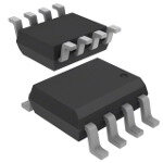
| 供应商器件封装 | 8-SOIC |
| 功率失效检测 | No |
| 包装 | 管件 |
| 受监控电压数 | 1 |
| 商标 | Analog Devices |
| 复位 | 高有效/低有效 |
| 复位超时 | 最小为 250 ms |
| 安装类型 | 表面贴装 |
| 安装风格 | SMD/SMT |
| 封装 | Tube |
| 封装/外壳 | 8-SOIC(0.154",3.90mm 宽) |
| 封装/箱体 | SOIC-8 |
| 工作温度 | -40°C ~ 85°C |
| 工作电源电流 | 50 uA |
| 工厂包装数量 | 98 |
| 最大功率耗散 | 0.9 mW |
| 最大工作温度 | + 85 C |
| 最小工作温度 | - 40 C |
| 标准包装 | 98 |
| 欠电压阈值 | 4.5 V, 4.25 V |
| 电压-阈值 | 可调节/可选择 |
| 电池备用开关 | No Backup |
| 电源电压-最大 | 5.5 V |
| 电源电压-最小 | 4.5 V |
| 监视器 | Watchdog |
| 类型 | Voltage Supervisory |
| 系列 | ADM1232 |
| 芯片启用信号 | No Chip Enable |
| 被监测输入数 | 1 Input |
| 输出 | 开路漏极,推挽式 |
| 输出类型 | Push-Pull |
| 过电压阈值 | 4.74 V, 4.49 V |
| 重置延迟时间 | 1000 ms |
| 阈值电压 | 4.37 V, 4.62 V |


PDF Datasheet 数据手册内容提取
Microprocessor Supervisory Circuit ADM1232 FEATURES FUNCTIONAL BLOCK DIAGRAM Pin-compatible with MAX1232 and Dallas DS1232 Adjustable precision voltage monitor with 4.5 V and TOLERANVCCEC TOS5L%EEL/R1EA0C%NTCE ETATOR RESET 4.75 V options ESER RN Adjustable strobe monitor with 150 ms, 600 ms, or VREF GE RESET 1.2 sec options PB RESET DEBOUNCE No external components Specified from −40°C to +85°C TD WTIAMTEC-BHADSOEG WATTICMHEDROG STROBE SELECT APPLICATIONS GND ADM1232 7522-0010 Microprocessor systems Figure 1. Portable equipment Computers Controllers Intelligent instruments Automotive systems GENERAL DESCRIPTION The ADM1232 is pin-compatible with the MAX1232, DS1232LP, 5V 5V and DS1232. The Analog Devices, Inc., ADM1232 is a micro- 10kΩ processor monitoring circuit that can monitor the following: ADM1232 MICROPROCESSOR • Microprocessor supply voltage STROBE I/O • Whether a microprocessor has locked up RESET RESET • External interrupts GND TD TOLERANCE The ADM1232 is available in four packages: an 8-lead MSOP (RM-8), an 8-lead PDIP (N-8), a 16-lead wide SOIC (RW-16), 07522-002 and an 8-lead narrow SOIC (R-8). Figure 2. Typical Supply Monitoring Application Rev. C Information furnished by Analog Devices is believed to be accurate and reliable. However, no responsibility is assumed by Analog Devices for its use, nor for any infringements of patents or other One Technology Way, P.O. Box 9106, Norwood, MA 02062-9106, U.S.A. rights of third parties that may result from its use. Specifications subject to change without notice. No license is granted by implication or otherwise under any patent or patent rights of Analog Devices. Tel: 781.329.4700 www.analog.com Trademarks and registered trademarks are the property of their respective owners. Fax: 781.461.3113 ©1997–2008 Analog Devices, Inc. All rights reserved.
ADM1232 TABLE OF CONTENTS Features .............................................................................................. 1 Pin Configurations and Function Descriptions ............................5 Applications ....................................................................................... 1 Circuit Information ...........................................................................6 Functional Block Diagram .............................................................. 1 PB RESET .......................................................................................6 General Description ......................................................................... 1 STROBE Timeout Selection .........................................................6 Revision History ............................................................................... 2 Tolerance ........................................................................................6 Specifications ..................................................................................... 3 RESET and RESET Outputs .........................................................6 Absolute Maximum Ratings ............................................................ 4 Outline Dimensions ..........................................................................7 Thermal Resistance ...................................................................... 4 Ordering Guide .............................................................................9 ESD Caution .................................................................................. 4 REVISION HISTORY 12/08—Rev. B to Rev. C Updated Format .................................................................. Universal Changes to Table 2 ............................................................................ 4 Added Thermal Resistance Section ............................................... 4 Updated Outline Dimensions ......................................................... 7 Changes to Ordering Guide ............................................................ 9 12/97—Rev. A to Rev. B Changes to Specifications Section .................................................. 2 x/97—Rev. 0 to Rev. A Changes to Specifications Section .................................................. 2 7/97—Revision 0: Initial Version Rev. C | Page 2 of 12
ADM1232 SPECIFICATIONS V = full operating range, T = T to T , unless otherwise noted. CC A MIN MAX Table 1. Parameter Min Typ Max Unit Test Conditions/Comments TEMPERATURE −40 +85 °C T = T to T . A MIN MAX POWER SUPPLY Voltage 4.5 5.0 5.5 V Current 20 50 μA V , V = CMOS levels. IL IH 200 500 μA V , V = TTL levels. IL IH STROBE AND PB RESET INPUTS Input High Level 2.0 V + 0.3 V CC Input Low Level −0.3 +0.8 V INPUT LEAKAGE CURRENT (STROBE, TOLERANCE) −1.0 +1.0 μA TD 1.6 μA OUTPUT CURRENT RESET 8 10 mA V is at 4.5 V to 5.5 V. CC RESET/RESET −8 −12 mA V is at 4.5 V to 5.5 V. CC OUTPUT VOLTAGE RESET/RESET V − 0.5 V − 0.1 V When sourcing less than 500 μA, RESET remains within CC CC 0.5 V of V on power-down until V drops below 2.0 V. CC CC When sinking less than 500 μA, RESET remains within 0.5 V of GND on power-down until V drops below 2.0 V. CC RESET/RESET High Level 0.4 V RESET/RESET Low Level 2.4 V 1 V OPERATION RESET Output Voltage V − 0.1 V When sourcing less than 50 μA. CC RESET Output Voltage 0.1 V When sinking less than 50 μA. V TRIP POINT CC 5% 4.5 4.62 4.74 V TOLERANCE = GND. 10% 4.25 4.37 4.49 V TOLERANCE = V . CC CAPACITANCE Input (STROBE, TOLERANCE) 5 pF T = 25°C. A Output (RESET, RESET) 7 pF T = 25°C. A PB RESET Time 20 ms PB RESET must be held low for a minimum of 20 ms to guarantee a reset. Delay 1 4 20 ms RESET ACTIVE TIME 250 610 1000 ms STROBE Pulse Width 70 ns Timeout Period 62.5 150 250 ms TD = 0 V. 250 600 1000 ms TD = floating. 500 1200 2000 ms TD = V . CC V CC Fall Time 10 μs Guaranteed by design. Rise Time 0 μs Guaranteed by design. V FAIL DETECT TO RESET RESET and RESET are logically correct. CC OUTPUT DELAY 50 μs After V falls below the set tolerance voltage (see Figure 9). CC 250 610 1000 ms After V rises above the set tolerance voltage. CC Rev. C | Page 3 of 12
ADM1232 ABSOLUTE MAXIMUM RATINGS THERMAL RESISTANCE T = 25°C unless otherwise noted. A θ is specified for the worst-case conditions, that is, a device JA Table 2. soldered in a circuit board for surface-mount packages. Parameter Rating V 5.5 V Table 3. Thermal Resistance CC Logic Inputs −0.3 V to V + 0.3 V Package Type θ Unit CC JA Storage Temperature Range −65°C to +150°C 8-Lead PDIP (N-8) 100 °C/W Lead Temperature (Soldering, 10 sec) 300°C 16-Lead SOIC_W (RW-16) 73 °C/W Vapor Phase (60 sec) 215°C 8-Lead MSOP (RM-8) 206 °C/W Infrared (15 sec) 220°C 8-Lead SOIC_N (R-8) 153 °C/W Power Dissipation N-81 1000 mW ESD CAUTION RW-16, RM-82 900 mW R-82 900 μW 1 Derate by 13.5 mW/°C above 25°C. 2 Derate by 12 mW/°C above 25°C. Stresses above those listed under Absolute Maximum Ratings may cause permanent damage to the device. This is a stress rating only; functional operation of the device at these or any other conditions above those indicated in the operational section of this specification is not implied. Exposure to absolute maximum rating conditions for extended periods may affect device reliability. Rev. C | Page 4 of 12
ADM1232 PIN CONFIGURATIONS AND FUNCTION DESCRIPTIONS NC 1 16 NC PB RESET 2 15 VCC NC 3 ADM1232 14 NC TD 4 TOP VIEW 13 STROBE NC 5 (Not to Scale) 12 NC TOLERANCE 6 11 RESET NC 7 10 NC GND 8NC = NO CONNECT9 RESET 07522-003 Figure 3. RW-16 Pin Configuration PB RESET 1 8 VCC TD 2 ADM1232 7 STROBE TOLERAGNNCDE 34 (NToOt Pto V SIEcaWle) 65 RREESSEETT 07522-004 Figure 4. RM-8 Pin Configuration PB RESET 1 8 VCC TD 2 ADM1232 7 STROBE TOLERAGNNCDE 34 (NToOt Pto V SIEcaWle) 65 RREESSEETT 07522-005 Figure 5. N-8 and R-8 Pin Configuration Table 4. Pin Function Descriptions Pin No. N-8, R-8, RW-16 RM-8 Mnemonic Description 1, 3, 5, 7, NC No Connection. 10, 12, 14, 16 2 1 PB RESET Push-Button Reset Input. This debounced input ignores pulses of less than 1 ms and is guaranteed to respond to pulses greater than 20 ms. 4 2 TD Time Delay Set. This input allows the user to select the maximum amount of time that the ADM1232 allows the STROBE input to remain inactive—that is, STROBE is not receiving any high-to-low transitions—without forcing the ADM1232 to generate a RESET pulse. See the Specifications section, Figure 8, and the STROBE Timeout Selection section. 6 3 TOLERANCE Tolerance Input. This input determines how much the supply voltage is allowed to decrease (as a percentage) before a RESET is asserted. Connect this pin to V for 10% and to GND for 5%. CC 8 4 GND 0 V Ground Reference for All Signals. 9 5 RESET Active High Logic Output. This pin is asserted when any of the following events occurs: V decreases below the amount specified by the TOLERANCE input; when PB RESET is forced low; CC if there are no high-to-low transitions within the limits set by TD at STROBE; and during power-up. 11 6 RESET Inverse of RESET. This pin has an open-drain output. 13 7 STROBE The STROBE input is used to monitor the activity of a microprocessor. If there are no high-to-low transitions within the time specified by TD, a reset is asserted. 15 8 V Power Supply Input, 5 V. CC Rev. C | Page 5 of 12
ADM1232 CIRCUIT INFORMATION PB RESET STROBE TIMEOUT SELECTION The PB RESET input makes it possible to manually reset a TD (time delay) set is used to set the strobe timeout period. The system using either a standard push-button switch or a logic strobe timeout period is the maximum time between high-to- low input. An internal debounce circuit provides glitch low transitions that STROBE accepts before a reset is asserted immunity when used with a switch, reducing the effects of (see Figure 8). The strobe timeout settings are listed in Table 5. glitches on the line. The debounce circuit is guaranteed to cause Table 5. Strobe Timeout Settings the ADM1232 to assert a reset if PB RESET is brought low for Condition Min Typ Max Unit more than 20 ms and is guaranteed to ignore low inputs of less TD = 0 V 62.5 150 250 ms than 1 ms. TD = Floating 250 600 1000 ms VCC TD = V 500 1200 2000 ms CC VCC TD ADM1232 MICROPROCESSOR STROBE PULSE WIDTH STROBE I/O STROBE PB RESET RESET RESET GND TOLERANCE 07522-006 STROBE TIMEOUT PERIOD 07522-008 Figure 6. Typical Push-Button Reset Application Figure 8. STROBE Parameters 5V 5V PB RESET TIME VCC 4.5V (5% TRIP POINT) PB RESET PB RESET 4.25V (10% TRIP POINT) DELAY VIH RESET OUTPUT DELAY RESET OUTPUT DELAY WHEN VCC IS FALLING WHEN VCC IS RISING VIL RESET ACTIVE TIME RESET RESET RESET 07522-009 RESET 0707522-0 TOLERANCE Figure 9. Reset Output Delay Figure 7. PB RESET The TOLERANCE input is used to determine the level at which V can vary below 5 V without the ADM1232 asserting a reset. CC Connecting TOLERANCE to GND selects a −5% tolerance level and causes the ADM1232 to generate a reset if V falls below CC 4.75 V. If TOLERANCE is connected to V , a −10% tolerance CC level is selected, which causes the ADM1232 to generate a reset if V falls below 4.5 V. See the parameters for the V trip point CC CC in the Specifications section for more information. RESET AND RESET OUTPUTS RESET is capable of sourcing and sinking current, whereas RESET is an open-drain MOSFET that sinks current only. Therefore, it is necessary to pull this output high. Rev. C | Page 6 of 12
ADM1232 OUTLINE DIMENSIONS 10.50 (0.4134) 10.10 (0.3976) 16 9 7.60 (0.2992) 7.40 (0.2913) 1 10.65 (0.4193) 8 10.00 (0.3937) 1.27 (0.0500) 0.75 (0.0295) BSC 2.65 (0.1043) 0.25 (0.0098) 45° 0.30 (0.0118) 2.35 (0.0925) 8° 0.10 (0.0039) 0° COPLANARITY 0.10 0.51 (0.0201) SPLEAATNIENG 0.33 (0.0130) 1.27 (0.0500) 0.31 (0.0122) 0.20 (0.0079) 0.40 (0.0157) COMPLIANTTO JEDEC STANDARDS MS-013-AA C(RINOEFNPEATRRREOENNLCLTEIHN EOGSN EDLSIYM)AEANNRDSEI AORRNOESU NANORDEET DAIN-PO MPFRIFLO LMPIIMRLELIATIMTEEER TFSEO; RIRN ECUQHSU EDI VIINMA LEDENENSSTIIOGSN NFS.OR 032707-B Figure 10. 16-Lead Standard Small Outline Package [SOIC_W] Wide Body (RW-16) Dimensions shown in millimeters and (inches) 3.20 3.00 2.80 8 5 5.15 3.20 4.90 3.00 4.65 2.80 1 4 PIN 1 0.65 BSC 0.95 0.85 1.10 MAX 0.75 0.80 0.15 0.38 0.23 8° 0.60 0.00 0.22 0.08 0° 0.40 COPLANARITY SEATING 0.10 PLANE COMPLIANT TO JEDEC STANDARDS MO-187-AA Figure 11. 8-Lead Mini Small Outline Package [MSOP] (RM-8) Dimensions shown in millimeters Rev. C | Page 7 of 12
ADM1232 0.400 (10.16) 0.365 (9.27) 0.355 (9.02) 8 5 0.280 (7.11) 0.250 (6.35) 1 4 0.240 (6.10) 0.325 (8.26) 0.310 (7.87) 0.100 (2.54) 0.300 (7.62) BSC 0.060 (1.52) 0.195 (4.95) 0.210 (5.33) MAX 0.130 (3.30) MAX 0.115 (2.92) 0.015 0.150 (3.81) (0.38) 0.015 (0.38) 0.130 (3.30) MIN GAUGE 0.115 (2.92) SEATING PLANE 0.014 (0.36) PLANE 0.010 (0.25) 0.022 (0.56) 0.008 (0.20) 0.005 (0.13) 0.430 (10.92) 0.018 (0.46) MIN MAX 0.014 (0.36) 0.070 (1.78) 0.060 (1.52) 0.045 (1.14) COMPLIANTTO JEDEC STANDARDS MS-001 CONTROLLING DIMENSIONSARE IN INCHES; MILLIMETER DIMENSIONS (RCINEOFRPEANRERERENN LCTEEHA EODSNSEL MSY)AAAYNR BDEE AR CROOEU NNNFODIGETUDAR-POEPFDRFOA INSPC RWHIAH ETOEQL UFEIO VORAR LU EHSNAETL ISFN FLDOEEARSDIGSN.. 070606-A Figure 12. 8-Lead Plastic Dual In-Line Package [PDIP] Narrow Body (N-8) Dimensions shown in inches and (millimeters) 5.00(0.1968) 4.80(0.1890) 8 5 4.00 (0.1574) 6.20 (0.2441) 3.80 (0.1497) 1 4 5.80 (0.2284) 1.27 (0.0500) 0.50 (0.0196) BSC 1.75 (0.0688) 0.25 (0.0099) 45° 0.25 (0.0098) 1.35 (0.0532) 8° 0.10 (0.0040) 0° COPLANARITY 0.51 (0.0201) 0.10 SEATING 0.31 (0.0122) 0.25 (0.0098) 10..2470 ((00..00510507)) PLANE 0.17 (0.0067) COMPLIANTTO JEDEC STANDARDS MS-012-AA C(RINOEFNPETARRREOENNLCLTEIHN EOGSN DELSIYM)AEANNRDSEI AORRNOESU NANORDEET DAIN-PO MPFRIFLO LMPIIMRLELIATIMTEEER TFSEO; RIRN ECUQHSU EDI VIINMA LEDENENSSTIIOGSN NFS.OR 012407-A Figure 13. 8-Lead Standard Small Outline Package [SOIC_N] Narrow Body (R-8) Dimensions shown in millimeters and (inches) Rev. C | Page 8 of 12
ADM1232 ORDERING GUIDE Temperature Package Model Range Package Description Options Branding ADM1232ARM −40°C to +85°C 8-Lead Mini Small Outline Package [MSOP] RM-8 M2A ADM1232ARM-REEL −40°C to +85°C 8-Lead Mini Small Outline Package [MSOP] RM-8 M2A ADM1232ARM-REEL7 −40°C to +85°C 8-Lead Mini Small Outline Package [MSOP] RM-8 M2A ADM1232ARMZ1 −40°C to +85°C 8-Lead Mini Small Outline Package [MSOP] RM-8 M4W ADM1232ARMZ-REEL1 −40°C to +85°C 8-Lead Mini Small Outline Package [MSOP] RM-8 M4W ADM1232ARMZ-REEL71 −40°C to +85°C 8-Lead Mini Small Outline Package [MSOP] RM-8 M4W ADM1232AN −40°C to +85°C 8-Lead Plastic Dual In-Line Package [PDIP] N-8 ADM1232ANZ1 −40°C to +85°C 8-Lead Plastic Dual In-Line Package [PDIP] N-8 ADM1232ARW −40°C to +85°C 16-Lead Standard Small Outline Package [SOIC_W], Wide Body RW-16 ADM1232ARW-REEL −40°C to +85°C 16-Lead Standard Small Outline Package [SOIC_W], Wide Body RW-16 ADM1232ARW-REEL7 −40°C to +85°C 16-Lead Standard Small Outline Package [SOIC_W], Wide Body RW-16 ADM1232ARWZ1 −40°C to +85°C 16-Lead Standard Small Outline Package [SOIC_W], Wide Body RW-16 ADM1232ARWZ-REEL1 −40°C to +85°C 16-Lead Standard Small Outline Package [SOIC_W], Wide Body RW-16 ADM1232ARWZ-REEL71 −40°C to +85°C 16-Lead Standard Small Outline Package [SOIC_W], Wide Body RW-16 ADM1232ARN −40°C to +85°C 8-Lead Standard Small Outline Package [SOIC_N] R-8 ADM1232ARN-REEL −40°C to +85°C 8-Lead Standard Small Outline Package [SOIC_N] R-8 ADM1232ARN-REEL7 −40°C to +85°C 8-Lead Standard Small Outline Package [SOIC_N] R-8 ADM1232ARNZ1 −40°C to +85°C 8-Lead Standard Small Outline Package [SOIC_N] R-8 ADM1232ARNZ-REEL1 −40°C to +85°C 8-Lead Standard Small Outline Package [SOIC_N] R-8 ADM1232ARNZ-REEL71 −40°C to +85°C 8-Lead Standard Small Outline Package [SOIC_N] R-8 1 Z = RoHS Compliant Part. Rev. C | Page 9 of 12
ADM1232 NOTES Rev. C | Page 10 of 12
ADM1232 NOTES Rev. C | Page 11 of 12
ADM1232 NOTES ©1997–2008 Analog Devices, Inc. All rights reserved. Trademarks and registered trademarks are the property of their respective owners. D07522-0-12/08(C) Rev. C | Page 12 of 12