ICGOO在线商城 > 集成电路(IC) > PMIC - 监控器 > ADM1063ACPZ
 Datasheet下载
- 型号: ADM1063ACPZ
- 制造商: Analog
- 库位|库存: xxxx|xxxx
- 要求:
| 数量阶梯 | 香港交货 | 国内含税 |
| +xxxx | $xxxx | ¥xxxx |
查看当月历史价格
查看今年历史价格
ADM1063ACPZ产品简介:
ICGOO电子元器件商城为您提供ADM1063ACPZ由Analog设计生产,在icgoo商城现货销售,并且可以通过原厂、代理商等渠道进行代购。 ADM1063ACPZ价格参考。AnalogADM1063ACPZ封装/规格:PMIC - 监控器, 可编程 监控器 10 通道 40-LFCSP-VQ(6x6)。您可以下载ADM1063ACPZ参考资料、Datasheet数据手册功能说明书,资料中有ADM1063ACPZ 详细功能的应用电路图电压和使用方法及教程。
| 参数 | 数值 |
| 产品目录 | 集成电路 (IC)半导体 |
| 描述 | IC SEQUENCER/SUPERVISOR 40LFCSP监控电路 Multisupply Supvsr Sequencer w/ ADC |
| 产品分类 | |
| 品牌 | Analog Devices Inc |
| 产品手册 | |
| 产品图片 |
|
| rohs | 符合RoHS无铅 / 符合限制有害物质指令(RoHS)规范要求 |
| 产品系列 | 电源管理 IC,监控电路,Analog Devices ADM1063ACPZSuper Sequencer® |
| NumberofInputsMonitored | 10 Input |
| 数据手册 | |
| 产品型号 | ADM1063ACPZ |
| PCN组件/产地 | |
| 产品种类 | 监控电路 |
| 人工复位 | Manual Reset |
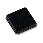
| 供应商器件封装 | 40-LFCSP-VQ(6x6) |
| 包装 | 托盘 |
| 受监控电压数 | 10 |
| 商标 | Analog Devices |
| 复位 | - |
| 复位超时 | - |
| 安装类型 | 表面贴装 |
| 安装风格 | SMD/SMT |
| 封装 | Tray |
| 封装/外壳 | 40-VFQFN 裸露焊盘,CSP |
| 封装/箱体 | LFCSP-40 |
| 工作温度 | -40°C ~ 85°C |
| 工作电源电流 | 4.2 mA |
| 工厂包装数量 | 490 |
| 最大工作温度 | + 85 C |
| 最小工作温度 | - 40 C |
| 标准包装 | 1 |
| 欠电压阈值 | 0.573 V, 1.25 V, 2.5 V, 6 V |
| 电压-阈值 | 可调节/可选择 |
| 电池备用开关 | No Backup |
| 电源电压-最大 | 5.4 V, 14.4 V |
| 电源电压-最小 | 2.7 V, 3 V |
| 监视器 | Watchdog |
| 类型 | 序列发生器 |
| 系列 | ADM1063 |
| 芯片启用信号 | Chip Enable |
| 被监测输入数 | 10 Input |
| 输出 | 可编程 |
| 输出类型 | Open Collector / Drain & Push-Pull |
| 过电压阈值 | 0.8 V, 1.75 V, 3.5 V, 8.4 V |
| 配用 | /product-detail/zh/EVAL-ADM1063TQEBZ/EVAL-ADM1063TQEBZ-ND/1534685 |
| 阈值电压 | 0.573 V to 1.375 V, 1.25 V to 3 V, 2.5 V to 6 V, 6 V to 14.4 V |


- 商务部:美国ITC正式对集成电路等产品启动337调查
- 曝三星4nm工艺存在良率问题 高通将骁龙8 Gen1或转产台积电
- 太阳诱电将投资9.5亿元在常州建新厂生产MLCC 预计2023年完工
- 英特尔发布欧洲新工厂建设计划 深化IDM 2.0 战略
- 台积电先进制程称霸业界 有大客户加持明年业绩稳了
- 达到5530亿美元!SIA预计今年全球半导体销售额将创下新高
- 英特尔拟将自动驾驶子公司Mobileye上市 估值或超500亿美元
- 三星加码芯片和SET,合并消费电子和移动部门,撤换高东真等 CEO
- 三星电子宣布重大人事变动 还合并消费电子和移动部门
- 海关总署:前11个月进口集成电路产品价值2.52万亿元 增长14.8%


PDF Datasheet 数据手册内容提取
Multisupply Supervisor/Sequencer with ADC and Temperature Monitoring Data Sheet ADM1063-EP FEATURES FUNCTIONAL BLOCK DIAGRAM Complete supervisory and sequencing solution for up to D1PD1ND2PD2N REFIN REFOUT REFGND SDA SCL A1 A0 10 supplies Extended temperature range: −40°C to +105°C TEMP INTERNAL VREF SMBus SENSOR DIODE INTERFACE 10 supply fault detectors enable supervision of supplies to <0.5% accuracy at all voltages at 25°C X U <1.0% accuracy across all voltages and temperatures M 12-BIT SARADC EEPROM 5 selectable input attenuators allow supervision of supplies to CLOSED-LOOP 14.4 V on VH MARGINING SYSTEM 6 V on VP1 to VP4 (VPx) VX1 DUAL- CONFIGURABLE PDO1 VX2 FUNCTION OUTPUT PDO2 5 dual-function inputs, VX1 to VX5 (VXx) INPUTS DRIVERS PDO3 VX3 High impedance input to supply fault detector with VX4 (LOGICO RINPUTS (DHRV ICVIANPGA BGLAET EOSF PPDDOO45 thresholds between 0.573 V and 1.375 V VX5 SFDs) OF N-FET) PDO6 SEQUENCING General-purpose logic input ENGINE VP1 CONFIGURABLE PDO7 10 programmable driver outputs, PDO1 to PDO10 (PDOx) VP2 PROGRAMMABLE OUTPUT RESET DRIVERS PDO8 Open-collector with external pull-up VP3 GENERATORS (LV CAPABLE PDO9 Push/pull output, driven to VDDCAP or VPx VP4 (SFDs) OF DRIVING Open collector with weak pull-up to VDDCAP or VPx VH LOGIC SIGNALS) PDO10 AGND PDOGND Internally charge-pumped high drive for use with external N-FET (PDO1 to PDO6 only) ADM1063-EP ARBIVTDRDATOR VDDCAP SePqDueOnxc oinugt peuntgsi ne (SE) implements state machine control of VCCP GND 09116-001 State changes conditional on input events Figure 1. Enables complex control of boards Power-up and power-down sequence control Fault event handling APPLICATIONS Interrupt generation on warnings Central office systems Watchdog function can be integrated in SE Servers/routers Program software control of sequencing through SMBus Multivoltage system line cards Complete voltage margining solution for 6 voltage rails DSP/FPGA supply sequencing 12-bit ADC for readback of all supervised voltages In-circuit testing of margined supplies 1 internal and 2 external temperature sensors Reference input (REFIN) has 2 input options GENERAL DESCRIPTION Driven directly from 2.048 V (±0.25%) REFOUT pin The ADM1063-EP is a configurable supervisory/sequencing More accurate external reference for improved ADC device that offers a single-chip solution for supply monitoring performance and sequencing in multiple supply systems. In addition to these Device powered by the highest of VPx, VH for improved functions, the ADM1063-EP integrates a 12-bit ADC that can redundancy be used to accurately read back up to 12 separate voltages. User EEPROM: 256 bytes The device also provides up to 10 programmable inputs for Industry-standard, 2-wire bus interface (SMBus) monitoring undervoltage faults, overvoltage faults, or out-of- Guaranteed PDO low with VH, VPx = 1.2 V window faults on up to 10 supplies. In addition, 10 programmable Available in 40-lead, 6 mm × 6 mm LFCSP package outputs can be used as logic enables. Six of these programmable outputs can provide up to a 12 V output for driving the gate of For more information about the ADM1063 register map, an N-FET that can be placed in the path of a supply. refer to the AN-698 Application Note at www.analog.com. Rev. A Document Feedback Information furnished by Analog Devices is believed to be accurate and reliable. However, no responsibility is assumed by Analog Devices for its use, nor for any infringements of patents or other One Technology Way, P.O. Box 9106, Norwood, MA 02062-9106, U.S.A. rights of third parties that may result from its use. Specifications subject to change without notice. No license is granted by implication or otherwise under any patent or patent rights of Analog Devices. Tel: 781.329.4700 ©2010–2013 Analog Devices, Inc. All rights reserved. Trademarks and registered trademarks are the property of their respective owners. Technical Support www.analog.com
ADM1063-EP Data Sheet TABLE OF CONTENTS Features .............................................................................................. 1 Thermal Resistance .......................................................................7 Functional Block Diagram .............................................................. 1 ESD Caution...................................................................................7 Applications ....................................................................................... 1 Pin Configuration and Function Descriptions ..............................8 General Description ......................................................................... 1 Typical Performance Characteristics ..............................................9 Revision History ............................................................................... 2 Outline Dimensions ....................................................................... 12 Detailed Block Diagram .................................................................. 3 Ordering Guide .......................................................................... 12 Specifications ..................................................................................... 4 Absolute Maximum Ratings ............................................................ 7 REVISION HISTORY 8/13—Rev. 0 to Rev. A Changes to Serial Bus Timing Parameters; Table 1 ...................... 6 Updated Outline Dimensions ....................................................... 12 5/10—Revision 0: Initial Version Rev. A | Page 2 of 12
Data Sheet ADM1063-EP Temperature measurement is possible with the ADM1063-EP. The device is controlled via configuration data that can be The device contains one internal temperature sensor and two programmed into an EEPROM. The entire configuration can pairs of differential inputs for remote thermal diodes. These are be programmed using an intuitive GUI-based software package measured by the 12-bit ADC. provided by Analog Devices, Inc. The logical core of the device is a sequencing engine. This state- Full details about this enhanced product are available in the machine-based construction provides up to 63 different states. ADM1063 data sheet, which should be consulted in conjunction This design enables very flexible sequencing of the outputs with this data sheet. based on the condition of the inputs. DETAILED BLOCK DIAGRAM REFIN REFOUT D1P D1N D2P D2N REFGND SDA SCL A1 A0 ADM1063-EP TEMP INTERNAL SENSOR DIODE VREF SMBus INTERFACE OSC 12-BIT DEVICE SAR ADC CONTROLLER EEPROM GPI SIGNAL CONFIGURABLE CONDITIONING OUTPUT DRIVER PDO1 (HV) VX1 SFD PDO2 VX2 PDO3 VX3 PDO4 VX4 PDO5 GPI SIGNAL CONDITIONING OCOUTNPFUIGTU DRRAIBVELER PDO6 SEQUENCING (HV) VX5 ENGINE SFD VP1 ASTETLEENCUTAATBOLER SFD OCOUTNPFUIGTU DRRAIBVELER PDO7 (LV) VP2 VP3 PDO8 VP4 PDO9 VH ASTETLEENCUTAATBOLER SFD OCOUTNPFUIGTU DRRAIBVELER PDO10 (LV) AGND PDOGND REG 5.25V VDDCAP VDD CHARGE PUMP ARBITRATOR GND VCCP 09116-002 Figure 2. Rev. A | Page 3 of 12
ADM1063-EP Data Sheet SPECIFICATIONS VH = 3.0 V to 14.4 V1, VPx = 3.0 V to 6.0 V1, T = −40°C to +105°C, unless otherwise noted. A Table 1. Parameter Min Typ Max Unit Test Conditions/Comments POWER SUPPLY ARBITRATION VH, VPx 3.0 V Minimum supply required on one of VH, VPx VPx 6.0 V Maximum VDDCAP = 5.1 V, typical VH 14.4 V VDDCAP = 4.75 V VDDCAP 2.7 4.75 5.4 V Regulated LDO output C 10 µF Minimum recommended decoupling capacitance VDDCAP POWER SUPPLY Supply Current, I , I 4.2 6 mA VDDCAP = 4.75 V, PDO1 to PDO10 off, ADC off VH VPx Additional Currents All PDO FET Drivers On 1 mA VDDCAP = 4.75 V, PDO1 to PDO6 loaded with 1 µA each, PDO7 to PDO10 off Current Available from VDDCAP 2 mA Maximum additional load that can be drawn from all PDO pull-ups to VDDCAP ADC Supply Current 1 mA Running round-robin loop EEPROM Erase Current 10 mA 1 ms duration only, VDDCAP = 3 V SUPPLY FAULT DETECTORS VH Pin Input Impedance 52 kΩ Input Attenuator Error ±0.05 % Midrange and high range Detection Ranges High Range 6 14.4 V Midrange 2.5 6 V VPx Pins Input Impedance 52 kΩ Input Attenuator Error ±0.05 % Low range and midrange Detection Ranges Midrange 2.5 6 V Low Range 1.25 3 V Ultralow Range 0.573 1.375 V No input attenuation error VXx Pins Input Impedance 1 MΩ Detection Range Ultralow Range 0.573 1.375 V No input attenuation error Absolute Accuracy ±1 % VREF error + DAC nonlinearity + comparator offset error + input attenuation error Threshold Resolution 8 Bits Digital Glitch Filter 0 µs Minimum programmable filter length 100 µs Maximum programmable filter length Rev. A | Page 4 of 12
Data Sheet ADM1063-EP Parameter Min Typ Max Unit Test Conditions/Comments ANALOG-TO-DIGITAL CONVERTER Signal Range 0 V V The ADC can convert signals presented to the VH, REFIN VPx, and VXx pins; VPx and VH input signals are attenuated depending on the selected range; a signal at the pin corresponding to the selected range is from 0.573 V to 1.375 V at the ADC input Input Reference Voltage on REFIN Pin, V 2.048 V REFIN Resolution 12 Bits INL ±2.5 LSB Endpoint corrected, V = 2.048 V REFIN Gain Error ±0.05 % V = 2.048 V REFIN Conversion Time 0.44 ms One conversion on one channel 84 ms All 12 channels selected, 16× averaging enabled Offset Error ±2 LSB V = 2.048 V REFIN Input Noise 0.25 LSB rms Direct input (no attenuator) TEMPERATURE SENSOR2 Local Sensor Accuracy ±3 °C VDDCAP = 4.75 V Local Sensor Supply Voltage Coefficient −1.7 °C/V Remote Sensor Accuracy ±3 °C VDDCAP = 4.75 V Remote Sensor Supply Voltage Coefficient −3 °C Remote Sensor Current Source 200 µA High level 12 µA Low level Temperature for Code 0x800 0 °C VDDCAP = 4.75 V Temperature for Code 0xC00 128 °C VDDCAP = 4.75 V Temperature Resolution per Code 0.125 °C REFERENCE OUTPUT Reference Output Voltage 2.043 2.048 2.053 V No load Load Regulation −0.25 mV Sourcing current, I = −100 µA DACxMAX 0.25 mV Sinking current, I = 100 µA DACxMAX Minimum Load Capacitance 1 µF Capacitor required for decoupling, stability PSRR 60 dB DC PROGRAMMABLE DRIVER OUTPUTS High Voltage (Charge Pump) Mode (PDO1 to PDO6) Output Impedance 500 kΩ V 11 12.5 14 V I = 0 µA OH OH 10.5 12 13.5 V I = 1 µA OH I 20 µA 2 V < V < 7 V OUTAVG OH Standard (Digital Output) Mode (PDO1 to PDO10) V 2.4 V V (pull-up to VDDCAP or VPx) = 2.7 V, I = 0.5 mA OH PU OH 4.5 V V to VPx = 6.0 V, I = 0 mA PU OH V − 0.3 V V ≤ 2.7 V, I = 0.5 mA PU PU OH V 0 0.50 V I = 20 mA OL OL I 3 20 mA Maximum sink current per PDOx pin OL I 3 60 mA Maximum total sink for all PDOx pins SINK R 19 20 29 kΩ Internal pull-up PULL-UP I (VPx)3 2 mA Current load on any VPx pull-ups, that is, total source SOURCE current available through any number of PDOx pull-up switches configured onto any one VPx pin Three-State Output Leakage Current 10 µA V = 14.4 V PDO Oscillator Frequency 90 100 110 kHz All on-chip time delays derived from this clock Rev. A | Page 5 of 12
ADM1063-EP Data Sheet Parameter Min Typ Max Unit Test Conditions/Comments DIGITAL INPUTS (VXx, A0, A1) Input High Voltage, V 2.0 V Maximum V = 5.5 V IH IN Input Low Voltage, V 0.8 V Maximum V = 5.5 V IL IN Input High Current, I −1 µA V = 5.5 V IH IN Input Low Current, I 1 µA V = 0 V IL IN Input Capacitance 5 pF Programmable Pull-Down Current, 20 µA VDDCAP = 4.75 V, T = 25°C if known logic state A I is required PULL-DOWN SERIAL BUS DIGITAL INPUTS (SDA, SCL) Input High Voltage, V 2.0 V IH Input Low Voltage, V 0.8 V IL Output Low Voltage, V 3 0.4 V I = −3.0 mA OL OUT SERIAL BUS TIMING4 Clock Frequency, f 400 kHz SCLK Bus Free Time, t 1.3 µs BUF Start Setup Time, t 0.6 µs SU;STA Stop Setup Time, t 0.6 µs SU;STO Start Hold Time, t 0.6 µs HD;STA SCL Low Time, t 1.3 µs LOW SCL High Time, t 0.6 µs HIGH SCL, SDA Rise Time, t 300 ns R SCL, SDA Fall Time, t 300 ns F Data Setup Time, t 100 ns SU;DAT Data Hold Time, t 5 ns HD;DAT Input Low Current, I 1 µA V = 0 V IL IN SEQUENCING ENGINE TIMING State Change Time 10 µs 1 At least one of the VH, VPx pins must be ≥3.0 V to maintain the device supply on VDDCAP. 2 All temperature sensor measurements are taken with round-robin loop enabled and at least one other voltage input being measured. 3 Specification is not production tested but is supported by characterization data at initial product release. 4 Timing specifications are guaranteed by design and supported by characterization data. Rev. A | Page 6 of 12
Data Sheet ADM1063-EP ABSOLUTE MAXIMUM RATINGS THERMAL RESISTANCE Table 2. θ is specified for the worst-case conditions, that is, a device Parameter Rating JA soldered in a circuit board for surface-mount packages. Voltage on VH Pin 16 V Voltage on VPx Pins 7 V Table 3. Thermal Resistance Voltage on VXx Pins −0.3 V to +6.5 V Package Type θ Unit JA Voltage on A0, A1 Pins −0.3 V to +7 V 40-Lead LFCSP 26.5 °C/W Voltage on REFIN, REFOUT Pins 5 V Voltage on VDDCAP, VCCP Pins 6.5 V Voltage on PDOx Pins 16 V ESD CAUTION Voltage on SDA, SCL Pins 7 V Voltage on GND, AGND, PDOGND, REFGND Pins −0.3 V to +0.3 V Voltage on DxN, DxP Pins −0.3 V to +5 V Input Current at Any Pin ±5 mA Package Input Current ±20 mA Maximum Junction Temperature (T max) 150°C J Storage Temperature Range −65°C to +150°C Lead Temperature 215°C (Soldering Vapor Phase, 60 sec) ESD Rating, All Pins 2000 V Stresses above those listed under Absolute Maximum Ratings may cause permanent damage to the device. This is a stress rating only; functional operation of the device at these or any other conditions above those indicated in the operational section of this specification is not implied. Exposure to absolute maximum rating conditions for extended periods may affect device reliability. Rev. A | Page 7 of 12
ADM1063-EP Data Sheet PIN CONFIGURATION AND FUNCTION DESCRIPTIONS P D A N C P G GND VDD D1P D1N D2P D2N A1 A0 VCC PDO 40 39 38 37 36 35 34 33 32 31 VX1 1 30 PDO1 PIN 1 VX2 2 INDICATOR 29 PDO2 VX3 3 28 PDO3 VX4 4 27 PDO4 ADM1063-EP VX5 5 26 PDO5 TOP VIEW VP1 6 (Not to Scale) 25 PDO6 VP2 7 24 PDO7 VP3 8 23 PDO8 VP4 9 22 PDO9 VH 10 21 PDO10 11 12 13 14 15 16 17 18 19 20 D D N T C C L A C C AGN EFGN REFI EFOU N N SC SD N N NC = NO CONNERCT R 09116-003 Figure 3. Pin Configuration Table 4. Pin Function Descriptions Pin No. Mnemonic 1 to 5 VX1 to VX5 (VXx) 6 to 9 VP1 to VP4 (VPx) 10 VH 11 AGND (In a typical application, all ground pins are connected together.) 12 REFGND (In a typical application, all ground pins are connected together.) 13 REFIN 14 REFOUT 15, 16, 19, 20 NC 17 SCL 18 SDA 21 to 30 PDO10 to PDO1 31 PDOGND (In a typical application, all ground pins are connected together.) 32 VCCP 33 A0 34 A1 35 D2N 36 D2P 37 D1N 38 D1P 39 VDDCAP 40 GND (In a typical application, all ground pins are connected together.) EPAD Exposed pad. This pad is a no connect (NC). If possible, this pad should be soldered to the board for improved mechanical stability. Rev. A | Page 8 of 12
Data Sheet ADM1063-EP TYPICAL PERFORMANCE CHARACTERISTICS 6 180 160 5 140 4 120 V) V (VDDCAP 3 I (µA)VP110800 2 60 40 1 20 00 1 2 VVP31 (V) 4 5 6 09116-050 00 1 2 VVP31 (V) 4 5 6 09116-053 Figure 4. VVDDCAP vs. VVP1 Figure 7. IVP1 vs. VVP1 (VP1 Not as Supply) 6 5.0 4.5 5 4.0 3.5 4 V) 3.0 (DCAP 3 (mA)H 2.5 D V VV I 2.0 2 1.5 1.0 1 0.5 00 2 4 6 VVH8 (V) 10 12 14 16 09116-051 00 2 4 6 VVH8 (V) 10 12 14 16 09116-054 Figure 5. VVDDCAP vs. VVH Figure 8. IVH vs. VVH (VH as Supply) 5.0 350 4.5 300 4.0 3.5 250 3.0 I (mA)VP1 22..50 I (µA)VH210500 1.5 100 1.0 50 0.5 00 1 2 VVP31 (V) 4 5 6 09116-052 00 1 2 VVH3 (V) 4 5 6 09116-055 Figure 6. IVP1 vs. VVP1 (VP1 as Supply) Figure 9. IVH vs. VVH (VH Not as Supply) Rev. A | Page 9 of 12
ADM1063-EP Data Sheet 14 1.0 0.8 12 0.6 V) (O1 10 0.4 D P D V 8 B) 0.2 E S E-PUMP 6 DNL (L –0.20 G AR 4 –0.4 H C –0.6 2 –0.8 00 2.5 5.0 ILOA7D.5 (µA) 10.0 12.5 15.0 09116-056 –1.00 1000 2C0O0D0E 3000 4000 09116-066 Figure 10. Charge-Pumped VPDO1 (FET Drive Mode) vs. ILOAD Figure 13. DNL for ADC 5.0 1.0 4.5 0.8 4.0 0.6 3.5 0.4 3.0 0.2 V (V)PDO1 22..50 VP1 = 3V VP1 = 5V INL (LSB)–0.20 1.5 –0.4 1.0 –0.6 0.5 –0.8 00 1 2 ILOAD3 (mA) 4 5 6 09116-057 –1.00 1000 C2O00D0E 3000 4000 09116-063 Figure 11. VPDO1 (Strong Pull-Up to VPx) vs. ILOAD Figure 14. INL for ADC 4.5 12000 4.0 9894 10000 3.5 VP1 = 5V 3.0 8000 E D V) 2.5 CO (O1 VP1 = 3V ER 6000 VPD 2.0 S P T 1.5 HI4000 1.0 2000 0.5 25 81 00 10 20 ILOA3D0(µA) 40 50 60 09116-058 0 2047 C2O0D48E 2049 09116-064 Figure 12. VPDO1 (Weak Pull-Up to VPx) vs. ILOAD Figure 15. ADC Noise, Midcode Input, 10,000 Reads Rev. A | Page 10 of 12
Data Sheet ADM1063-EP 2.058 2.053 V) VP1 = 3.0V T ( U 2.048 O F RE VP1 = 4.75V 2.043 2.038–40 –20 0 TEM2P0ERATUR4E0 (°C) 60 80 100 09116-061 Figure 16. REFOUT vs. Temperature Rev. A | Page 11 of 12
ADM1063-EP Data Sheet OUTLINE DIMENSIONS 6.10 0.30 6.00 SQ 0.25 PIN 1 5.90 0.18 INDICATOR PIN 1 31 40 INDICATOR 30 1 0.50 BSC EXPOSED 4.25 PAD 4.10 SQ 3.95 21 10 TOP VIEW 00..4450 20 BOTTOM VIEW 11 0.25 MIN 0.35 FOR PROPER CONNECTION OF 0.80 THE EXPOSED PAD, REFER TO 0.75 THE PIN CONFIGURATION AND 0.05 MAX FUNCTION DESCRIPTIONS 0.70 0.02 NOM SECTION OF THIS DATA SHEET. COPLANARITY 0.08 SEPALTAINNGE COMPLIANT TO JED0.E2C0 RSTEAFNDARDS MO-220-WJJD. 05-06-2011-A Figure 17. 40-Lead Lead Frame Chip Scale Package [LFCSP_WQ] 6 mm × 6 mm Body, Very Thin Quad (CP-40-9) Dimensions shown in millimeters ORDERING GUIDE Model1 Temperature Range Package Description Package Option ADM1063BCPZ-EP-RL7 −40°C to +105°C 40-Lead LFCSP_WQ CP-40-9 1 Z = RoHS Compliant Part. ©2010–2013 Analog Devices, Inc. All rights reserved. Trademarks and registered trademarks are the property of their respective owners. D09116-0-8/13(A) Rev. A | Page 12 of 12
Mouser Electronics Authorized Distributor Click to View Pricing, Inventory, Delivery & Lifecycle Information: A nalog Devices Inc.: ADM1063ACPZ ADM1063ACPZ-REEL7 ADM1063ASUZ ADM1063ASUZ-REEL7 EVAL-ADM1063TQEBZ