ICGOO在线商城 > 射频/IF 和 RFID > RF 检测器 > ADL5501AKSZ-R7
 Datasheet下载
- 型号: ADL5501AKSZ-R7
- 制造商: Analog
- 库位|库存: xxxx|xxxx
- 要求:
| 数量阶梯 | 香港交货 | 国内含税 |
| +xxxx | $xxxx | ¥xxxx |
查看当月历史价格
查看今年历史价格
ADL5501AKSZ-R7产品简介:
ICGOO电子元器件商城为您提供ADL5501AKSZ-R7由Analog设计生产,在icgoo商城现货销售,并且可以通过原厂、代理商等渠道进行代购。 ADL5501AKSZ-R7价格参考。AnalogADL5501AKSZ-R7封装/规格:RF 检测器, RF Detector IC General Purpose 50MHz ~ 6GHz -18dBm ~ 6dBm ±1dB 6-TSSOP, SC-88, SOT-363。您可以下载ADL5501AKSZ-R7参考资料、Datasheet数据手册功能说明书,资料中有ADL5501AKSZ-R7 详细功能的应用电路图电压和使用方法及教程。
| 参数 | 数值 |
| 产品目录 | |
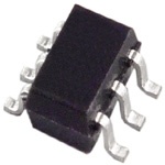
| 描述 | IC DETECTOR RF/IF TRUPWR SC70-6射频检测器 Pwr RMS Detector 50MHz - 4GHz |
| 产品分类 | |
| 品牌 | Analog Devices Inc |
| 产品手册 | |
| 产品图片 |
|
| rohs | 符合RoHS无铅 / 符合限制有害物质指令(RoHS)规范要求 |
| 产品系列 | RF集成电路,射频检测器,Analog Devices ADL5501AKSZ-R7- |
| 数据手册 | |
| 产品型号 | ADL5501AKSZ-R7 |
| RF类型 | 通用 |
| 产品培训模块 | http://www.digikey.cn/PTM/IndividualPTM.page?site=cn&lang=zhs&ptm=25139 |
| 产品目录页面 | |
| 产品种类 | 射频检测器 |
| 其它名称 | ADL5501AKSZ-R7CT |
| 包装 | 剪切带 (CT) |
| 商标 | Analog Devices |
| 安装风格 | SMD/SMT |
| 封装 | Reel |
| 封装/外壳 | 6-TSSOP,SC-88,SOT-363 |
| 封装/箱体 | SC70-6 |
| 工厂包装数量 | 3000 |
| 最大工作温度 | + 85 C |
| 最大正向电压 | 2.7 V to 5.5 V |
| 最小工作温度 | - 40 C |
| 标准包装 | 1 |
| 电压-电源 | 2.7 V ~ 5.5 V |
| 电流-电源 | 1.1mA |
| 精度 | ±1dB |
| 系列 | ADL5501 |
| 视频文件 | http://www.digikey.cn/classic/video.aspx?PlayerID=1364138032001&width=640&height=505&videoID=2245193150001 |
| 输入范围 | -18dBm ~ 6dBm |
| 频率 | 50MHz ~ 6GHz |
| 频率范围 | 6000 MHz |


- 商务部:美国ITC正式对集成电路等产品启动337调查
- 曝三星4nm工艺存在良率问题 高通将骁龙8 Gen1或转产台积电
- 太阳诱电将投资9.5亿元在常州建新厂生产MLCC 预计2023年完工
- 英特尔发布欧洲新工厂建设计划 深化IDM 2.0 战略
- 台积电先进制程称霸业界 有大客户加持明年业绩稳了
- 达到5530亿美元!SIA预计今年全球半导体销售额将创下新高
- 英特尔拟将自动驾驶子公司Mobileye上市 估值或超500亿美元
- 三星加码芯片和SET,合并消费电子和移动部门,撤换高东真等 CEO
- 三星电子宣布重大人事变动 还合并消费电子和移动部门
- 海关总署:前11个月进口集成电路产品价值2.52万亿元 增长14.8%


PDF Datasheet 数据手册内容提取
50 MHz to 6 GHz TruPwr Detector ADL5501 FEATURES 5 True rms response Excellent temperature stability Up to 30 dB input dynamic range 1 50 Ω input impedance V) 1.25 V rms, 15 dBm, maximum input T ( U Single-supply operation: 2.7 V to 5.5 V TP U Low power: 3.3 mW at 3 V supply O RoHS-compliant 0.1 APPLICATIONS Measurement of CDMA-, CDMA2000-, W-CDMA-, and QPSK-/ 0.03 QwAavMe-fboarmsesd OFDM, and other complex modulation –25 –20 –15 –10INPUT– 5(dBm)0 5 10 15 06056-001 Figure 1. Output vs. Input Level, Supply = 3 V, Frequency = 1.9 GHz RF transmitter or receiver power measurement GENERAL DESCRIPTION The ADL5501 is a mean-responding TruPwr™ power detector The on-chip, 100 Ω series resistance at the output, combined for use in high frequency receiver and transmitter signal chains with an external shunt capacitor, creates a low-pass filter response from 50 MHz to 6 GHz. It is easy to apply, requiring only a single that reduces the residual ripple in the dc output voltage. For more supply between 2.7 V and 5.5 V and a power supply decoupling complex waveforms, an external capacitor at the FLTR pin can capacitor. The input is internally ac-coupled and has a nominal be used for supplementary signal demodulation. input impedance of 50 Ω. The output is a linear-responding dc The ADL5501 offers excellent temperature stability across a voltage with a conversion gain of 6.3 V/V rms at 900 MHz. 30 dB range and near 0 dB measurement error across temperature The ADL5501 is intended for true power measurement of simple over the top portion of the dynamic range. In addition to its and complex waveforms. The device is particularly useful for temperature stability, the ADL5501 offers low process variations measuring high crest factor (high peak-to-rms ratio) signals, that further reduce calibration complexity. such as CDMA-, CDMA2000-, W-CDMA-, and QPSK-/QAM- The ADL5501 operates from −40°C to +85°C and is available in based OFDM waveforms. The on-chip modulation filter provides a small 6-lead SC-70 package. It is fabricated on a proprietary adequate averaging for most waveforms. high f silicon bipolar process. T FUNCTIONAL BLOCK DIAGRAM ADL5501 VPOS INTERNAL FILTER i CAPACITOR RFIN x2 FLTR TRANS- CONDICTANCE CELLS ERROR AMP i x2 BUFFER VRMS 100Ω BAND-GAP REFERENCE ENBL COMM 06056-002 Figure 2. Rev. B Information furnished by Analog Devices is believed to be accurate and reliable. However, no responsibility is assumed by Analog Devices for its use, nor for any infringements of patents or other One Technology Way, P.O. Box 9106, Norwood, MA 02062-9106, U.S.A. rights of third parties that may result from its use. Specifications subject to change without notice. No license is granted by implication or otherwise under any patent or patent rights of Analog Devices. Tel: 781.329.4700 www.analog.com Trademarks and registered trademarks are the property of their respective owners. Fax: 781.461.3113 ©2006–2009 Analog Devices, Inc. All rights reserved.
ADL5501 TABLE OF CONTENTS Features .............................................................................................. 1 Input Coupling Using a Series Resistor ................................... 19 Applications ....................................................................................... 1 Multiple RF Inputs ..................................................................... 19 General Description ......................................................................... 1 Selecting the Square-Domain Filter and Output Low-Pass Functional Block Diagram .............................................................. 1 Filter ............................................................................................. 19 Revision History ............................................................................... 2 Power Consumption, Enable, and Power-On/Power-Off Response Time ............................................................................ 20 Specifications ..................................................................................... 3 Output Drive Capability and Buffering ................................... 21 Absolute Maximum Ratings ............................................................ 9 VRMS Output Offset ................................................................. 21 ESD Caution .................................................................................. 9 Device Calibration and Error Calculation .............................. 22 Pin Configuration and Function Descriptions ........................... 10 Calibration for Improved Accuracy ......................................... 22 Typical Performance Characteristics ........................................... 11 Drift over a Reduced Temperature Range .............................. 23 Circuit Description ......................................................................... 17 Operation Below 100 MHz ....................................................... 23 Filtering ........................................................................................ 17 Evaluation Board ........................................................................ 23 Applications Information .............................................................. 18 Outline Dimensions ....................................................................... 25 Basic Connections ...................................................................... 18 Ordering Guide .......................................................................... 25 Output Swing .............................................................................. 18 Linearity ....................................................................................... 18 REVISION HISTORY 3/09—Rev. A to Rev. B 10/07—Rev. 0 to Rev. A Change to Features ........................................................................... 1 Changes to General Description ..................................................... 1 Changes to Table 1 ............................................................................ 3 Changes to Table 1 ............................................................................. 3 Changes to Figure 4, Figure 5, Figure 7, and Figure 9 ............... 10 Changes to Figure 30, Figure 32, and Figure 33 ......................... 14 Deleted Figure 17 and Figure 21; Renumbered Sequentially ... 12 Changes to Figure 35, Figure 37, and Figure 38 ......................... 15 Changes to Figure 18 and Figure 21 ............................................. 13 Changes to Circuit Description Section ...................................... 16 Changes to Figure 36 and Figure 39 ............................................. 16 Changes to Layout and Operation Below 100 MHz and Changes to Figure 42 ...................................................................... 18 Above 4.0 GHz Section .................................................................. 22 Changes to Operation Below 100 MHz Section ......................... 23 Inserted Figure 56 ........................................................................... 22 Deleted Figure 56 ............................................................................ 22 Inserted Figure 57 ........................................................................... 23 Deleted Figure 57 ............................................................................ 23 Changes to Figure 58 ...................................................................... 23 Deleted Figure 57 and Figure 58 .................................................. 24 Changes to Figure 59 and Figure 60............................................. 24 9/06—Revision 0: Initial Version Rev. B | Page 2 of 28
ADL5501 SPECIFICATIONS T = 25°C, V = 3.0 V, C = open, C = 100 nF, unless otherwise specified. A S FLTR OUT Table 1. Parameter Condition Min Typ Max Unit FREQUENCY RANGE Input RFIN 50 6000 MHz RMS CONVERSION (f = 50 MHz) Input RFIN to Output VRMS Input Impedance 87||6.9 Ω||pF Input Return Loss 11.0 dB Dynamic Range1 CW input, −40°C < T < +85°C A ±1 dB Error2 V = 3 V 25 dB S V = 5 V 26 dB S ±2 dB Error2 V = 3 V 32 dB S V = 5 V 35 dB S Maximum Input Level ±1 dB error2 8 dBm Minimum Input Level ±1 dB error2 −18 dBm Conversion Gain V = (gain × V ) + intercept 4.5 V/V rms OUT IN Output Intercept3 0.03 V Output Voltage—High Power In P = 5 dBm, 400 mV rms 1.81 V IN Output Voltage—Low Power In P = −21 dBm, 20 mV rms 0.11 V IN Temperature Sensitivity P = −5 dBm IN 25°C ≤ T ≤ 85°C 0.0039 dB/°C A −40°C ≤ T ≤ +25°C −0.0037 dB/°C A RMS CONVERSION (f = 100 MHz) Input RFIN to Output VRMS Input Impedance 78||4.2 Ω||pF Input Return Loss 12.6 dB Dynamic Range1 CW input, −40°C < T < +85°C A ±0.25 dB Error4 Delta from 25°C, V = 5 V 28 dB S ±0.25 dB Error2 V = 3 V 19 dB S V = 5 V 20 dB S ±1 dB Error2 V = 3 V 23 dB S V = 5 V 27 dB S ±2 dB Error2 V = 3 V 26 dB S V = 5 V 30 dB S Maximum Input Level ±1 dB error2 6 dBm Minimum Input Level ±1 dB error2 −18 dBm Conversion Gain V = (gain × V ) + intercept 6.1 V/V rms OUT IN V = 5 V 5.6 7.8 V/V rms S Output Intercept3 0.03 V V = 5 V −0.02 +0.1 V S Output Voltage—High Power In P = 5 dBm, 400 mV rms 2.47 V IN Output Voltage—Low Power In P = −21 dBm, 20 mV rms 0.13 V IN Temperature Sensitivity P = −5 dBm IN 25°C ≤ T ≤ 85°C 0.0028 dB/°C A −40°C ≤ T ≤ +25°C −0.0018 dB/°C A Rev. B | Page 3 of 28
ADL5501 Parameter Condition Min Typ Max Unit RMS CONVERSION (f = 450 MHz) Input RFIN to Output VRMS Input Impedance 63||1.4 Ω||pF Input Return Loss 16.0 dB Dynamic Range1 CW input, −40°C < T < +85°C A ±0.25 dB Error4 Delta from 25°C, V = 5 V 32 dB S ±0.25 dB Error2 V = 3 V 20 dB S V = 5 V 24 dB S ±1 dB Error2 V = 3 V 25 dB S V = 5 V 29 dB S ±2 dB Error2 V = 3 V 28 dB S V = 5 V 33 dB S Maximum Input Level ±1 dB error2 5 dBm Minimum Input Level ±1 dB error2 −20 dBm Conversion Gain V = (gain × V ) + intercept 7.1 V/V rms OUT IN Output Intercept3 0.03 V Output Voltage—High Power In P = 5 dBm, 400 mV rms 2.81 V IN Output Voltage—Low Power In P = −21 dBm, 20 mV rms 0.15 V IN Temperature Sensitivity P = −5 dBm IN 25°C ≤ T ≤ 85°C 0.0016 dB/°C A −40°C ≤ T ≤ +25°C −0.0002 dB/°C A RMS CONVERSION (f = 900 MHz) Input RFIN to Output VRMS Input Impedance 52||0.9 Ω||pF Input Return Loss 17.5 dB Dynamic Range1 CW input, −40°C < T < +85°C A ±0.25 dB Error4 Delta from 25°C, V = 5 V 33 dB S ±0.25 dB Error2 V = 3 V 20 dB S V = 5 V 23 dB S ±1 dB Error2 V = 3 V 24 dB S V = 5 V 27 dB S ±2 dB Error2 V = 3 V 27 dB S V = 5 V 30 dB S Maximum Input Level ±1 dB error2 6 dBm Minimum Input Level ±1 dB error2 −18 dBm Conversion Gain V = (gain × V ) + intercept 6.3 V/V rms OUT IN Output Intercept3 0.03 V Output Voltage—High Power In P = 5 dBm, 400 mV rms 2.53 V IN Output Voltage—Low Power In P = −21 dBm, 20 mV rms 0.14 V IN Temperature Sensitivity P = −5 dBm IN 25°C ≤ T ≤ +85°C 0.0019 dB/°C A −40°C ≤ T ≤ +25°C −0.0002 dB/°C A Rev. B | Page 4 of 28
ADL5501 Parameter Condition Min Typ Max Unit RMS CONVERSION (f = 1900 MHz) Input RFIN to Output VRMS Input Impedance +33||−0.1 Ω||pF Input Return Loss 15 dB Dynamic Range1 CW input, −40°C < T < +85°C A ±0.25 dB Error4 Delta from 25°C, V = 5 V 32 dB S ±0.25 dB Error2 V = 3 V 5 dB S V = 5 V 7 dB S ±1 dB Error2 V = 3 V 25 dB S V = 5 V 29 dB S ±2 dB Error2 V = 3 V 28 dB S V = 5 V 32 dB S Maximum Input Level ±1 dB error2 7 dBm Minimum Input Level ±1 dB error2 −19 dBm Conversion Gain V = (gain × V ) + intercept 5.5 V/V rms OUT IN Output Intercept3 0.02 V Output Voltage—High Power In P = 5 dBm, 400 mV rms 2.20 V IN Output Voltage—Low Power In P = −21 dBm, 20 mV rms 0.12 V IN Temperature Sensitivity P = −5 dBm IN 25°C ≤ T ≤ 85°C 0.0031 dB/°C A −40°C ≤ T ≤ +25°C −0.0034 dB/°C A RMS CONVERSION (f = 2350 MHz) Input RFIN to Output VRMS Input Impedance +32||−0.3 Ω||pF Input Return Loss 13.6 dB Dynamic Range1 CW input, −40°C < T < +85°C A ±0.25 dB Error4 Delta from 25°C, V = 5 V 8 dB S ±0.25 dB Error2 V = 3 V 4 dB S V = 5 V 7 dB S ±1 dB Error2 V = 3 V 25 dB S V = 5 V 29 dB S ±2 dB Error2 V = 3 V 29 dB S V = 5 V 32 dB S Maximum Input Level ±1 dB error2 8 dBm Minimum Input Level ±1 dB error2 −18 dBm Conversion Gain V = (gain × V ) + intercept 5.0 V/V rms OUT IN Output Intercept3 0.02 V Output Voltage—High Power In P = 5 dBm, 400 mV rms 2.00 V IN Output Voltage—Low Power In P = −21 dBm, 20 mV rms 0.10 V IN Temperature Sensitivity P = −5 dBm IN 25°C ≤ T ≤ 85°C 0.0032 dB/°C A −40°C ≤ T ≤ +25°C −0.0044 dB/°C A Rev. B | Page 5 of 28
ADL5501 Parameter Condition Min Typ Max Unit RMS CONVERSION (f = 2700 MHz) Input RFIN to Output VRMS Input Impedance +35||−0.5 Ω||pF Input Return Loss 13 dB Dynamic Range1 CW input, −40°C < T < +85°C A ±0.25 dB Error4 Delta from 25°C, V = 5 V 5 dB S ±0.25 dB Error2 V = 3 V 3 dB S V = 5 V 7 dB S ±1 dB Error2 V = 3 V 25 dB S V = 5 V 30 dB S ±2 dB Error2 V = 3 V 28 dB S V = 5 V 33 dB S Maximum Input Level ±1 dB error2 8 dBm Minimum Input Level ±1 dB error2 −17 dBm Conversion Gain V = (gain × V ) + intercept 4.6 V/V rms OUT IN Output Intercept3 0.02 V Output Voltage—High Power In P = 5 dBm, 400 mV rms 1.84 V IN Output Voltage—Low Power In P = –21 dBm, 20 mV rms 0.09 V IN Temperature Sensitivity P = –5 dBm IN 25°C ≤ T ≤ 85°C 0.0034 dB/°C A −40°C ≤ T ≤ +25°C −0.0049 dB/°C A RMS CONVERSION (f = 4000 MHz) Input RFIN to Output VRMS Input Impedance +41||−0.1 Ω||pF Input Return Loss 20.8 dB Dynamic Range1 CW input, −40°C < T < +85°C A ±0.25 dB Error4 Delta from 25°C, V = 5 V 5 dB S ±0.25 dB Error2 V = 3 V 4 dB S V = 5 V 5 dB S ±1 dB Error2 V = 3 V 28 dB S V = 5 V 31 dB S ±2 dB Error2 V = 3 V 30 dB S V = 5 V 33 dB S Maximum Input Level ±1 dB error2 10 dBm Minimum Input Level ±1 dB error2 −18 dBm Conversion Gain V = (gain × V ) + intercept 3.8 V/V rms OUT IN Output Intercept3 0.01 V Output Voltage—High Power In P = 5 dBm, 400 mV rms 1.53 V IN Output Voltage—Low Power In P = –21 dBm, 20 mV rms 0.07 V IN Temperature Sensitivity P = –5 dBm IN 25°C ≤ T ≤ 85°C 0.0019 dB/°C A −40°C ≤ T ≤ +25°C −0.0043 dB/°C A Rev. B | Page 6 of 28
ADL5501 Parameter Condition Min Typ Max Unit RMS CONVERSION (f = 5000 MHz) Input RFIN to Output VRMS Input Impedance +51||−0.2 Ω||pF Input Return Loss 17 dB Dynamic Range1 CW input, −40°C < T < +85°C A ±0.25 dB Error4 Delta from 25°C, V = 5 V 5 dB S ±0.25 dB Error2 V = 3 V 5 dB S V = 5 V 5 dB S ±1 dB Error2 V = 3 V 31 dB S V = 5 V 35 dB S ±2 dB Error2 V = 3 V 34 dB S V = 5 V 38 dB S Maximum Input Level ±1 dB error2 15 dBm Minimum Input Level ±1 dB error2 −20 dBm Conversion Gain V = (gain × V ) + intercept 3.3 V/V rms OUT IN Output Intercept3 0.02 V Output Voltage—High Power In P = 5 dBm, 400 mV rms 1.33 V IN Output Voltage—Low Power In P = –21 dBm, 20 mV rms 0.08 V IN Temperature Sensitivity P = –5 dBm IN 25°C ≤ T ≤ 85°C 0.0001 dB/°C A −40°C ≤ T ≤ +25°C −0.0031 dB/°C A RMS CONVERSION (f = 6000 MHz) Input RFIN to Output VRMS Input Impedance +86||−0.1 Ω||pF Input Return Loss 10.1 dB Dynamic Range1 CW input, −40°C < T < +85°C A ±0.25 dB Error4 Delta from 25°C, V = 5 V 25 dB S ±0.25 dB Error2 V = 3 V 20 dB S V = 5 V 20 dB S ±1 dB Error2 V = 3 V 31 dB S V = 5 V 31 dB S ±2 dB Error2 V = 3 V 35 dB S V = 5 V 35 dB S Maximum Input Level ±1 dB error2 14 dBm Minimum Input Level ±1 dB error2 −17 dBm Conversion Gain V = (gain × V ) + intercept 2.4 V/V rms OUT IN Output Intercept3 0.02 V Output Voltage—High Power In P = 5 dBm, 400 mV rms 0.97 V IN Output Voltage—Low Power In P = –21 dBm, 20 mV rms 0.07 V IN Temperature Sensitivity P = –5 dBm IN 25°C ≤ T ≤ 85°C 0.0017 dB/°C A −40°C ≤ T ≤ +25°C −0.0008 dB/°C A Rev. B | Page 7 of 28
ADL5501 Parameter Condition Min Typ Max Unit OUTPUT OFFSET No signal at RFIN 50 150 mV ENABLE INTERFACE Pin ENBL Logic Level to Enable Power, High Condition 2.7 V ≤ V ≤ 5.5 V, −40°C < T < +85°C 1.8 V V S A POS Input Current when High 2.7 V at ENBL, –40°C ≤ T ≤ +85°C 0.05 0.1 μA A Logic Level to Disable Power, Low Condition 2.7 V ≤ V ≤ 5.5 V, −40°C < T < +85°C –0.5 +0.5 V S A Power-Up Response Time5 C = C = open, 0 dBm at RFIN 6 μs FLTR OUT C = 1 nF, C = open, 0 dBm at RFIN 21 μs FLTR OUT C = open, C = 100 nF, 0 dBm at RFIN 28 μs FLTR OUT POWER SUPPLIES Operating Range −40°C < T < +85°C 2.7 5.5 V A Quiescent Current No signal at RFIN6 1.1 mA Total Supply Current When Disabled No signal at RFIN, ENBL input low 0.1 <5 μA 1 The available output swing and, therefore, the dynamic range are altered by the supply voltage; see Figure 8. 2 Error referred to best-fit line at 25°C. 3 Calculated using linear regression. 4 Error referred to delta from 25°C response; see Figure 13, Figure 14, Figure 15, Figure 19, Figure 20, and Figure 21. 5 The response time is measured from 10% to 90% of settling level; see Figure 30. 6 Supply current is input-level dependent; see Figure 6. Rev. B | Page 8 of 28
ADL5501 ABSOLUTE MAXIMUM RATINGS Table 2. Stresses above those listed under Absolute Maximum Ratings Parameter Rating may cause permanent damage to the device. This is a stress Supply Voltage VS 5.5 V rating only; functional operation of the device at these or any VRMS 0 V, VS other conditions above those indicated in the operational RFIN 1.25 V rms section of this specification is not implied. Exposure to absolute Equivalent Power, re: 50 Ω 15 dBm maximum rating conditions for extended periods may affect Internal Power Dissipation 80 mW device reliability. θ (SC-70) 494°C/W JA ESD CAUTION Maximum Junction Temperature 125°C Operating Temperature Range −40°C to +85°C Storage Temperature Range −65°C to +150°C Rev. B | Page 9 of 28
ADL5501 PIN CONFIGURATION AND FUNCTION DESCRIPTIONS VPOS 1 6 VRMS ADL5501 FLTR 2 TOP VIEW 5 ENBL (Not to Scale) RFIN 3 4 COMM 06056-003 Figure 3. Pin Configuration Table 3. Pin Function Descriptions Pin No. Mnemonic Description 1 VPOS Supply Voltage Pin. Operational range 2.7 V to 5.5 V. 2 FLTR Square-Domain Filter Pin. Connection for an external capacitor to lower the corner frequency of the square- domain (or modulation) filter. Capacitor is connected between FLTR and V and forms a low-pass filter with an S 8 kΩ on-chip resistor. The on-chip capacitor provides filtering with an approximate 100 kHz corner frequency. For simple waveforms, no further filtering of the demodulated signal is required. 3 RFIN Signal Input Pin. Internally ac-coupled after internal termination resistance. Nominal 50 Ω input impedance. 4 COMM Device Ground Pin. 5 ENBL Enable Pin. Connect pin to V for normal operation. Connect pin to ground for disable mode for a supply S current less than 1 μA. 6 VRMS Output Pin. Rail-to-rail voltage output with limited 3 mA current drive capability. The output has an internal 100 Ω series resistance. High resistive loads are recommended to preserve output swing. Rev. B | Page 10 of 28
ADL5501 TYPICAL PERFORMANCE CHARACTERISTICS T = 25°C, V = 5.0 V, C = open, C = 100 nF, Colors: black = +25°C, blue = −40°C, red = +85°C, unless otherwise noted. A S FLTR OUT 10 3 100MHz 1900MHz 4000MHz 2 450MHz 2350MHz 5000MHz 900MHz 2700MHz 6000MHz 1 V) 1 B) PUT ( 100MHz OR (d 0 UT 450MHz RR O 900MHz E 1900MHz –1 2350MHz 0.1 2700MHz 4000MHz –2 5000MHz 6000MHz 0.03 –3 –25 –20 –15 –10INPUT– 5(dBm)0 5 10 15 06056-004 –25 –20 –15 –10INPUT– 5(dBm)0 5 10 15 06056-007 Figure 4. Output vs. Input Level; Frequencies = 100 MHz, 450 MHz, 900 MHz, Figure 7. Linearity Error vs. Input Level; Frequencies = 100 MHz, 450 MHz, 900 MHz, 1900 MHz, 2350 MHz, 2700 MHz, 4000 MHz, 5000 MHz, and 6000 MHz; 1900 MHz, 2350 MHz, 2700 MHz, 4000 MHz, 5000 MHz, and 6000 MHz; Supply = 5.0 V Supply = 5.0 V 6 10 100MHz 5.5V 450MHz 5 900MHz 5.0V 1900MHz 2350MHz 4 2700MHz 3.0V 2.7V V) 4000MHz V) 1 T ( 5000MHz T ( PU 3 6000MHz PU T T U U O O 2 0.1 1 0 0.03 0 0.2 0.4 IN0P.6UT (V r0m.8s) 1.0 1.2 1.4 06056-005 –25 –20 –15 –10INPUT– 5(dBm)0 5 10 15 06056-008 Figure 5. Output vs. Input Level (Linear Scale); Frequencies = 100 MHz, 450 MHz, Figure 8. Output vs. Input Level; 900 MHz,1900 MHz, 2350 MHz, 2700 MHz, 4000 MHz, 5000 MHz, and 6000 MHz; Supply = 2.7 V, 3.0 V, 5.0 V, and 5.5 V; Frequency = 900 MHz Supply = 5.0 V 12 30 11 10 25 9 5.0V A) m 8 B) NT ( 7 3.0V S (d 20 E S R O Y CUR 65 URN L 15 UPPL 4 RET S 3 10 2 1 0 5 0 0.1 0.2 0.3 IN0P.U4T (V 0r.m5s) 0.6 0.7 0.8 0.9 06056-006 0 1 2FREQUEN3CY (GHz)4 5 6 06056-009 Figure 6. Supply Current vs. Input Level; Supplies = 3.0 V and 5.0 V; Figure 9. Return Loss vs. Frequency Temperatures = −40°C, +25°C, and +85°C Rev. B | Page 11 of 28
ADL5501 3 3 2 2 1 1 B) B) d d R ( 0 R ( 0 O O R R R R E E –1 –1 –2 –2 –3 –3 –25 –20 –15 –10INPUT–5(dBm)0 5 10 15 06056-010 –25 –20 –15 –10INPUT– 5(dBm)0 5 10 15 06056-013 Figure 10. Temperature Drift Distributions for 50 Devices at −40°C, +25°C, and Figure 13. Output Delta from +25°C Output Voltage for 50 Devices +85°C vs. +25°C Linear Reference; Frequency = 900 MHz; Supply = 5.0 V at −40°C and +85°C, Frequency = 900 MHz, Supply = 5.0 V 3 3 2 2 1 1 B) B) d d R ( 0 R ( 0 O O R R R R E E –1 –1 –2 –2 –3 –3 –25 –20 –15 –10INPUT– 5(dBm)0 5 10 15 06056-011 –25 –20 –15 –10INPUT– 5(dBm)0 5 10 15 06056-014 Figure 11. Temperature Drift Distributions for 50 Devices at −40°C, +25°C, and Figure 14. Output Delta from +25°C Output Voltage for 50 Devices +85°C vs. +25°C Linear Reference; Frequency = 1900 MHz; Supply = 5.0 V at −40°C and +85°C, Frequency = 1900 MHz, Supply = 5.0 V 3 3 2 2 1 1 B) B) d d R ( 0 R ( 0 O O R R R R E E –1 –1 –2 –2 –3 –3 –25 –20 –15 –10INPUT– 5(dBm)0 5 10 15 06056-012 –25 –20 –15 –10INPUT– 5(dBm)0 5 10 15 06056-015 Figure 12. Temperature Drift Distributions for 50 Devices at −40°C, +25°C, and Figure 15. Output Delta from +25°C Output Voltage for 50 Devices +85°C vs. +25°C Linear Reference; Frequency = 2350 MHz; Supply = 5.0 V at −40°C and +85°C, Frequency = 2350 MHz, Supply = 5.0 V Rev. B | Page 12 of 28
ADL5501 3 3 2 2 1 1 B) B) d d R ( 0 R ( 0 O O R R R R E E –1 –1 –2 –2 –3 –3 –25 –20 –15 –10INPUT– 5(dBm)0 5 10 15 06056-016 –25 –20 –15 –10INPUT– 5(dBm)0 5 10 15 06056-019 Figure 16. Temperature Drift Distributions for 50 Devices at −40°C, +25°C, and Figure 19. Output Delta from +25°C Output Voltage for 50 Devices +85°C vs. +25°C Linear Reference; Frequency = 2700 MHz; Supply = 5.0 V at −40°C and +85°C, Frequency = 2700 MHz, Supply = 5.0 V 3 3 2 2 1 1 B) B) d d R ( 0 R ( 0 O O R R R R E E –1 –1 –2 –2 –3 –3 –25 –20 –15 –10INPUT– 5(dBm)0 5 10 15 06056-018 –25 –20 –15 –10INPUT– 5(dBm)0 5 10 15 06056-021 Figure 17. Temperature Drift Distributions for 50 Devices at −40°C, +25°C, and Figure 20. Output Delta from +25°C Output Voltage for 50 Devices +85°C vs. +25°C Linear Reference; Frequency = 4000 MHz; Supply = 5.0 V at −40°C and +85°C, Frequency = 4000 MHz, Supply = 5.0 V 3 3 2 2 1 1 B) B) d d R ( 0 R ( 0 O O R R R R E E –1 –1 –2 –2 –3 –3 –25 –20 –15 –10INPUT– 5(dBm)0 5 10 15 06056-018 –25 –20 –15 –10INPUT– 5(dBm)0 5 10 15 06056-021 Figure 18. Temperature Drift Distributions for 50 Devices at −40°C, +25°C, and Figure 21. Output Delta from +25°C Output Voltage for 50 Devices +85°C vs. +25°C Linear Reference; Frequency = 6000 MHz; Supply = 5.0 V at −40°C and +85°C, Frequency = 6000 MHz, Supply = 5.0 V Rev. B | Page 13 of 28
ADL5501 5 3 CW QPSK, 4.8dB CF 2 8PSK, 4.8dB CF 16QAM, 6.3dB CF 1 1 64QAM, 7.4dB CF V) dB) UT ( OR ( 0 O R V R E –1 CW 0.1 QPSK 8PSK –2 16QAM 64QAM 0.03 –3 –25 –20 –15 I–N1P0UT (dB–m5) 0 5 10 06056-022 –25 –20 –15 I–N1P0UT (dB–m5) 0 5 10 06056-025 Figure 22. Output vs. Input Level with Different Waveforms, 10 MHz Signal BW Figure 25. Error from CW Linear Reference vs. Input with Different Waveforms, for All Modulated Signals, Supply = 5.0 V, Frequency = 1900 MHz 10 MHz Signal BW for All Modulated Signals, Supply = 5.0 V, Frequency = 1900 MHz 3 3 2 2 1 1 B) B) d d R ( 0 R ( 0 O O R R R R E E –1 –1 CW CW BPSK, 11dB CF BPSK, 11dB CF –2 QPSK, 11dB CF –2 QPSK, 11dB CF 16QAM, 12dB CF 16QAM, 12dB CF 64QAM, 11dB CF 64QAM, 11dB CF –3 –3 –25 –20 –15 –R1F0IN (dBm–5) 0 5 10 06056-023 –25 –20 –15 –R1F0IN (dBm–5) 0 5 10 06056-026 Figure 23. Error from CW Linear Reference vs. Input Level for Various Figure 26. Error from CW Linear Reference vs. Input Level for Various 802.16 OFDM Waveforms at 2.35 GHz, 10 MHz Signal BW, and 802.16 OFDM Waveforms at 3.5 GHz, 10 MHz Signal BW, and 256 Subcarriers for All Modulated Signals, Supply = 5.0 V 256 Subcarriers for All Modulated Signals, Supply = 5.0 V 3 3 CW CW 12.2kbps, DPCCH (–5.46dB, 15kSPS) + PICH, 4.7dB CF DPDCH (0dB, 60kSPS), 3.4dB CF PICH + FCH (9.6kbps), 4.8dB CF 2 6D4PkDbCpHs, (D0dPBC,C 2H4 0(–k9S.P54Sd),B 3, .145dkBS CPFS) + 2 PICH + FCH (9.6kbps) + DCCH, 6.3dB CF 144kbps, DPCCH (–11.48dB, 15kSPS) + PICH + FCH (9.6kbps) + SCH (153.6kbps), 6.7dB CF DPDCH (0dB, 480kSPS), 3.3dB CF PICH + FCH (9.6kbps) + DCCH + 1 384kbps, DPCCH (–11.48dB, 15kSPS) + 1 SCH (153.6kbps), 7.6dB CF DPDCH (0dB, 960kSPS), 3.3dB CF B) 768kbps, DPCCH (–11.48dB, 15kSPS) + B) R (d 0 DPDCH1 + 2 (0dB, 960kSPS), 5.8dB CF R (d 0 O O R R R R E E –1 –1 –2 –2 –3 –3 –25 –20 –15 –R1F0IN (dBm–5) 0 5 10 06056-024 –25 –20 –15 –R1F0IN (dBm–5) 0 5 10 06056-027 Figure 24. Error from CW Linear Reference vs. Input with Various Figure 27. Error from CW Linear Reference vs. Input with Various WCDMA Up Link Waveforms at 1900 MHz, CFLTR = Open, COUT = 100 nF CDMA2000 Reverse Link Waveforms at 900 MHz, CFLTR = 1 nF, COUT = 100 nF Rev. B | Page 14 of 28
ADL5501 3 3 CW CW TEST MODEL 1 w/ 16 DPCH, 1 CARRIER SR1, PILOT CHANNEL, 1 CARRIER 2 TEST MODEL 1 w/ 32 DPCH, 1 CARRIER 2 SR1, 9 CHANNEL, 1 CARRIER TEST MODEL 1 w/ 64 DPCH, 1 CARRIER SR1, 9 CHANNEL, 3 CARRIERS TEST MODEL 1 w/ 64 DPCH, 2 CARRIERS SR1, 9 CHANNEL, 4 CARRIERS 1 TEST MODEL 1 w/ 64 DPCH, 3 CARRIERS 1 TEST MODEL 1 w/ 64 DPCH, 4 CARRIERS B) B) d d R ( 0 R ( 0 O O R R R R E E –1 –1 –2 –2 –3 –3 –25 –20 –15 –R1F0IN (dBm–5) 0 5 10 06056-028 –25 –20 –15 I–N1P0UT (dB–m5) 0 5 10 06056-031 Figure 28. Error from CW Linear Reference vs. Input with Various Figure 31. Error from CW Linear Reference vs. Input with Various WCDMA Down Link Waveforms at 2140 MHz, CFLTR = 1 nF, COUT = 100 nF CDMA2000 Fwd Link Waveforms at 2140 MHz, CFLTR = 1 nF, COUT = 100 nF PULSED RFIN OSCILLOSCOPE C1 C2 100pF 0.1µF ADL5501 FET PROBE DIV) 400mV rms RF INPUT V/ SPUOPWPELRY 1 VPOS VRMS 6 0m CFLTR COUT ROUT S (50 250mV rms 2 FLTR ENBL 5 M R V 160mV rms RF PULSE GENERATOR 3 RFIN COMM 4 06056-029 70mV rms 40µs/DIV 06056-032 Figure 29. Hardware Configuration for Output Response to RF Input Pulse Figure 32. Output Response to Various RF Input Pulse Levels, Supply = 3 V, Frequency = 900 MHz, CFLTR = 1 nF, COUT = Open, ROUT = Open PULSED RFIN PULSED RFIN mV/DIV) 400mV rms RF INPUT mV/DIV) 400mV rms RF INPUT MS (500 250mV rms MS (500 250mV rms R R V V 160mV rms 160mV rms 70mV rms 70mV rms 10µs/DIV 06056-030 100µs/DIV 06056-033 Figure 30. Output Response to Various RF Input Pulse Levels, Supply = 3 V, Figure 33. Output Response to Various RF Input Pulse Levels, Supply = 3 V, Frequency = 900 MHz, CFLTR = Open, COUT = Open, ROUT = Open Frequency = 900 MHz, CFLTR = Open, COUT = 0.1 μF, ROUT = 1 kΩ Rev. B | Page 15 of 28
ADL5501 ENBL OSCILLOSCOPE C1 C2 100pF 0.1µF FET PROBE ADL5501 SPUOPWPELRY 1 VPOS VRMS 6 V) 400mV rms RF INPUT CFLTR COUT ROUT V/DI 2 FLTR ENBL 5 m 0 0 5 RF SIGNAL S ( 250mV rms GENERATOR 3 RFIN COMM 4 RM V 160mV rms AD811 PULSE GENERATOR 70mV rms 50Ω 732Ω 06056-034 40µs/DIV 06056-037 Figure 34. Hardware Configuration for Output Response to Figure 37. Output Response to Enable Gating at Various RF Input Levels, Enable Gating Measurements Supply = 3 V, Frequency = 900 MHz, CFLTR = 1 nF, COUT = Open, ROUT = Open ENBL ENBL V) 400mV rms RF INPUT V) mV/DI mV/DI 400mV rms RF INPUT S (500 250mV rms S (500 M M 250mV rms R R V 160mV rms V 160mV rms 70mV rms 70mV rms 10µs/DIV 06056-035 100µs/DIV 06056-038 Figure 35. Output Response to Enable Gating at Various RF Input Levels, Figure 38. Output Response to Enable Gating at Various RF Input Levels, Supply = 3 V, Frequency = 900 MHz, CFLTR = Open, COUT = Open, ROUT = Open Supply = 3 V, Frequency = 900 MHz, CFLTR = Open, COUT = 0.1 μF, ROUT = 1 kΩ 8 100 90 7 80 ms) 6 V r 70 N GAIN (V/ 54 CEPT (mV) 6500 O R VERSI 3 INTE 4300 N O 2 C 20 1 10 0 0 0 2000FREQUENCY (MHz4)000 6000 06056-036 0 200F0REQUENCY (MHz4)000 6000 06056-039 Figure 36. Conversion Gain vs. Frequency, Supply 5 V Figure 39. Intercept vs. Frequency, Supply = 5 V Rev. B | Page 16 of 28
ADL5501 CIRCUIT DESCRIPTION The ADL5501 is an rms-responding (mean power) detector that The squaring cells have very wide bandwidth with an intrinsic provides an approach to the exact measurement of RF power that response from dc to microwave. However, the dynamic range of is independent of waveform. It achieves this function by using such a system is small, due in part to the much larger dynamic a proprietary technique in which the outputs of two identical range at the output of the squaring cells. There are practical squaring cells are balanced by the action of a high gain error limitations to the accuracy of sensing very small error signals at amplifier. the bottom end of the dynamic range, arising from small random offsets that limit the attainable accuracy at small inputs. The signal to be measured is applied to the input of the first squaring cell through the input matching network. The input On the other hand, the squaring cells in the ADL5501 have a is matched to offer a broadband 50 Ω input impedance from Class AB aspect; the peak input is not limited by its quiescent 50 MHz to 6 GHz. The input matching network has a high-pass bias condition but is determined mainly by the eventual loss of corner frequency of approximately 70 MHz. square-law conformance. Consequently, the top end of their response range occurs at a large input level (approximately The ADL5501 responds to the voltage, V , at its input by squaring IN 700 mV rms), while preserving a reasonably accurate square-law this voltage to generate a current proportional to V 2. This current IN response. The maximum usable range is, in practice, limited by is applied to an internal load resistor in parallel with a capacitor, the output swing. The rail-to-rail output stage can swing from a followed by a low-pass filter, which extracts the mean of V 2. IN few millivolts above ground to within 100 mV below the supply. Although essentially voltage responding, the associated input An example of the output induced limit, given a conversion gain impedance calibrates this port in terms of equivalent power. of 6.3 V/V rms at 900 MHz and assuming a maximum output of Therefore, 1 mW corresponds to a voltage input of 224 mV rms 2.9 V with a 3 V supply, has a maximum input of 2.9 V rms/6.3 or referenced to 50 Ω. Because both the squaring cell input impedance 460 mV rms. and the input matching network are frequency dependent, the conversion gain is a function of signal frequency. FILTERING The voltage across the low-pass filter, whose frequency can An important aspect of rms-dc conversion is the need for be arbitrarily low, is applied to one input of an error-sensing averaging (the function is root-mean-square). The on-chip amplifier. A second identical voltage-squaring cell is used to averaging in the square domain has a corner frequency of close a negative feedback loop around this error amplifier. This approximately 100 kHz and is sufficient for common modu- second cell is driven by a fraction of the quasi-dc output voltage lation signals, such as CDMA-, CDMA2000-, WCDMA-, and of the ADL5501. When the voltage at the input of the second QPSK-/QAM-based OFDM (for example, WLAN and WiMAX). squaring cell is equal to the rms value of V , the loop is in a stable IN For more complex RF waveforms (with modulation components state, and the output then represents the rms value of the input. extending down into the kilohertz region), more filtering is By completing the feedback path through a second squaring necessary to supplement the on-chip, low-pass filter. For this cell, identical to the one receiving the signal to be measured, reason, the FLTR pin is provided; a capacitor attached between several benefits arise. First, scaling effects in these cells cancel; this pin and VPOS can extend the averaging time to very low therefore, the overall calibration can be accurate, even though frequencies. the open-loop response of the squaring cells taken separately Adequate filtering ensures the accuracy of the rms measurement; need not be. Note that in implementing rms-dc conversion, no however, some ripple or ac residual can still be present on the reference voltage enters into the closed-loop scaling. Second, dc output. To reduce this ripple, an external shunt capacitor can the tracking in the responses of the dual cells remains very close be used at the output to form a low-pass filter with the on-chip, over temperature, leading to excellent stability of calibration. 100 Ω resistance (see the Selecting the Square-Domain Filter and Output Low-Pass Filter section). Rev. B | Page 17 of 28
ADL5501 APPLICATIONS INFORMATION BASIC CONNECTIONS LINEARITY Figure 40 shows the basic connections for the ADL5501. The Because the ADL5501 is a linear-responding device, plots of device is powered by a single supply of between 2.7 V and 5.5 V, output voltage vs. input voltage result in a straight line. It is more with a quiescent current of 1.1 mA. The VPOS pin is decoupled useful to plot the error on a logarithmic scale, as shown in using 100 pF and 0.1 μF capacitors. Figure 42. The deviation of the plot for the ideal straight-line characteristic is caused by output clipping at the high end and The ADL5501 RF input does not require external termination by signal offsets at the low end. However, it should be noted that components because it is internally matched for an overall offsets at the low end can be either positive or negative; therefore, broadband input impedance of 50 Ω. this plot could also trend upwards at the low end. Figure 10 +VS 2.7VTO 5.5V through Figure 12 and Figure 16 through Figure 18 show error 100pF 0.1µF distributions for a large population of devices at specific ADL5501 frequencies. 1 VPOS VRMS 6 VRMS CFLTR COUT 3 2 FLTR ENBL 5 100MHz 1900MHz 4000MHz 2 450MHz 2350MHz 5000MHz RFIN 3 RFIN COMM 4 06056-040 1 900MHz 2700MHz 6000MHz Figure 40. Basic Connections for the ADL5501 B) d OUTPUT SWING R ( 0 O R R At 900 MHz, the output voltage is nominally 6.3 times the input E –1 rms voltage (a conversion gain of 6.3 V/V rms). The output voltage swings from near ground to 4.9 V on a 5.0 V supply. –2 Figure 41 shows the output swing of the ADL5501 to a CW input for various supply voltages. It is clear from Figure 41 that –3 odpyneraamtiincg r athneg ed eavs itchee a ot ulotpwuetr hseuapdprloy ovmol tdaegcerse raesdeus.c es the –25 –20 –15 –10INPUT– 5(dBm)0 5 10 15 06056-107 Figure 42. Representative Unit, Error in dB vs. Input Level, VS = 5.0 V 10 5.5V It is also apparent in Figure 42 that the error plot tends to shift to the right with increasing frequency. The squaring cell has an 5.0V input impedance that decreases with frequency. The matching network compensates for the change and maintains the input 3.0V 2.7V V) 1 impedance at a nominal 50 Ω. The result is a decrease in the T ( actual voltage across the squaring cell as the frequency increases, U P T reducing the conversion gain. Similarly, conversion gain is less U O at frequencies near 100 MHz because of the small on-chip coupling capacitor. 0.1 0.03 –25 –20 –15 –10INPUT– 5(dBm)0 5 10 15 06056-041 Figure 41. Output Swing for Supply Voltages of 2.7 V, 3.0 V, 5.0 V, and 5.5 V Rev. B | Page 18 of 28
ADL5501 INPUT COUPLING USING A SERIES RESISTOR T-network sees a 50 Ω termination. Because there are only 6 dB of isolation from one port of the combiner to the other ports, Figure 43 shows a technique for coupling the input signal into only one band should be active at a time. the ADL5501 that can be applicable where the input signal is much larger than the input range of the ADL5501. A series BAND1 resistor combines with the input impedance of the ADL5501 DIRECTIONAL COUPLER 50Ω to attenuate the input signal. Because this series resistor forms a divider with the frequency dependent input impedance, the apparent gain changes greatly with frequency. However, this method has the advantage of very little power being tapped off 16.5Ω BAND2 in RF power transmission applications. If the resistor is large 16.5Ω DIRECTIONAL RFIN compared to the impedance of the transmission line, the VSWR COUPLER 50Ω of the system is relatively unaffected. 16.5Ω ADL5501 06056-044 Figure 44. Combining Multiple RF Input Signals RSERIES RFIN RFIN SELECTING THE SQUARE-DOMAIN FILTER AND ADL5501 06056-043 OThUe TinPteUrnTa Ll fOiltWer- cPaApaScSit oFrI oLfT tEheR A DL5501 provides averaging Figure 43. Attenuating the Input Signal in the square domain but leaves some residual ac on the output. The resistive tap or series resistance, R , can expressed as SERIES Signals with high peak-to-average ratios, such as W-CDMA or R = R (1 − 10ATTN/20)/(10ATTN/20) (1) CDMA2000, can produce ac-residual levels on the ADL5501 SERIES IN dc output. To reduce the effects of these low frequency components where: in the waveforms, some additional filtering is required. R is the input impedance of RFIN. IN ATTN is the desired attenuation factor in dB. The square-domain filter capacitance of the ADL5501 can be augmented by connecting a capacitor between Pin 2 (FLTR) and For example, if a power amplifier with a maximum output power Pin 1 (VPOS). In addition, the output of the ADL5501 can be of +28 dBm is matched to the ADL5501 input at +5 dBm, then filtered directly by placing a capacitor between VRMS (Pin 6) a −23 dB attenuation factor is required. At 900 MHz, the input and ground. The combination of the on-chip, 100 Ω output resistance, R , is 55 Ω. IN series resistance and the external shunt capacitor forms a low- R = (55 Ω) (1 − 10−23/20)/(10−23/20) = 722 Ω SERIES pass filter to reduce the residual ac. Thus, for an attenuation of −23 dB, a series resistance of Table 4 shows the effects of several capacitor values for various approximately 722 Ω is needed. communications standards with high peak-to-average ratios MULTIPLE RF INPUTS along with the residual ripple at the output, in peak-to-peak and rms volts. Note that large load capacitances increase the turn-on Figure 44 shows a technique for combining multiple RF input and pulse response times (see Figure 30, Figure 32, Figure 33, signals to the ADL5501. Some applications can share a single Figure 35, Figure 37, and Figure 38). For more information on detector for multiple bands. Three 16.5 Ω resistors in a T-network the effects of the filter capacitances on the response, see the combine the three 50 Ω terminations (including the ADL5501). Power Consumption, Enable, and Power-On/Power-Off The broadband resistive combiner ensures that each port of the Response Time section. Rev. B | Page 19 of 28
ADL5501 If the input of the ADL5501 is driven while the device is disabled Table 4. Waveform and Output Filter Effects on Residual AC (ENBL = COMM), the leakage current of less than 1 μA increases Output Residual AC as a function of input level. When the device is disabled, the Waveform C , C V dc mV p-p mV rms FILT OUT output impedance increases to approximately 33.5 kΩ. 64QAM 1 nF, 0.5 83 11 (7.4 dB CF) open 1.0 175 21 The turn-on time and pulse response is strongly influenced by 2.0 394 47 the size of the square-domain filter and output shunt capacitor. Open, 0.5 49 5.5 Figure 45 shows a plot of the output response to an RF pulse on 0.1 μF 1.0 98 11 the RFIN pin, with a 0.1 μF output filter capacitor and no 2.0 212 23 square-domain filter capacitor. The falling edge is particularly dependent on the output shunt capacitance, as shown in Figure 45. 1 nF, 0.5 45 5.5 0.1 μF 1.0 93 11 PULSED RFIN 2.0 200 24 W-CDMA RL 1 nF, 0.5 6.4 0.8 400mV rms RF INPUT (3.4 dB CF) open 1.0 19 2.6 V) 2.0 52 6.6 DI V/ 250mV rms Open, 0.5 4.5 0.6 m 0 0 0.1 μF 1.0 16 2.2 S (5 160mV rms 2.0 36 4.9 M R V 70mV rms 1 nF, 0.5 3.1 0.5 0.1 μF 1.0 9.6 1.4 2.0 27 3.9 CD(M6.7A 2d0B0 C0F D) L 1o pneFn, 01..50 6174 8 81.96 2ms/DIV 06056-045 2.0 339 43 Figure 45. Output Response to Various RF Input Pulse Levels, Supply = 3 V, Frequency = 900 MHz, Open, 0.5 28 3.9 Square-Domain Filter Open, Output Filter = 0.1 μF 0.1 μF 1.0 56 7.9 To improve the falling edge of the enable and pulse responses, 2.0 119 17 a resistor can be placed in parallel with the output shunt capacitor. 1 nF, 0.5 26 3.7 The added resistance helps to discharge the output filter capacitor. 0.1 μF 1.0 52 7.7 Although this method reduces the power-off time, the added 2.0 116 17 load resistor also attenuates the output (see the Output Drive W-CDMA UL 1 nF, 0.5 204 32 Capability and Buffering section). TM1-64, 1 CR open 1.0 396 64 2.0 840 140 PULSED RFIN Open, 0.5 60 11 0.1 μF 1.0 112 21 400mV rms RF INPUT 2.0 227 42 V) 1 nF, 0.5 56 11 V/DI 250mV rms m 0.1 μF 1.0 114 21 0 0 5 2.0 243 45 S ( 160mV rms M R POWER CONSUMPTION, ENABLE, AND POWER- V 70mV rms ON/POWER-OFF RESPONSE TIME The quiescent current consumption of the ADL5501 varies with tshigen sailz uep o tfo t h6e.2 i mnpAu ta ts iagnn ianlp furot mlev aepl pofr o0x.7i mVa rtmelys (11.01 dmBAm f, or no 2ms/DIV 06056-046 Figure 46. Output Response to Various RF Input Pulse Levels, re: 50 Ω). If the input is driven beyond this point, the supply Supply = 3 V, Frequency = 900 MHz, current increases sharply (as shown in Figure 6). There is little Square-Domain Filter Open, Output Filter = 0.1 μF with Parallel 1 kΩ variation in quiescent current with power supply voltage. The square-domain filter improves the rms accuracy for high The ADL5501 can be disabled either by pulling ENBL (Pin 5) to crest factors (see the Selecting the Square-Domain Filter and COMM (Pin 4) or by removing the supply power to the device. Output Low-Pass Filter section), but it can hinder the response Disabling the device via the ENBL function reduces the leakage time. For optimum response time and low ac residual, both the current to less than 1 μA. square-domain filter and the output filter should be used. Rev. B | Page 20 of 28
ADL5501 The square-domain filter at FLTR can be reduced to improve VRMS OUTPUT OFFSET response time, and the remaining ac residual can be decreased The ADL5501 has a ±1 dB error detection range of about 30 dB, by using the output filter, which has a smaller time constant. as shown in Figure 10 to Figure 12 and Figure 16 to Figure 18. OUTPUT DRIVE CAPABILITY AND BUFFERING The error is referred to the best-fit line defined in the linear region of the output response. Below an input power of −20 dBm, the The ADL5501 is capable of sourcing an output current of approx- response is no longer linear and begins to lose accuracy. In addi- imately 3 mA. The output current is sourced through the on-chip, tion, depending on the supply voltage, saturation of the output 100 Ω series resistor; therefore, any load resistor forms a voltage limits the detection accuracy above 10 dBm. Calibration points divider with this on-chip resistance. should be chosen in the linear region, avoiding the nonlinear It is recommended that the ADL5501 drive high resistive loads ranges at the high and low extremes. to preserve output swing. If an application requires driving a low Figure 50 shows the distribution of the output response vs. the resistance load, a simple buffering circuit can be used, as shown input power for multiple devices. The ADL5501 loses accuracy at in Figure 49. Similar circuits can be used to increase or decrease low input powers as the output response begins to fan out. As the the nominal conversion gain (see Figure 47 and Figure 48). In input power is reduced, the spread of the output response increases Figure 48, the AD8031 buffers a resistive divider to give half of along with the error. Although some devices follow the ideal linear the slope. In Figure 47, the op amp gain of two doubles the slope. response at very low input powers, not all devices continue the Using other resistor values, the slope can be changed to an arbitrary ideal linear regression to a near 0 V y-intercept. Some devices value. The AD8031 rail-to-rail op amp, used in these examples, exhibit output responses that rapidly decrease, and some flatten can swing from 50 mV to 4.95 V on a single 5 V supply and out. With no RF signal applied, the ADL5501 has a typical output operates at supply voltages down to 2.7 V. If high output current offset of 50 mV (with a maximum of 150 mV). is required (>10 mA), the AD8051, which also has rail-to-rail capability, can be used down to a supply voltage of 3 V. It can 10 deliver up to 45 mA of output current. 5V 0.1µF 100pF 1 V) VPOS 0.01µF UT ( P VRMS T U AD8031 12.6V/V rms O ADL5501 0.1 COMM 5kΩ Figure 47. Output Buffering Opti5oknΩs, Slope of 12.6 V/V rms at 90006056-047 M Hz 0.01–40 –35 –30 –25 –20IN–P1U5T (–d1B0m)–5 0 5 10 15 06056-050 5V Figure 50. Output vs. Input Level Distribution of 50 Devices, 0.1µF 100pF Frequency = 900 MHz, Supply = 5.0 V VPOS VRMS 0.01µF 4kΩ ADL5501 COMM 5kΩ AD8031 3.2V/V rms 06056-048 Figure 48. Output Buffering Options, Slope of 3.2 V/V rms at 900 MHz 5V 0.1µF 100pF VPOS 0.01µF VRMS AD8031 6.3V/V rms ADL5501 COMM 06056-049 Figure 49. Output Buffering Options, Slope of 6.3 V/V rms at 900 MHz Rev. B | Page 21 of 28
ADL5501 DEVICE CALIBRATION AND ERROR CALCULATION CALIBRATION FOR IMPROVED ACCURACY Because slope and intercept vary from device to device, board- Another way of presenting the error function of the ADL5501 level calibration must be performed to achieve high accuracy. is shown in Figure 52. In this case, the dB error at hot and cold In general, calibration is performed by applying two input power temperatures is calculated with respect to the transfer function levels to the ADL5501 and measuring the corresponding output at ambient. This is a key difference in comparison to the previous voltages. The calibration points are generally chosen to be within plots. Up until now, the errors were calculated with respect to the linear operating range of the device. The best-fit line is char- the ideal linear transfer function at ambient. When this alterna- acterized by calculating the conversion gain (or slope) and intercept tive technique is used, the error at ambient becomes equal to using the following equations: zero by definition (see Figure 52). Gain = (V − V )/(V − V ) (2) 3 RMS2 RMS1 IN2 IN1 Intercept = V − (Gain × V ) (3) RMS1 IN1 2 where: VIN is the rms input voltage to RFIN. 1 +85°C VRMS is the voltage output at VRMS. dB) +25°C After gain and intercept are calculated, an equation can be OR ( 0 R written that allows calculation of an (unknown) input power ER –40°C based on the measured output voltage. –1 V = (V − Intercept)/Gain (4) IN RMS –2 For an ideal (known) input power, the law conformance error of the measured data can be calculated as –3 ERROR (dB) = –25 –20 –15 –10INPUT–5 (dBm)0 5 10 15 06056-052 20 × log [(V − Intercept)/(Gain × V )] (5) Figure 52. Error from +25°C Output Voltage at −40°C, +25°C, and +85°C RMS, MEASURED IN, IDEAL After Ambient Normalization, Frequency = 1900 MHz, Supply = 5.0 V Figure 51 includes a plot of the error at 25°C, the temperature This plot is a useful tool for estimating temperature drift at a at which the ADL5501 is calibrated. Note that the error is not particular power level with respect to the (nonideal) response at zero; this is because the ADL5501 does not perfectly follow the ambient. The linearity and dynamic range tend to be improved ideal linear equation, even within its operating region. The artificially with this type of plot because the ADL5501 does not error at the calibration points is, however, equal to zero by perfectly follow the ideal linear equation (especially outside of definition. its linear operating range). Achieving this level of accuracy in 3 an end application requires calibration at multiple points in the operating range of the device. 2 In some applications, very high accuracy is required at just one 1 power level or over a reduced input range. For example, in a wire- dB) +85°C +25°C less transmitter, the accuracy of the high power amplifier (HPA) R ( 0 is most critical at or close to full power. The ADL5501 offers a O RR tight error distribution in the high input power range, as shown E –1 –40°C in Figure 52. The high accuracy range, centered around 9 dBm at 1900 MHz, offers 7 dB of ±0.1 dB detection error over temperature. –2 Multiple point calibration at ambient temperature in the reduced range offers precise power measurement with near 0 dB error –3 from −40°C to +85°C. –25 –20 –15 –10INPUT–5 (dBm)0 5 10 15 06056-051 The high accuracy range center varies over frequency. At Figure 51. Error from Linear Reference vs. Input at −40°C, +25°C, and 1900 MHz, the region is centered at approximately 9 dBm. +85°C vs. +25°C Linear Reference, Frequency = 1900 MHz, Supply = 5.0 V At higher frequencies, the high accuracy range is centered Figure 51 also includes error plots for the output voltage at at higher input powers (see Figure 13 through Figure 15 and −40°C and +85°C. These error plots are calculated using the Figure 19 through Figure 21). gain and intercept at +25°C. This is consistent with calibra- tion in a mass-production environment where calibration at temperature is not practical. Rev. B | Page 22 of 28
ADL5501 DRIFT OVER A REDUCED TEMPERATURE RANGE Due to the repeatability of the performance from part to part, Figure 53 shows the error over temperature for a 1.9 GHz input compensation can be applied to reduce the effects of temperature signal. Error due to drift over temperature consistently remains drift and linearity error. To detect larger dynamic ranges at within ±0.25 dB and begins to exceed this limit only when the lower frequencies, the transfer function at ambient can be ambient temperature goes above +25°C and below −10°C. For calibrated, thus eliminating the linearity error. This technique all frequencies using a reduced temperature range, higher is discussed in detail in the Calibration for Improved Accuracy measurement accuracy is achievable. section. Figure 55 shows that the dynamic range within ±0.5 dB error improves to 30 dB by using this method. 1.00 +85°C +15°C +70°C 0°C 3 0.75 +50°C –10°C +35°C –25°C 0.50 +25°C –40°C 2 0.25 B) 1 d R ( 0 B) O d ERR–0.25 ROR ( 0 R E –0.50 –1 –0.75 –2 –1.00 Fig–2u5re 53–. 2T0ypica–l1 D5rift a–I1tN 01P.U9T G (H–d5Bz mfo rrm Vs0a)rious T5empe1ra0tures1 5 06056-100 –3–25 –20 –15 –10INPUT– 5(dBm)0 5 10 15 06056-054 Figure 55. Output Delta from +25°C Output Voltage for OPERATION BELOW 100 MHz 12 Devices at −40°C and +85°C, Frequency = 50 MHz, Supply = 5.0 V The ADL5501 works at frequencies below 100 MHz but exhibits a EVALUATION BOARD slightly higher linearity error. Figure 54 shows the error distribution Figure 56 shows the schematic of the ADL5501 evaluation of 12 devices at 50 MHz over temperature. When compared to board. The layout and silkscreen of the evaluation board layers an ideal linear transfer function at ambient, the error of the are shown in Figure 57 and Figure 58. The board is powered by ADL5501 over temperature remains within ±0.5 dB for the a single supply in the 2.7 V to 5.5 V range. The power supply is central 20 dB of the dynamic range. At the higher input power decoupled by 100 pF and 0.1 μF capacitors. Table 5 details the levels, the error grows as the response becomes nonlinear. The various configuration options of the evaluation board. typical slope and intercept at 50 MHz are 4.5 V/V rms and 0.04 V, respectively. Problems caused by impedance mismatch can arise when the 3 evaluation board is used to examine ADL5501 performance. One way to reduce these problems is to put a coaxial 3 dB atten- 2 uator on the RFIN SMA connector. Mismatches at the source, cable, and cable interconnection, as well as those occurring on 1 the evaluation board, can cause these problems. B) d A simple (and common) example of such a problem is triple OR ( 0 travel due to mismatch at both the source and the evaluation R ER board. Here the signal from the source reaches the evaluation –1 board, and mismatch causes a reflection. When that reflection reaches the source mismatch, it causes a new reflection, which –2 travels back to the evaluation board, adding to the original signal incident at the board. The resulting voltage varies with both –3 –25 –20 –15 –10INPUT– 5(dBm)0 5 10 15 06056-053 cthaeb lien ilteinalg atnhd a nredfl efrceteqdu esnigcnya ldse. pPelancdinegn cthee o 3n d tBh ep raedl aatti vthee p ihnapsuet ooff Figure 54. Temperature Drift Distributions for 12 Devices at −40°C, +25°C, the board improves the match at the board and, thus, reduces and +85°C vs. +25°C Linear Reference, Frequency = 50 MHz, Supply = 5.0 V the sensitivity to mismatches at the source. When such precau- tions are taken, measurements are less sensitive to cable length and other fixture issues. In an actual application when the distance between the ADL5501 and the source is short and well defined, this 3 dB attenuator is not needed. Rev. B | Page 23 of 28
ADL5501 TO EDGE CONNECTOR C1 C2 R5 100pF 0.1µF ADL5501 R3 (OPEN) 0Ω VPOS 1 VPOS VRMS 6 VRMS C3 C4 R2 (OPEN) 100nF (OPEN) 2 FLTR ENBL 5 VPOS RFIN 3 RFIN COMM 4 SW1 ENBL R1 (OPEN) R4 49.9Ω COTNON EEDCGTEOR 06056-056 Figure 56. Evaluation Board Schematic Table 5. Evaluation Board Configuration Options Component Description Default Condition GND, VPOS Ground and supply vector pins. Not applicable C1, C2 Power supply decoupling. The nominal supply decoupling of 100 pF and 0.1 μF. C1 = 100 pF (Size 0402) C2 = 0.1 μF (Size 0402) C3 Filter capacitor. The internal averaging capacitor can be augmented by placing additional C3 = open (Size 0402) capacitance in C3. R2, R3, C4 Output filtering. The combination of the internal 100 Ω output resistance and C4 produces a low- R2 = open (Size 0402) pass filter to reduce output ripple. The output can also be scaled down using the resistor divider R3 = 0 Ω (Size 0402) pads, R3 and R2. In addition, resistors and capacitors can be placed in C4 and R2 to load test VRMS. C4 = 100 nF (Size 0402) R4, SW1 Device enable. When the switch is set toward the SW1 label, the ENBL pin is connected to VPOS, R4 = 49.9 Ω (Size 0402) and the ADL5501 is in operating mode. In the opposite switch position, the ENBL pin is grounded SW1 = toward SW1 label (through the 49.9 Ω resistor), putting the device in power-down mode. While in this switch position, the ENBL pin can be driven by a signal generator via the SMA labeled ENBL. In this case, R4 serves as a termination resistor for generators requiring a 50 Ω match. R1, R5 Alternate interface. R1and R5 allow for VRMS and ENBL to be accessible from the edge R1 = open (Size 0402) connector, which is used only for characterization. R5 = open (Size 0402) 06056-057 06056-058 Figure 57. Layout of Evaluation Board, Component Side Figure 58. Layout of Evaluation Board, Circuit Side Rev. B | Page 24 of 28
ADL5501 OUTLINE DIMENSIONS 2.20 2.00 1.80 1.35 6 5 4 2.40 1.25 2.10 1.15 1 2 3 1.80 PIN 1 0.65 BSC 1.30 BSC 1.00 1.10 0.40 0.90 0.80 0.10 0.70 0.46 0.36 0.30 0.22 0.10 MAX 0.15 SEATING 0.08 0.26 PLANE 0.10 COPLANARITY COMPLIANT TO JEDEC STANDARDS MO-203-AB Figure 59. 6-Lead Thin Shrink Small Outline Transistor Package [SC-70] (KS-6) Dimensions shown in millimeters ORDERING GUIDE Ordering Model Temperature Range Package Description Package Option Branding Quantity ADL5501AKSZ-R71 –40°C to +85°C 6-Lead SC-70, 7” Tape and Reel KS-6 Q0Z 3,000 ADL5501AKSZ-R21 –40°C to +85°C 6-Lead SC-70, 7” Tape and Reel KS-6 Q0Z 250 ADL5501-EVALZ1 Evaluation Board 1 Z =RoHS Compliant Part. Rev. B | Page 25 of 28
ADL5501 NOTES Rev. B | Page 26 of 28
ADL5501 NOTES Rev. B | Page 27 of 28
ADL5501 NOTES ©2006–2009 Analog Devices, Inc. All rights reserved. Trademarks and registered trademarks are the property of their respective owners. D06056-0-3/09(B) Rev. B | Page 28 of 28