ICGOO在线商城 > 射频/IF 和 RFID > RF 放大器 > ADL5324ARKZ-R7
 Datasheet下载
- 型号: ADL5324ARKZ-R7
- 制造商: Analog
- 库位|库存: xxxx|xxxx
- 要求:
| 数量阶梯 | 香港交货 | 国内含税 |
| +xxxx | $xxxx | ¥xxxx |
查看当月历史价格
查看今年历史价格
ADL5324ARKZ-R7产品简介:
ICGOO电子元器件商城为您提供ADL5324ARKZ-R7由Analog设计生产,在icgoo商城现货销售,并且可以通过原厂、代理商等渠道进行代购。 ADL5324ARKZ-R7价格参考¥32.26-¥32.26。AnalogADL5324ARKZ-R7封装/规格:RF 放大器, 射频放大器 IC ISM 400MHz ~ 4GHz SOT-89-3。您可以下载ADL5324ARKZ-R7参考资料、Datasheet数据手册功能说明书,资料中有ADL5324ARKZ-R7 详细功能的应用电路图电压和使用方法及教程。
ADL5324ARKZ-R7 是由 Analog Devices Inc.(ADI)生产的一款 RF(射频)放大器,属于驱动放大器类别。其主要应用场景包括:

1. 无线通信系统:ADL5324ARKZ-R7 适用于各种无线通信设备,例如基站、中继器和无线电收发器。它可以在这些系统中用作驱动放大器,为功率放大器提供稳定的输入信号,确保高效的信号传输。

2. 测试与测量设备:在实验室或工业环境中,该放大器可用于信号发生器、频谱分析仪和其他测试设备中,以增强信号强度并保持信号的线性度和低失真。

3. 光纤通信:ADL5324ARKZ-R7 可用于光纤通信系统的光模块中,作为光电转换后的信号驱动放大器,提高信号的质量和传输距离。

4. 雷达和国防应用:这款放大器具有高增益和宽频率范围的特点,适合应用于雷达系统和国防通信设备中,提供可靠的信号放大功能。

5. 医疗设备:在某些医疗成像和诊断设备中,如超声波设备,ADL5324ARKZ-R7 可用于放大高频信号,从而提高图像质量和诊断精度。

6. 卫星通信:由于其出色的射频性能,ADL5324ARKZ-R7 还可以用于卫星地面站和卫星通信终端中,帮助实现高质量的信号传输和接收。

总体而言,ADL5324ARKZ-R7 凭借其高线性度、低噪声和宽频率范围的优势,在需要高性能射频信号放大的场合中表现出色。
| 参数 | 数值 |
| 产品目录 | |
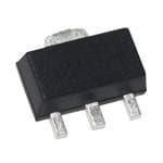
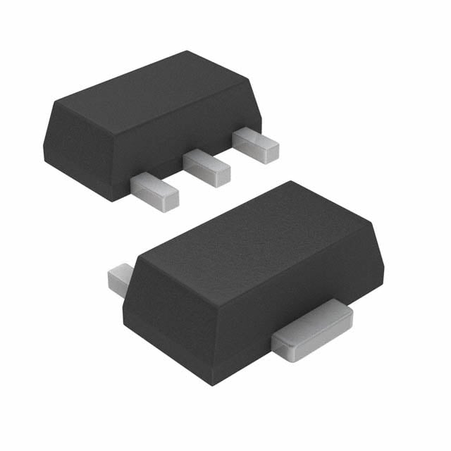
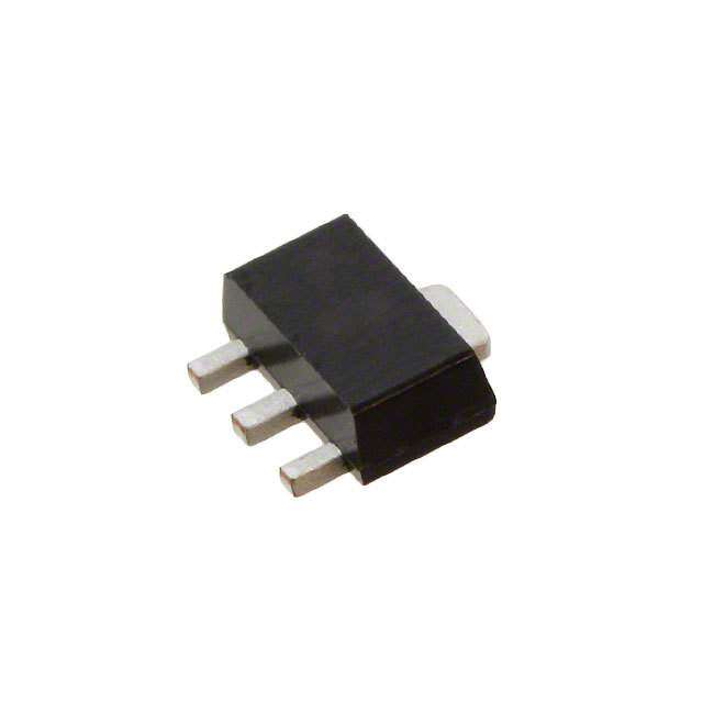
| 描述 | RF AMP 4GHZ 1/2 W SOT89射频放大器 Sot-89 1/2 W RF Driver Amplifier |
| 产品分类 | |
| 品牌 | Analog Devices |
| 产品手册 | |
| 产品图片 |
|
| rohs | 符合RoHS无铅 / 符合限制有害物质指令(RoHS)规范要求 |
| 产品系列 | RF集成电路,射频放大器,Analog Devices ADL5324ARKZ-R7- |
| 数据手册 | |
| P1dB | 28.5 dBm |
| 产品型号 | ADL5324ARKZ-R7 |
| RF类型 | ISM |
| 产品种类 | 射频放大器 |
| 供应商器件封装 | SOT-89-3 |
| 其它名称 | ADL5324ARKZ-R7DKR |
| 功率增益类型 | 12 dB |
| 包装 | Digi-Reel® |
| 商标 | Analog Devices |
| 噪声系数 | 4.4 dB |
| 增益 | 14.6dB |
| 安装风格 | SMD/SMT |
| 封装 | Reel |
| 封装/外壳 | TO-243AA |
| 封装/箱体 | SOT-89-3 |
| 工作电源电压 | 5 V |
| 工作频率 | 400 MHz to 4000 MHz |
| 工厂包装数量 | 1000 |
| 最大功率耗散 | 1.9 W |
| 最大工作温度 | + 105 C |
| 最小工作温度 | - 40 C |
| 标准包装 | 1 |
| 测试频率 | 3600 MHz |
| 特色产品 | http://www.digikey.com/product-highlights/cn/zh/analog-devices-adl5324-rf-driver-amplifier/1875 |
| 电压-电源 | 3.15 V ~ 5.25 V |
| 电流-电源 | 140mA |
| 电源电流 | 133 mA |
| 类型 | RF Driver |
| 系列 | ADL5324 |
| 视频文件 | http://www.digikey.cn/classic/video.aspx?PlayerID=1364138032001&width=640&height=505&videoID=2245193150001 |
| 输入返回损失 | - 10 dB |
| 输出截获点 | 36.6 dBm |
| 通道数量 | 1 Channel |
| 配用 | /product-detail/zh/ADL5324-EVALZ/ADL5324-EVALZ-ND/4866714 |
| 频率 | 400MHz ~ 4GHz |


- 商务部:美国ITC正式对集成电路等产品启动337调查
- 曝三星4nm工艺存在良率问题 高通将骁龙8 Gen1或转产台积电
- 太阳诱电将投资9.5亿元在常州建新厂生产MLCC 预计2023年完工
- 英特尔发布欧洲新工厂建设计划 深化IDM 2.0 战略
- 台积电先进制程称霸业界 有大客户加持明年业绩稳了
- 达到5530亿美元!SIA预计今年全球半导体销售额将创下新高
- 英特尔拟将自动驾驶子公司Mobileye上市 估值或超500亿美元
- 三星加码芯片和SET,合并消费电子和移动部门,撤换高东真等 CEO
- 三星电子宣布重大人事变动 还合并消费电子和移动部门
- 海关总署:前11个月进口集成电路产品价值2.52万亿元 增长14.8%


PDF Datasheet 数据手册内容提取
400 MHz to 4000 MHz ½ Watt RF Driver Amplifier Data Sheet ADL5324 FEATURES FUNCTIONAL BLOCK DIAGRAM Operation from 400 MHz to 4000 MHz GND Gain of 14.6 dB at 2140 MHz (2) OIP3 of 43.1 dBm at 2140 MHz ADL5324 P1dB of 29.1 dBm at 2140 MHz Noise figure of 3.8 dB BIAS DyAndajmusictaalblyle a pdojuwsetra bsulep bpilays b ias: 3.3 V to 5 V RF1IN GN2D RFO3UT 10562-001 Low power supply current: 62 mA to 133 mA Figure 1. No bias resistor needed Operating temperature range of −40°C to +105°C SOT-89 package, MSL-1 rated ESD rating of ±3 kV (Class 2) APPLICATIONS Wireless infrastructure Automated test equipment ISM/AMR applications GENERAL DESCRIPTION The ADL5324 incorporates a dynamically adjustable biasing The ADL5324 also delivers excellent ACPR vs. output power and circuit that allows for the customization of OIP3 and P1dB bias voltage. The driver can deliver greater than 17 dBm of output performance from 3.3 V to 5 V, without the need for an external power at 2140 MHz, while achieving an ACPR of −55 dBc at 5 V. If bias resistor. This feature gives the designer the ability to tailor the bias is reduced to 3.3 V, the −55 dBc ACPR output power driver amplifier performance to the specific needs of the design. only minimally reduces to 15 dBm. This feature also creates the opportunity for dynamic biasing of –30 the driver amplifier where a variable supply is used to allow for –35 full 5 V biasing under large signal conditions, and then reduced Bc) d–40 supply voltage when signal levels are smaller and lower power T ( SE–45 consumption is desirable. This scalability reduces the need to F F O–50 evaluate and inventory multiple driver amplifiers for different R output power requirements, from 25 dBm to 29 dBm output RIE–55 AR–60 SOURCE pTohwe eArD leLv5e3l2s.4 is also rated to operate across the wide temperature 5MHz C–65 VVCCCC==35.V3V @ –70 range of −40°C to +105°C for reliable performance in designs R P–75 that experience higher temperatures, such as power amplifiers. AC –80 The ½ W driver amplifier also covers the wide frequency range ocof m40p0o nMeHntzs ttoo b4e0 0tu0n MedH toz ,a a snpde coinfilcy b raenqdu wireitsh ain f ethwa te wxtiedren raaln ge. –85–20 –15 –10 –5 PO0UT (dB5m) 10 15 20 25 10562–055 This high performance broadband RF driver amplifier is well Figure 2. ACPR vs. Output Power, Single Carrier W-CDMA, suited for a variety of wired and wireless applications, including TM1-64 at 2140 MHz cellular infrastructure, ISM band power amplifiers, defense equipment, and instrumentation equipment. A fully populated evaluation board is available. Rev. B Information furnished by Analog Devices is believed to be accurate and reliable. However, no responsibility is assumed by Analog Devices for its use, nor for any infringements of patents or other One Technology Way, P.O. Box 9106, Norwood, MA 02062−9106, U.S.A. rights of third parties that may result from its use. Specifications subject to change without notice. No license is granted by implication or otherwise under any patent or patent rights of Analog Devices. Tel: 781.329.4700 www.analog.com Trademarks and registered trademarks are the property of their respective owners. Fax: 781.461.3113 ©2012 Analog Devices, Inc. All rights reserved.
ADL5324 Data Sheet TABLE OF CONTENTS Features .............................................................................................. 1 Typical Performance Characteristics ..............................................8 Applications ....................................................................................... 1 High Temperature Operation ................................................... 12 Functional Block Diagram .............................................................. 1 Applications Information .............................................................. 13 General Description ......................................................................... 1 Basic Layout Connections ......................................................... 13 Revision History ............................................................................... 2 Soldering Information and Recommended PCB Land Pattern. 13 Specifications ..................................................................................... 3 Matching Procedure ................................................................... 15 Typical Scattering Parameters ..................................................... 5 W-CDMA ACPR Performance ................................................ 16 Absolute Maximum Ratings ............................................................ 6 Evaluation Board ............................................................................ 17 Thermal Resistance ...................................................................... 6 Outline Dimensions ....................................................................... 20 ESD Caution .................................................................................. 6 Ordering Guide .......................................................................... 20 Pin Configuration and Function Descriptions ............................. 7 REVISION HISTORY 9/12—Rev. A to Rev. B 8/12—Rev. 0 to Rev. A Changes to Figure 27 ...................................................................... 11 Change 5 V Supply Current from 140 mA to 133 mA and 5 V Changed Figure 30 Tex t Reference to Figure 33 Text Reference ... 12 Power Dissipation from 700 mW to 665 mW, Table 1 ................. 4 Changed Table 7 Text Reference to Table 6 ................................. 15 Changes to Supply Current from 140 mA to 133 mA ............... 13 Changed Table 9 Text Reference to Table 10 and Table 10 Text 3/12—Revision 0: Initial Version Reference to Table 11 ..................................................................... 17 Changes to Figure 44 ...................................................................... 18 Rev. B | Page 2 of 20
Data Sheet ADL5324 SPECIFICATIONS VSUP = 5 V and T = 25°C, unless otherwise noted. A Table 1. 3.3 V 5 V Parameter Test Conditions/Comments Min Typ Max Min Typ Max Unit FREQUENCY = 457 MHz Gain 17.2 18.4 dB vs. Frequency ±37 MHz +0.0/−0.4 +0.0/−0.2 dB vs. Temperature −40°C ≤ T ≤ +85°C ±0.6 ±0.6 dB A vs. Supply 3.15 V to 3.45 V, 4.75 V to 5.25 V ±0.3 ±0.07 dB Output 1 dB Compression Point 24.2 28.0 dBm Output Third-Order Intercept ∆f = 1 MHz, P = 10 dBm per tone 30.1 40.1 dBm OUT Noise Figure 5.6 6.8 dB FREQUENCY = 748 MHz Gain 16.5 17.5 dB vs. Frequency ±20 MHz +0.0/−0.2 +0.0/−0.2 dB vs. Temperature −40°C ≤ T ≤ +85°C ±0.4 ±0.4 dB A vs. Supply 3.15 V to 3.45 V, 4.75 V to 5.25 V ±0.2 ±0.06 dB Output 1 dB Compression Point 24.2 28.0 dBm Output Third-Order Intercept ∆f = 1 MHz, P = 10 dBm per tone 36.0 45.8 dBm OUT Noise Figure 4.0 5.2 dB FREQUENCY = 915 MHz Gain1 15.8 16.0 16.8 17.6 dB vs. Frequency ±46 MHz ±0.1 +0.1/−0.3 dB vs. Temperature −40°C ≤ T ≤ +85°C ±0.4 ±0.4 dB A vs. Supply 3.15 V to 3.45 V, 4.75 V to 5.25 V ±0.2 ±0.06 dB Output 1 dB Compression Point 24.2 27.7 dBm Output Third-Order Intercept ∆f = 1 MHz, P = 10 dBm per tone 39.3 45.6 dBm OUT Noise Figure 4.1 5.1 dB FREQUENCY = 1935 MHz Gain 13.9 15.0 dB vs. Frequency ±55 MHz +0.0/−0.1 +0.0/−0.1 dB vs. Temperature −40°C ≤ T ≤ +85°C ±0.5 ±0.5 dB A vs. Supply 3.15 V to 3.45 V, 4.75 V to 5.25 V ±0.2 ±0.07 dB Output 1 dB Compression Point 23.2 27.2 dBm Output Third-Order Intercept ∆f = 1 MHz, P = 10 dBm per tone 34.6 45.5 dBm OUT Noise Figure 3.1 3.6 dB FREQUENCY = 2140 MHz Gain1 13.6 13.5 14.6 15.7 dB vs. Frequency ±30 MHz +0.1/−0.0 ±0.1 dB vs. Temperature −40°C ≤ T ≤ +85°C ±0.6 ±0.6 dB A vs. Supply 3.15 V to 3.45 V, 4.75 V to 5.25 V ±0.2 ±0.06 dB Output 1 dB Compression Point 25.3 29.1 dBm Output Third-Order Intercept ∆f = 1 MHz, P = 10 dBm per tone 34.4 43.1 dBm OUT Noise Figure 3.2 3.8 dB Rev. B | Page 3 of 20
ADL5324 Data Sheet 3.3 V 5 V Parameter Test Conditions/Comments Min Typ Max Min Typ Max Unit FREQUENCY = 2630 MHz Gain1 12.1 11.8 13.3 14.6 dB vs. Frequency ±60 MHz ±0.1 +0.0/−0.2 dB vs. Temperature −40°C ≤ T ≤ +85°C ±0.7 ±0.7 dB A vs. Supply 3.15 V to 3.45 V, 4.75 V to 5.25 V ±0.2 ±0.07 dB Output 1 dB Compression Point 23.6 27.8 dBm Output Third-Order Intercept ∆f = 1 MHz, P = 10 dBm per tone 32.4 42.0 dBm OUT Noise Figure 3.6 4.3 dB FREQUENCY = 3600 MHz Gain 11.0 12.0 dB vs. Frequency ±100 MHz +0.0/−0.7 +0.0/−0.8 dB vs. Temperature −40°C ≤ T ≤ +85°C ±1.0 ±1.0 dB A vs. Supply 3.15 V to 3.45 V, 4.75 V to 5.25 V ±0.2 ±0.05 dB Output 1 dB Compression Point 25.0 28.5 dBm Output Third-Order Intercept ∆f = 1 MHz, P = 10 dBm per tone 29.3 36.6 dBm OUT Noise Figure 3.8 4.4 dB POWER INTERFACE Pin RFOUT Supply Voltage 3.15 3.3 3.45 4.75 5 5.25 V Supply Current 62 133 mA vs. Temperature −40°C ≤ T ≤ +85°C +4/−6 +5/−7 mA A Power Dissipation VSUP = 5 V 205 665 mW 1 Guaranteed maximum and minimum specified limits on this parameter are based on six sigma calculations. Rev. B | Page 4 of 20
Data Sheet ADL5324 TYPICAL SCATTERING PARAMETERS VSUP = 5 V and T = 25°C; the effects of the test fixture have been de-embedded up to the pins of the device. A Table 2. S11 S21 S12 S22 Freq (MHz) Magnitude (dB) Angle (°) Magnitude (dB) Angle (°) Magnitude (dB) Angle (°) Magnitude (dB) Angle (°) 400 −0.73518 −178.582 13.3917 135.7023 −34.6804 12.40754 −3.04567 175.7277 500 −0.6682 178.6472 12.83594 125.9539 −34.2707 8.733014 −3.13245 175.9202 600 −0.69026 176.9348 12.14674 117.8626 −34.1019 6.416618 −3.13132 176.4634 700 −0.73622 175.8152 11.44082 111.0321 −34.0009 5.053048 −3.11375 177.3131 800 −0.78026 175.0847 10.7709 105.1552 −33.9042 3.90523 −3.08891 178.3368 900 −0.8238 174.5898 10.17296 99.91559 −33.7964 3.162531 −3.05337 179.4021 1000 −0.8703 174.2026 9.636511 95.21821 −33.6656 2.580227 −3.01719 −179.377 1100 −0.9211 173.9872 9.182607 91.01039 −33.5057 2.111382 −2.98741 −177.773 1200 −0.97114 173.3143 8.797653 86.68882 −33.3176 1.186726 −2.94972 −176.469 1300 −1.05332 172.9788 8.493785 82.89921 −33.0916 0.689198 −2.9749 −174.745 1400 −1.13807 172.418 8.268673 79.01047 −32.8261 −0.26086 −2.99624 −173.189 1500 −1.23342 171.5538 8.117951 74.96804 −32.5253 −1.43036 −3.02533 −171.783 1600 −1.34406 170.302 8.030017 70.69309 −32.1979 −3.08241 −3.04592 −170.675 1700 −1.47125 168.6736 7.998348 66.16438 −31.8306 −5.10232 −3.05748 −169.736 1800 −1.61396 166.5204 8.012977 61.23666 −31.4647 −7.75224 −3.08106 −169.23 1900 −1.78541 163.8113 8.0503 55.89288 −31.0967 −10.9203 −3.12034 −169.149 2000 −1.98158 160.6247 8.103461 50.12853 −30.7409 −14.671 −3.15588 −169.657 2100 −2.19535 157.0149 8.162658 43.95115 −30.4109 −19.0255 −3.18172 −170.862 2200 −2.43367 153.0489 8.207579 37.39437 −30.1134 −23.849 −3.19212 −172.621 2300 −2.68863 148.8413 8.231765 30.52801 −29.872 −29.1849 −3.17831 −174.879 2400 −2.95983 144.5491 8.231791 23.39294 −29.6822 −35.0026 −3.13204 −177.553 2500 −3.25472 140.354 8.199665 16.05117 −29.5353 −41.1796 −3.05541 179.4875 2600 −3.56594 136.4445 8.141897 8.510386 −29.4496 −47.7908 −2.94631 176.2481 2700 −3.90734 133.0736 8.052657 0.787456 −29.4307 −54.7743 −2.79325 172.8794 2800 −4.28173 130.4779 7.925075 −7.06584 −29.451 −62.1914 −2.57604 169.6831 2900 −4.69306 128.952 7.778394 −15.0835 −29.5362 −69.9289 −2.31023 166.7304 3000 −5.13012 128.7774 7.590076 −23.2924 −29.673 −78.1809 −2.00734 164.1571 3100 −5.54712 130.3019 7.355608 −31.6367 −29.8658 −86.8436 −1.69231 162.0214 3200 −5.86482 133.6487 7.062082 −40.2413 −30.1507 −96.2073 −1.37649 160.0906 3300 −5.98131 138.5443 6.680613 −48.9518 −30.5191 −106.08 −1.0663 158.4485 3400 −5.80159 144.0974 6.20792 −57.556 −30.9857 −116.217 −0.80053 157.172 3500 −5.34159 149.2672 5.63213 −65.9828 −31.5373 −126.686 −0.58238 156.1642 3600 −4.7127 153.2749 4.988874 −73.9355 −32.1461 −137.413 −0.41604 155.491 3700 −4.03208 155.8906 4.279792 −81.4065 −32.7942 −148.125 −0.30331 155.1641 3800 −3.37391 157.3335 3.543499 −88.1911 −33.4212 −158.775 −0.23714 155.0734 3900 −2.79798 157.8681 2.803935 −94.5028 −33.9833 −169.303 −0.20674 155.156 4000 −2.30194 157.7622 2.085365 −100.344 −34.3781 −179.983 −0.20598 155.3378 Rev. B | Page 5 of 20
ADL5324 Data Sheet ABSOLUTE MAXIMUM RATINGS THERMAL RESISTANCE Table 3. Table 4 lists the junction-to-air thermal resistance (θ ) and the Parameter Rating JA junction-to-paddle thermal resistance (θ ) for the ADL5324. Supply Voltage, VSUP 6.5 V JC Input Power (50 Ω Impedance) 20 dBm Table 4. Thermal Resistance Internal Power Dissipation (Paddle Soldered) 1.9 W Package Type θ 1 θ 2 Unit JA JC Maximum Junction Temperature 150°C 3-Lead SOT-89 37 9 °C/W Operating Temperature Range −40°C to +105°C Storage Temperature Range −65°C to +150°C 1Measured on Analog Devices evaluation board. For more information about board layout, see the Soldering Information and Recommended PCB Land Stresses above those listed under Absolute Maximum Ratings Pattern section. may cause permanent damage to the device. This is a stress 2Based on simulation with JEDEC standard JESD51. rating only; functional operation of the device at these or any other conditions above those indicated in the operational ESD CAUTION section of this specification is not implied. Exposure to absolute maximum rating conditions for extended periods may affect device reliability. Rev. B | Page 6 of 20
Data Sheet ADL5324 PIN CONFIGURATION AND FUNCTION DESCRIPTIONS RFIN 1 ADL5324 GND 2 TOP VIEW (2) GND (Not to Scale) RFOUT 3 10562-002 Figure 3. Pin Configuration Table 5. Pin Function Descriptions Pin No. Mnemonic Description 1 RFIN RF Input. This pin requires a dc blocking capacitor. 2 GND Ground. Connect this pin to a low impedance ground plane. Note that the paddle, which is exposed, encompasses Pin 2 and the tab at the top side of the package. It should be soldered to a low impedance ground plane for electrical grounding and thermal transfer. 3 RFOUT RF Output and Supply Voltage. DC bias is provided to this pin through an inductor that is connected to the external power supply. The RF path requires a dc blocking capacitor. Rev. B | Page 7 of 20
ADL5324 Data Sheet TYPICAL PERFORMANCE CHARACTERISTICS 50 35 50 Bm) 45 OIP3 (dBm) 34 48 d B, 40 33 +85°C 46 d 3 ( +25°C P 35 32 44 OI 1DB, 30 P1dB (dBm) Bm) 31 –40°C 42 Bm) N, P 25 B (d 30 40 3 (d E, GAI 20 GAIN (dB) P1d 29 +25°C 38 OIP UR 15 28 –40°C 36 G SE FI 10 NF (dB) 27 +85°C 34 OI 5 26 32 N 0869 884 900FREQUE9N15CY (MHz9)30 946 961 10562-015 25869 884 900FREQUE9N1C5Y (MHz9)30 946 96130 10562-018 Figure 4. Gain, P1dB, OIP3, and Noise Figure vs. Frequency, Figure 7. OIP3 and P1dB vs. Frequency and Temperature, 869 MHz to 961 MHz 869 MHz to 961 MHz 17.5 55 –40°C 53 51 17.0 +25°C 49 B) m) 47 d B AIN ( 16.5 +85°C P3 (d 45 G OI 43 41 16.0 39 869MHz 37 915MHz 961MHz 15.5869 884 900FREQUE9N1C5Y (MHz9)30 946 961 10562-016 35–5 0 POUT5 PER TONE 1(0dBm) 15 20 10562-019 Figure 5. Gain vs. Frequency and Temperature, 869 MHz to 961 MHz Figure 8. OIP3 vs. P and Frequency, 869 MHz to 961 MHz OUT 0 7 –5 S22 +85°C –10 6 ETERS (dB) ––2105 S11 GURE (dB) 5 +25°C M FI PARA –25 OISE –40°C S- S12 N –30 4 –35 –40869 884 900FREQUE9N1C5Y (MHz9)30 946 961 10562-017 3869 884 900FREQUE9N1C5Y (MHz9)30 946 961 10562-020 Figure 6. Input Return Loss (S11), Output Return Loss (S22), and Reverse Figure 9. Noise Figure vs. Frequency and Temperature, Isolation (S12) vs. Frequency, 869 MHz to 961 MHz 869 MHz to 961 MHz Rev. B | Page 8 of 20
Data Sheet ADL5324 50 35 48 Bm) 45 OIP3 (dBm) 34 46 d +25°C –40°C B, 40 33 44 d OIP3 ( 35 32 +85°C 42 1dB, 30 P1dB (dBm) Bm) 31 40 Bm) GAIN, P 2205 P1dB (d 2390 –40°C +25°C 3368 OIP3 (d E, GAIN (dB) UR 15 28 +85°C 34 G E FI 10 27 32 S NF (dB) OI 5 26 30 N 20110 2120 213F0REQUE21N4C0Y (MHz2)150 2160 2170 10562-027 225110 2120 213F0REQUE21N4C0Y (MHz2)150 2160 217208 10562-030 Figure 10. Gain, P1dB, OIP3, and Noise Figure vs. Frequency, Figure 13. OIP3 and P1dB vs. Frequency and Temperature, 2110 MHz to 2170 MHz 2110 MHz to 2170 MHz 16.0 50 2110MHz 48 2140MHz 15.5 2170MHz –40°C 46 44 15.0 B) +25°C m) 42 d B AIN ( 14.5 P3 (d 40 G OI 38 +85°C 14.0 36 34 13.5 32 13.20110 2120 213F0REQUE21N4C0Y (MHz2)150 2160 2170 10562-028 30–5 0 POUT5 PER TONE 1(0dBm) 15 20 10562-031 Figure 11. Gain vs. Frequency and Temperature, 2110 MHz to 2170 MHz Figure 14. OIP3 vs. P and Frequency, 2110 MHz to 2170 MHz OUT 0 6 –5 –10 S22 5 dB) B) +85°C RS ( –15 S11 E (d E R RAMET –20 S12 E FIGU 4 +25°C A –25 S P OI S- N –40°C –30 3 –35 –420110 2120 213F0REQUE21N4C0Y (MHz2)150 2160 2170 10562-029 22110 2120 213F0REQUE21N4C0Y (MHz2)150 2160 2170 10562-032 Figure 12. Input Return Loss (S11), Output Return Loss (S22), and Reverse Figure 15. Noise Figure vs. Frequency and Temperature, Isolation (S12) vs. Frequency, 2110 MHz to 2170 MHz 2110 MHz to 2170 MHz Rev. B | Page 9 of 20
ADL5324 Data Sheet 50 34 48 Bm) 45 OIP3 (dBm) 33 46 d B, 40 32 +25°C –40°C 44 d P3 ( 35 31 42 OI +85°C 1dB, 30 P1dB (dBm) Bm) 30 40 Bm) N, P 25 B (d 29 38 3 (d GAI 20 P1d 28 –40°C +25°C 36 OIP E, UR 15 GAIN (dB) 27 34 G +85°C E FI 10 26 32 OIS 5 NF (dB) 25 30 N 20570 2590 261F0REQUE26N3C0Y (MHz2)650 2670 2690 10562-033 224570 2590 261F0REQUE26N3C0Y (MHz2)650 2670 269208 10562-036 Figure 16. Gain, P1dB, OIP3, and Noise Figure vs. Frequency, Figure 19. OIP3 and P1dB vs. Frequency and Temperature, 2570 MHz to 2690 MHz 2570 MHz to 2690 MHz 14.5 50 2570MHz 48 2630MHz 14.0 –40°C 2690MHz 46 44 13.5 +25°C B) m) 42 d B AIN ( 13.0 P3 (d 40 G +85°C OI 38 12.5 36 34 12.0 32 11.25570 2590 261F0REQUE26N3C0Y (MHz2)650 2670 2690 10562-034 30–5 0 POUT5 PER TONE 1(0dBm) 15 20 10562-037 Figure 17. Gain vs. Frequency and Temperature, 2570 MHz to 2690 MHz Figure 20. OIP3 vs. P and Frequency, 2570 MHz to 2690 MHz OUT 0 7 –5 –10 S22 6 dB) B) RS ( –15 S11 E (d +85°C E R ET –20 GU 5 PARAM –25 S12 OISE FI +25°C S- N –30 4 –40°C –35 –420570 2590 261F0REQUE26N3C0Y (MHz2)650 2670 2690 10562-035 23570 2590 261F0REQUE26N3C0Y (MHz2)650 2670 2690 10562-038 Figure 18. Input Return Loss (S11), Output Return Loss (S22), and Reverse Figure 21. Noise Figure vs. Frequency and Temperature, Isolation (S12) vs. Frequency, 2570 MHz to 2690 MHz 2570 MHz to 2690 MHz Rev. B | Page 10 of 20
Data Sheet ADL5324 30 25 25 20 %) 20 %) E ( E ( 15 G G A A T 15 T N N E E RC RC 10 E E P 10 P 5 5 0 41.2 41.6 42.0 42.4 O42IP.83 (d4B3m.2) 43.6 44.0 44.4 44.8 10562-045 0 3.45 3.50 3.55 3.6N0OIS3E.6 F5IGU3.R70E (d3B.7)5 3.80 3.85 3.90 10562-048 Figure 22. OIP3 Distribution at 2140 MHz Figure 25. Noise Figure Distribution at 2140 MHz 50 200 45 190 40 180 E (%) 3305 NT (mA) 116700 AG RE 5.25V NT 25 UR 150 RCE 20 LY C 140 5V E P P 15 UP 130 4.75V S 10 120 5 110 0 28.2 28.4 28.6 28.8 P219d.0B (d2B9.m2) 29.4 29.6 29.8 30.0 10562-046 100–40 –20 0 TEMPE2R0ATURE 4(0°C) 60 80 10562-049 Figure 23. P1dB Distribution at 2140 MHz Figure 26. Supply Current vs. Supply Voltage and Temperature, 5 V (Using 2140 MHz Matching Components) 100 40 90 35 80 30 mA) 70 3.45V ENTAGE (%) 2205 Y CURRENT ( 456000 33..135VV C L PER 15 SUPP 30 10 20 5 10 0 14.3 14.4 14.5 14.6 1G4A.7IN (1d4B.8) 14.9 15.0 15.1 15.2 10562-047 0–40 –20 0 TEMPE2R0ATURE 4(0°C) 60 80 10562-064 Figure 24. Gain Distribution at 2140 MHz Figure 27. Supply Current vs. Supply Voltage and Temperature, 3.3 V (Using 2140 MHz Matching Components) Rev. B | Page 11 of 20
ADL5324 Data Sheet HIGH TEMPERATURE OPERATION The ADL5324 has excellent performance at temperatures above 85°C. At 105°C, the gain and P1dB decrease by 0.2 dB, the OIP3 decreases by 0.1 dB, and the noise figure increases by 0.31 dB compared with the data at 85°C. Figure 28 through Figure 33 show the performance at 105°C. 15.0 15.0 25°C 14.5 14.5 85°C 105°C 14.0 14.0 B) B) d d N ( 13.5 25°C N ( 13.5 AI 85°C AI G 105°C G 13.0 13.0 12.5 12.5 12.20110 2120 213F0REQUE21N4C0Y (MHz2)150 2160 2170 10562-134 12.20110 2120 213F0REQUE21N4C0Y (MHz2)150 2160 2170 10562-137 Figure 28. Gain vs. Frequency and Temperature, 5 V Supply, 2140 MHz Figure 31. Gain vs. Frequency and Temperature, 3.3 V Supply, 2140 MHz 33 48 33 48 OIP3 25°C 31 43 31 85°C 43 105°C m) 29 38 m) m) 29 38 m) B B B B B (d P1dB 3 (d B (d OIP3 3 (d d P d P P1 27 25°C 33 OI P1 27 33 OI 85°C 105°C 25 28 25 28 P1dB 232110 2120 213F0REQU2E1N4C0Y (MHz2)150 2160 217023 10562-135 232110 2120 213F0REQU2E1N4C0Y (MHz2)150 2160 217023 10562-138 Figure 29. OIP3 and P1dB vs. Frequency and Temperature, Figure 32. OIP3 and P1dB vs. Frequency and Temperature, 3.3 V Supply, 5 V Supply, 2140 MHz 2140 MHz 6 6 25°C 25°C 85°C 85°C 105°C 105°C 5 5 B) B) E (d E (d R R U U FIG4 FIG4 E E S S OI OI N N 3 3 22110 2120 213F0REQUE21N4C0Y (MHz2)150 2160 2170 10562-136 22110 2120 213F0REQUE21N4C0Y (MHz2)150 2160 2170 10562-139 Figure 30. Noise Figure vs. Frequency and Temperature, 5 V Supply, Figure 33. Noise Figure vs. Frequency and Temperature, 3.3 V Supply, 2140 MHz 2140 MHz Rev. B | Page 12 of 20
Data Sheet ADL5324 APPLICATIONS INFORMATION BASIC LAYOUT CONNECTIONS SOLDERING INFORMATION AND RECOMMENDED PCB LAND PATTERN The basic connections for operating the ADL5324 are shown in Figure 34. Table 6 lists the required matching components. Figure 35 shows the recommended land pattern for the ADL5324. Capacitors C1, C2, and C3 are Murata GRM615 series (0402 To minimize thermal impedance, the exposed paddle on the size) High Q capacitors and C7 is a Murata GRM155 series SOT-89 package underside is soldered to a ground plane along (0402 size). Inductor L1 is a Coilcraft 0603CS series (0603 size). with Pin 2. If multiple ground layers exist, they should be For all frequency bands, the placement of C1 and C2 are critical. stitched together using vias. For more information on land The placement of C3 becomes critical for the following bands: pattern design and layout, refer to the Application Note AN-772, 1880 MHz to 1990 MHz, 2110 MHz to 2170 MHz, 2300 MHz to A Design and Manufacturing Guide for the Lead Frame Chip 2400 MHz, 2570 MHz to 2690 MHz. and 3500 MHz to 3600 MHz. Scale Package (LFCSP). For operation from 420 MHz to 494 MHz, 728 MHz to 768 MHz, This land pattern, on the ADL5324 evaluation board, provides and 869 MHz to 960 MHz, R2 is replaced with a Coilcraft (0402 a measured thermal resistance (θ ) of 37°C/W. To measure θ , JA JA size) High Q inductor. Table 7 lists the recommended component the temperature at the top of the SOT-89 package is found with placement for various frequencies. an IR temperature gun. Thermal simulation suggests a junction A 5 V dc bias is supplied through L1, which is connected to temperature 10°C higher than the top of package temperature. RFOUT (Pin 3). In addition to C4, 10 nF and 10 µF power supply With additional ambient temperature and I/O power decoupling capacitors are also required. The typical current measurements, θJA could be determined. consumption for the ADL5324 is 133 mA. 1.80mm GND VSUP C6 10µF D N C5 10nF (2) G 3.48mm C4 100pF ADL5324 0.20mm L1 5.56mm RFIN0RΩ1 2C.43p3F λ12 RFIN1 GND2 OUT3 15λn2H2 0RΩ2 2C0p7F RFOUT F R C13 C23 2pF 2.2pF 0.86mm 0.62mm 1SEE THE RECOMMENDED COMPONENTS FOR BASIC CONNECTIONSTABLE 23SCFOE1,ER C TF2AR,BAELNQEDU 6EC NF3COAYRR- SERP EMECUCORIFMAIMCTA EC NHODIMGEHPDO QCN OCEMANPTPASOC.NIETONTR SS PGARCMIN61G5. SERIES. 10562-050 1.27mm Figure 34. Basic Connections 1.50mm3.00mm 10562-051 Figure 35. Recommended Land Pattern Rev. B | Page 13 of 20
ADL5324 Data Sheet Table 6. Recommended Components for Basic Connections 2110 MHz to Function/ 420 MHz to 728 MHz to 800 MHz to 1880 MHz to 2170 MHz 2300 MHz to 2560 MHz to 3500 MHz to Component 494 MHz 768 MHz 960 MHz 1990 MHz (Default) 2400 MHz 2690 MHz 3700 MHz AC Coupling Capacitors C3 = 0402 10 pF 10pF1 10 pF1 2.4 pF1 2.4 pF1 2.4 pF1 2pF1 1pF1 C7 = 0402 20 pF 20 pF 20 pF 20 pF 20 pF 20 pF 20 pF1 20 pF Power Supply Bypassing Capacitors C4 = 0402 100 pF 100 pF 100 pF 100 pF 100 pF 100 pF 100 pF 100 pF C5 = 0603 10 nF 10 nF 10 nF 10 nF 10 nF 10 nF 10 nF 10 nF C6 = 1206 10 µF 10 µF 10 µF 10 µF 10 µF 10 µF 10 µF 10 µF DC Bias Inductor 120 nH 18 nH 18 nH 15 nH 15 nH 15 nH 15 nH 15 nH L1 = 0603CS Tuning Capacitors C1 = 0402 20 pF1 8 pF1 8 pF1 2.4 pF1 2.0 pF1 1.5 pF1 1.0 pF1 0.5 pF1 C2 = 0402 6.2 pF1 3.9 pF1 3.6 pF1 2.4 pF1 2.2 pF1 2.0 pF1 2.0 pF1 0.75 pF1 Jumpers R1 = 0402 2 Ω 2 Ω 2 Ω 0 Ω 0 Ω 0 Ω 0 Ω 0 Ω R2 = 0402 5.6 nH2 2.4 nH3 2.4 nH3 0 Ω 0 Ω 0 Ω 0 Ω 4.7 nH3 Power Supply Connections VSUP Red test loop GND Black test loop 1 Murata High Q capacitor. 2 Add a 1.6 nH at input (see Figure 41). 3 Coilcraft 0402CS series. Table 7. Matching Component Spacing Frequency (MHz) λ1 (mils) λ2 (mils) 420 to 494 419 438 728 to 768 311 422 869 to 961 207 413 1880 to 1990 75 239 2110 to 2170 65 193 2300 to 2400 71 176 2570 to 2690 245 132 3500 to 3700 316 125 Rev. B | Page 14 of 20
Data Sheet ADL5324 MATCHING PROCEDURE 4. Repeat Step 3 as necessary. Once the desired gain and return loss are realized, measure OIP3. Most likely, it will be The ADL5324 is designed to achieve excellent gain and OIP3 necessary to go back and forth between return loss/gain and performance. To achieve this, both input and output matching OIP3 measurements (probably compromising most on output networks must present specific impedance to the device. The return loss) until an acceptable compromise is achieved. matching components listed in Table 6 were chosen to provide −10 dB input return loss while maximizing OIP3. Fixed Load Pull Freq = 2.1400 GHz ZSource_2nd (Ohms) : 50.00 + j 0.00 The load-pull plots (see Figure 36 and Figure 37) show the load ZSource_3rd (Ohms) : 50.00 + j 0.00 Load Gt max = 16.06 dB impedance points on the Smith chart where optimum OIP3, gain, at 2.97 – j2.70 Ohms 10 contours, 0.50 dB step and output power can be achieved. These load impedance values (11.50 to 16.00 dB) Ip3 max = 44.18 dBm (that is, the impedance that the device sees when looking into 10 acto n t 9o.u4r4s ,+ j91..6050 OdBhmm sstep (35.00 to 44.00 dBm) the output matching network) are listed in Table 8 and Table 9 Specs: OFF for maximum gain and maximum OIP3, respectively. The contours show how each parameter degrades as it is moved away from the optimum point. From the data shown in Table 8 and Table 9, it becomes clear that maximum gain and maximum OIP3 do not occur at the same impedance. This can also be seen on the load-pull contours in Figure 36 and Figure 37. Thus, output matching generally involves compromising between gain and OIP3. In addition, the load- LAaDbLe5l3:24_2P14_LP7 10562-053 pull plots demonstrate that the quality of the output impedance Figure 36. Load-Pull Contours, 2140 MHz match must be compromised to optimize gain and/or OIP3. In Fixed Load Pull most applications where line lengths are short and where the Freq = 2.6300 GHz next device in the signal chain presents a low input return loss, ZZSSoouurrccee _(2Onhdms(O) :h 4m9s.8) 4: 3+7 j. 749.3 +3 j 3.28 Load ZSource_3rd (Ohms) : 39.74 + j10.00 compromising on the output match is acceptable. Gt max = 13.83 dB at 4.27 – j1.99 Ohms 10 contours, 0.50 dB step To adjust the output match for operation at a different frequency, (9.00 to 13.50 dB) Ip3 max = 45.19 dBm or if a different trade-off between OIP3, gain, and output at 2.84 + j5.89 Ohms 10 contours, 1.00 dBm step (36.00 to 45.00 dBm) impedance is desired, a four-step procedure is recommended. Specs: OFF For example, to optimize the ADL5324 for optimum OIP3 and gain at 750 MHz, use the following steps: 1. Install the recommended tuning components for an 869 MHz to 970 MHz tuning band, but do not install C1 and C2. 2. Connect the evaluation board to a vector network analyzer ssiom thualtta innepouuts alyn. d output return loss can be viewed 26.37 + j30.90 LAaDbLe5l3:24_2p63ghZ_LP3 10562-054 3. Starting with the recommended values and positions for Figure 37. Load-Pull Contours, 2600 MHz C1 and C2, adjust the positions of these capacitors along the Table 8. Load Conditions for Gain transmission line until the return loss and gain are acceptable. MAX ΓLoad In this case, push-down capacitors mounted on small sticks Frequency (MHz) (Magnitude) ΓLoad (°) Gain (dB) can be used as an alternative to soldering. If moving the MAX 2140 0.888 −173.55 16.1 component positions does not yield satisfactory results, 2630 0.0843 −175.41 13.83 then increase or decrease the values of C1 and C2 (in this case, the values are most likely increased because the user Table 9. Load Conditions for OIP3 is tuning for a lower frequency. MAX ΓLoad Frequency (MHz) (Magnitude) ΓLoad (°) IP3 (dBm) MAX 2140 0.654 +163.28 44.18 2630 0.894 +166.52 45.19 Rev. B | Page 15 of 20
ADL5324 Data Sheet W-CDMA ACPR PERFORMANCE –30 –35 Figure 38 shows a plot of adjacent channel power ratio (ACPR) vs. c) B d–40 cPaOrUrTi eforr ( tThees tA MDoLd53el2 14-. 6T4h)e a sti g2n1a4l0 t yMpeH uzs.e Tdh isis a s siignngalel iWs g-CenDeMratAe d SET (–45 F F by a very low ACPR source. ACPR is measured at the output by O–50 R a high dynamic range spectrum analyzer, which incorporates an RIE–55 instrument noise correction function. AR–60 SOURCE The ADL5324 achieves an ACPR of −79 dBc at 0 dBm output, MHz C–65 VVCCCC==35.V3V 5 at which point device noise and not distortion is beginning to @ –70 R dominate the power in the adjacent channels. At an output power CP–75 A of 10 dBm, ACPR is still very low at −72 dBc, making the device –80 particularly suitable for PA driver applications. –85–20 –15 –10 –5 PO0UT (dB5m) 10 15 20 25 10562–155 Figure 38. ACPR vs. Output Power, Single Carrier W-CDMA, TM1-64, at 2140 MHz Rev. B | Page 16 of 20
Data Sheet ADL5324 EVALUATION BOARD The schematic of the ADL5324 evaluation board is shown in Figure 39. This evaluation board uses 25 mil wide traces and is made from FR4 material. The evaluation board comes tuned for operation in the 2110 MHz to 2170 MHz tuning band. Tuning options for other frequency bands are also provided in Table 10. The recommended placement for these components is provided in Table 11. The inputs and outputs should be ac-coupled with 100pF C3 L1 R2 appropriately sized capacitors. dc bias is provided to the amplifier 2.4pF 15nH 0Ω via an inductor connected to the RFOUT pin. A bias voltage of R1 C7 0Ω C2 20pF 5 V is recommended. 193mils 2.2pF 65mils C1 GND VSUP 2pF C6 10µF D N C5 10nF (2) G C4 100pF RFIN 0RΩ12C.43p1F λ14 RFIN1ADGNDL2532OUT43 L151nλH24 0RΩ2 2C0p7F RFOUT Figure 40. Evaluation Board Layout and Default Component Placement fo10562-057r F 2110 MHz to 2170 MHz R C12 C23 2pF 2.2pF 1MURATA HIGH Q CAPACITOR GRM615COG2R4B50 OR EQUIVALENT. 234MMSEUUERR AATATTAAB LHHEIIGG 1HH0 FQQO CCRAA RPPEAACCCOIITTMOOMRRE GGNRRDMME66D11 C55CCOOOMGGP02O2RN02EBBN550T0 OOSRPR A EECQQINUUGIIVV.AALLEENNTT.. 10562-056 Figure 39. Evaluation Board, 2110 MHz to 2170 MHz Table 10. Recommended Components for Basic Connections 2110 MHz to Function/ 420 MHz to 728 MHz to 800 MHz to 1880 MHz to 2170 MHz 2300 MHz to 2560 MHz to 3500 MHz to Component 494 MHz 768 MHz 960 MHz 1990 MHz (Default) 2400 MHz 2690 MHz 3700 MHz AC Coupling Capacitors C3 = 0402 10 pF 10pF1 10 pF 2.4 pF1 2.4 pF1 2.4 pF1 2pF1 1pF1 C7 = 0402 20 pF 20 pF 20 pF 20 pF 20 pF 20 pF 20 pF1 20 pF Power Supply Bypassing Capacitors C4 = 0402 100 pF 100 pF 100 pF 100 pF 100 pF 100 pF 100 pF 100 pF C5 = 0603 10 nF 10 nF 10 nF 10 nF 10 nF 10 nF 10 nF 10 nF C6 = 1206 10 µF 10 µF 10 µF 10 µF 10 µF 10 µF 10 µF 10 µF DC Bias Inductor 120 nH 18 nH 18 nH 15 nH 15 nH 15 nH 15 nH 15 nH L1 = 0603CS Tuning Capacitors C1 = 0402 20 pF1 8 pF1 8 pF1 2.4 pF1 2.0 pF1 1.5 pF1 1.0 pF1 0.5 pF1 C2 = 0402 6.2 pF1 3.9 pF1 3.6 pF1 2.4 pF1 2.2 pF1 2.0 pF1 2.0 pF1 0.75 pF1 Jumpers R1 = 0402 2 Ω 2 Ω 2 Ω 0 Ω 0 Ω 0 Ω 0 Ω 0 Ω R2 = 0402 5.6 nH2 2.4 nH3 2.4 nH3 0 Ω 0 Ω 0 Ω 0 Ω 4.7 nH3 Power Supply Connections VSUP Red test loop GND Black test loop 1 Murata High Q capacitor. 2 Add a 1.6 nH at input (see Figure 41). 3 Coilcraft 0402CS series. Rev. B | Page 17 of 20
ADL5324 Data Sheet Table 11. Recommended Component Spacing on Evaluation Board Frequency (MHz) λ1 (mils) λ2 (mils) 420 to 494 419 438 728 to 768 311 422 869 to 961 207 413 1880 to 1990 75 239 2110 to 2170 65 193 2300 to 2400 71 176 2570 to 2690 245 132 3500 to 3700 316 125 100 pF 100pF 2C0p1F 1.L6n3H 2RΩ1 L1210nH L5.26nH 2C0p7F L1 L2.24nH 18nH C3 248 mils 311 mils C2 C3 C1 R1 C7 10pF 419 mils 438 mils 6.2pF 10pF 8pF 2Ω 413mils C2 20pF 207mils 3.6pF 10562-042 10562-060 Figure 41. Evaluation Board Layout and Component Placement, Figure 43. Evaluation Board Layout and Component Placement, 420 MHz to 494 MHz Operation 869 MHz to 961 MHz Operation 100pF 100pF 8Cp1F 2RΩ1 L181nH 2.L4n2H 2C0p7F C2.34pF L151nH 0RΩ2 C3 R1 C7 10pF 311 mils 422 mils C3.29pF 0Ω 75mils 239mils C2.24pF 20pF C1 2.4pF 10562-043 10562-061 Figure 42. Evaluation Board Layout and Component Placement, Figure 44. Evaluation Board Layout and Component Placement, 728 MHz to 768 MHz Operation 1880 MHz to 1990 MHz Operation Rev. B | Page 18 of 20
Data Sheet ADL5324 100pF 100pF C2.34pF L151nH 0RΩ2 0.C51pF 1.C03pF L151nH 4.L7n2H 2C0p7F 0RΩ1 C2 C207pF 0RΩ1 316 mils C0.275pF 176mils 2.0pF 125 mils 71mils C1 1.5pF 10562-062 10562-148 Figure 45. Evaluation Board Layout and Component Placement, Figure 47. Evaluation Board Layout and Component Placement, 2300 MHz to 2400 MHz Operation 3500 MHz to 3700 MHz Operation 100pF C3 L1 C7 2.0pF 15nH 20pF R1 R2 0Ω C1 C2 0Ω 1.0pF 245mils 132mils 2.0pF 10562-063 Figure 46. Evaluation Board Layout and Component Placement, 2560 MHz to 2690 MHz Operation Rev. B | Page 19 of 20
ADL5324 Data Sheet OUTLINE DIMENSIONS *1.75 1.55 4.25 (2) 2.60 3.94 2.30 1 2 3 1.20 1.50TYP 0.75 3.00TYP 2.29 4.60 2.14 4.40 1.60 1.40 0.44 0.35 *0.56 ENDVIEW 0.36 *0.52 0.32 *ECXOCMEPPLTIAIONNTOTFODJIEMDEENCSSIOTNASNDINADRICDASTTEOD-2B4Y3AWNITAHSTTHEERISK. 12-18-2008-B Figure 48. 3-Lead Small Outline Transistor Package [SOT-89] (RK-3) Dimensions shown in millimeters ORDERING GUIDE Model1 Temperature Range Package Description Package Option ADL5324ARKZ-R7 −40°C to +105°C 3-Lead SOT-89, 7“ Tape and Reel RK-3 ADL5324-EVALZ Evaluation Board 1 Z = RoHS Compliant Part. ©2012 Analog Devices, Inc. All rights reserved. Trademarks and registered trademarks are the property of their respective owners. D10562-0-9/12(B) Rev. B | Page 20 of 20
Mouser Electronics Authorized Distributor Click to View Pricing, Inventory, Delivery & Lifecycle Information: A nalog Devices Inc.: ADL5324ARKZ-R7 ADL5324-EVALZ