ICGOO在线商城 > 射频/IF 和 RFID > RF 放大器 > ADL5240ACPZ-R7
- 型号: ADL5240ACPZ-R7
- 制造商: Analog
- 库位|库存: xxxx|xxxx
- 要求:
| 数量阶梯 | 香港交货 | 国内含税 |
| +xxxx | $xxxx | ¥xxxx |
查看当月历史价格
查看今年历史价格
ADL5240ACPZ-R7产品简介:
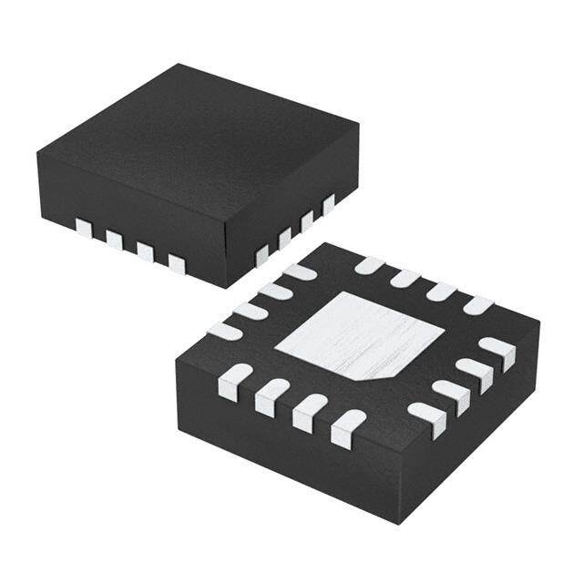
ICGOO电子元器件商城为您提供ADL5240ACPZ-R7由Analog设计生产,在icgoo商城现货销售,并且可以通过原厂、代理商等渠道进行代购。 ADL5240ACPZ-R7价格参考。AnalogADL5240ACPZ-R7封装/规格:RF 放大器, 射频放大器 IC 100MHz ~ 4GHz 32-LFCSP-VQ(5x5)。您可以下载ADL5240ACPZ-R7参考资料、Datasheet数据手册功能说明书,资料中有ADL5240ACPZ-R7 详细功能的应用电路图电压和使用方法及教程。
ADL5240ACPZ-R7 是 Analog Devices Inc. 生产的一款 RF(射频)放大器,具体型号为 ADL5240。其应用场景主要集中在射频信号的处理和放大领域,适用于多种通信、测试测量及无线设备系统中。以下是其主要应用场景:

1. 无线通信基础设施
   - 用于基站、中继器和其他无线通信设备中的射频信号放大。
   - 支持 GSM、CDMA、WCDMA 和 LTE 等多种通信标准,提供高线性度和低失真的性能。

2. 测试与测量设备
   - 在信号发生器、频谱分析仪等测试设备中用作驱动放大器或缓冲放大器。
   - 提供稳定的增益和宽频率范围,确保测试结果的准确性。

3. 雷达系统
   - 应用于脉冲雷达或连续波雷达系统中的信号放大。
   - 其宽带特性能够满足不同雷达频段的需求,同时保持低噪声和高动态范围。

4. 医疗设备
   - 在超声波设备或其他需要高频信号放大的医疗应用中使用。
   - 提供精确的信号放大能力,支持高质量图像生成。

5. 卫星通信
   - 用于地面站或用户终端中的射频信号放大,确保信号传输的质量和稳定性。
   - 适应 Ku 波段、C 波段等常见卫星通信频段。

6. 物联网 (IoT) 和短距离无线通信
   - 在 Zigbee、蓝牙、Wi-Fi 等短距离无线通信模块中,作为功率放大器或前置放大器。
   - 提高信号覆盖范围和传输效率。

7. 航空航天与国防
   - 在导航、通信和电子战系统中,用于射频信号的放大和处理。
   - 满足严苛环境下的高性能要求。

ADL5240ACPZ-R7 的关键特性包括:工作频率范围为 50 MHz 至 2.5 GHz,增益约为 20 dB,低噪声系数以及出色的线性度。这些特点使其成为上述应用场景的理想选择。
| 参数 | 数值 |
| 产品目录 | |
| 描述 | IC RF FILTER VGA 32-LFCSP射频放大器 100 MHz to 4000 MHz Digitally Cont VGA |
| 产品分类 | |
| 品牌 | Analog Devices Inc |
| 产品手册 | |
| 产品图片 |
|
| rohs | 符合RoHS无铅 / 符合限制有害物质指令(RoHS)规范要求 |
| 产品系列 | RF集成电路,射频放大器,Analog Devices ADL5240ACPZ-R7- |
| 数据手册 | |
| P1dB | 18.8dB |
| 产品型号 | ADL5240ACPZ-R7 |
| PCN组件/产地 | |
| RF类型 | - |
| 产品种类 | 射频放大器 |
| 供应商器件封装 | 32-LFCSP-VQ(5x5) |
| 其它名称 | ADL5240ACPZ-R7CT |
| 功率增益类型 | 19.7 dB |
| 包装 | 剪切带 (CT) |
| 商标 | Analog Devices |
| 噪声系数 | 3.1dB |
| 增益 | 19.6dB |
| 封装 | Reel |
| 封装/外壳 | 32-VFQFN 裸露焊盘,CSP |
| 封装/箱体 | LFCSP EP |
| 工作电源电压 | 5.25 V |
| 工作频率 | 4000 MHz |
| 工厂包装数量 | 1500 |
| 最大工作温度 | + 85 C |
| 最小工作温度 | - 40 C |
| 标准包装 | 1 |
| 测试频率 | 3.6GHz |
| 特色产品 | http://www.digikey.com/product-highlights/cn/zh/analog-devices-adl-rf-ics/1397 |
| 电压-电源 | 4.75 V ~ 5.25 V |
| 电流-电源 | 93mA |
| 电源电流 | 93 mA |
| 类型 | Digital Variable Gain Amplifier |
| 系列 | ADL5240 |
| 视频文件 | http://www.digikey.cn/classic/video.aspx?PlayerID=1364138032001&width=640&height=505&videoID=2245193150001 |
| 输入返回损失 | 10 dB at 2700 MHz |
| 输出截获点 | 41 dBm |
| 通道数量 | 1 Channel |
| 配用 | /product-detail/zh/ADL5240-EVALZ/ADL5240-EVALZ-ND/4866713 |
| 频率 | 100MHz ~ 4GHz |




- 商务部:美国ITC正式对集成电路等产品启动337调查
- 曝三星4nm工艺存在良率问题 高通将骁龙8 Gen1或转产台积电
- 太阳诱电将投资9.5亿元在常州建新厂生产MLCC 预计2023年完工
- 英特尔发布欧洲新工厂建设计划 深化IDM 2.0 战略
- 台积电先进制程称霸业界 有大客户加持明年业绩稳了
- 达到5530亿美元!SIA预计今年全球半导体销售额将创下新高
- 英特尔拟将自动驾驶子公司Mobileye上市 估值或超500亿美元
- 三星加码芯片和SET,合并消费电子和移动部门,撤换高东真等 CEO
- 三星电子宣布重大人事变动 还合并消费电子和移动部门
- 海关总署:前11个月进口集成电路产品价值2.52万亿元 增长14.8%





PDF Datasheet 数据手册内容提取
100 MHz to 4000 MHz RF/IF Digitally Controlled VGA Data Sheet ADL5240 FEATURES GENERAL DESCRIPTION Operating frequency from 100 MHz to 4000 MHz The ADL5240 is a high performance, digitally controlled variable Digitally controlled VGA with serial and parallel interfaces gain amplifier (VGA) operating from 100 MHz to 4000 MHz. 6-bit, 0.5 dB digital step attenuator The VGA integrates a high performance, 20 dB gain, internally 31.5 dB gain control range with ±0.25 dB step accuracy matched amplifier (AMP) with a 6-bit digital step attenuator Gain block amplifier specifications (DSA) that has a gain control range of 31.5 dB in 0.5 dB steps Gain: 19.7 dB at 2.14 GHz with ±0.25 dB step accuracy. The attenuation of the DSA can be OIP3: 41.0 dBm at 2.14 GHz controlled using a serial or parallel interface. P1dB: 19.5 dBm at 2.14 GHz Both the gain block and DSA are internally matched to 50 Ω at Noise figure: 2.9 dB at 2.14 GHz their inputs and outputs and are separately biased. The separate Gain block or digital step attenuator can be first bias allows all or part of the ADL5240 to be used, which facilitates Single supply operation from 4.75 V to 5.25 V easy reuse throughout a design. The pinout of the ADL5240 also Low quiescent current of 93 mA enables either the gain block or DSA to be first, giving the VGA Thermally efficient, 5 mm × 5 mm, 32-lead LFCSP maximum flexibility in a signal chain. The companion ADL5243 integrates a ¼ W driver amplifier to the output of the gain block and DSA The ADL5240 consumes just 93 mA and operates from a single supply ranging from 4.75 V to 5.25 V. The VGA is packaged in a APPLICATIONS thermally efficient, 5 mm × 5 mm, 32-lead LFCSP and is fully Wireless infrastructure specified for operation from −40°C to +85°C. A fully populated Automated test equipment evaluation board is available. RF/IF gain control FUNCTIONAL BLOCK DIAGRAM A K T L A E EL 0/C 1/D 2/L 3 4 5 6 S D D D D D D D 32 31 30 29 28 27 26 25 VDD 1 24 VDD SERIAL/PARALLEL INTERFACE NC 2 23 NC NC 3 22 NC DSAIN 4 21 DSAOUT 0.5dB 1dB 2dB 4dB 8dB 16dB NC 5 20 NC NC 6 19 NC ADL5240 NC 7 AMP 18 NC NC 8 17 NC 9 10 11 12 13 14 15 16 C C C C C C N C N AMPOUT/VC N N N N AMPI N 09430-001 Figure 1. Rev. A Document Feedback Information furnished by Analog Devices is believed to be accurate and reliable. However, no responsibility is assumed by Analog Devices for its use, nor for any infringements of patents or other rights of third parties that may result from its use. Specifications subject to change without notice. No One Technology Way, P.O. Box 9106, Norwood, MA 02062-9106, U.S.A. license is granted by implication or otherwise under any patent or patent rights of Analog Devices. Tel: 781.329.4700 ©2011–2013 Analog Devices, Inc. All rights reserved. Trademarks and registered trademarks are the property of their respective owners. Technical Support www.analog.com
ADL5240 Data Sheet TABLE OF CONTENTS Features .............................................................................................. 1 Applications Information .............................................................. 16 Applications ....................................................................................... 1 Basic Layout Connections ......................................................... 16 General Description ......................................................................... 1 SPI Timing................................................................................... 18 Functional Block Diagram .............................................................. 1 Loop Performance ...................................................................... 20 Revision History ............................................................................... 2 Amplifier Drive Level for Optimum ACLR ............................ 22 Specifications ..................................................................................... 3 Thermal Considerations ............................................................ 22 Absolute Maximum Ratings ............................................................ 8 Evaluation Board ............................................................................ 23 ESD Caution .................................................................................. 8 Outline Dimensions ....................................................................... 28 Pin Configuration and Function Descriptions ............................. 9 Ordering Guide .......................................................................... 28 Typical Performance Characteristics ........................................... 10 REVISION HISTORY 6/13—Rev. 0 to Rev. A Changes to Table 1 ............................................................................. 4 Changes to Table 3 ............................................................................. 9 Changes to Figure 3 ......................................................................... 11 Changes to Figure 16 ....................................................................... 12 Added Figure 29, Renumbered Sequentially ............................... 14 Changes to Table 5, Figure 35, and Figure 36 .............................. 18 Added Amplifier Drive Level for Optimum ACLR Section and Figure 39 .................................................................................... 22 Changes to Evaluation Board Section ........................................... 23 Changes to Figure 41 and Table 8 .................................................. 24 Added Figure 42 ............................................................................... 25 Changes to Figure 43 and Figure 44 .............................................. 26 Added Figure 45 ............................................................................... 27 7/11—Revision 0: Initial Version Rev. A | Page 2 of 28
Data Sheet ADL5240 SPECIFICATIONS VDD = 5 V, VCC = 5 V, T = 25oC A Table 1. Parameter Test Conditions/Comments Min Typ Max Unit OVERALL FUNCTION Frequency Range 100 4000 MHz AMPLIFIER FREQUENCY = 150 MHz Using the AMPIN and AMPOUT pins Gain 17.6 dB vs. Frequency ±50 MHz ±1.0 dB vs. Temperature −40°C ≤ T ≤ +85°C ±0.04 dB A vs. Supply 4.75 V to 5.25 V ±0.04 dB Input Return Loss S11 −10.4 dB Output Return Loss S22 −7.7 dB Output 1 dB Compression Point 18.3 dBm Output Third-Order Intercept ∆f = 1 MHz, P = 4 dBm/tone 30.0 dBm OUT Noise Figure 2.8 dB AMPLIFIER FREQUENCY = 450 MHz Using the AMPIN and AMPOUT pins Gain 20.3 dB vs. Frequency ±50 MHz ±0.11 dB vs. Temperature −40°C ≤ T ≤ +85°C ±0.36 dB A vs. Supply 4.75 V to 5.25 V ±0.01 dB Input Return Loss S11 −18.3 dB Output Return Loss S22 −15.7 dB Output 1 dB Compression Point 20.2 dBm Output Third-Order Intercept ∆f = 1 MHz, P = 4 dBm/tone 39.0 dBm OUT Noise Figure 2.9 dB AMPLIFIER FREQUENCY = 748 MHz Using the AMPIN and AMPOUT pins Gain 20.6 dB vs. Frequency ±50 MHz ±0.01 dB vs. Temperature −40°C ≤ T ≤ +85°C ±0.31 dB A vs. Supply 4.75 V to 5.25 V ±0.01 dB Input Return Loss S11 −25.7 dB Output Return Loss S22 −23.7 dB Output 1 dB Compression Point 20.2 dBm Output Third-Order Intercept ∆f = 1 MHz, P = 4 dBm/tone 40.0 dBm OUT Noise Figure 2.7 dB AMPLIFIER FREQUENCY = 943 MHz Using the AMPIN and AMPOUT pins Gain 19.0 20.5 22.0 dB vs. Frequency ±18 MHz ±0.01 dB vs. Temperature −40°C ≤ T ≤ +85°C ±0.27 dB A vs. Supply 4.75 V to 5.25 V ±0.01 dB Input Return Loss S11 −30.3 dB Output Return Loss S22 −24.8 dB Output 1 dB Compression Point 18.5 20.1 dBm Output Third-Order Intercept ∆f = 1 MHz, P = 4 dBm/tone 40.0 dBm OUT Noise Figure 2.7 dB Rev. A | Page 3 of 28
ADL5240 Data Sheet Parameter Test Conditions/Comments Min Typ Max Unit AMPLIFIER FREQUENCY = 1960 MHz Using the AMPIN and AMPOUT pins Gain 19.8 dB vs. Frequency ±30 MHz ±0.03 dB vs. Temperature −40°C ≤ T ≤ +85°C ±0.26 dB A vs. Supply 4.75 V to 5.25 V ±0.03 dB Input Return Loss S11 −11.9 dB Output Return Loss S22 −12.6 dB Output 1 dB Compression Point 19.8 dBm Output Third-Order Intercept ∆f = 1 MHz, P = 4 dBm/tone 40.0 dBm OUT Noise Figure 2.9 dB AMPLIFIER FREQUENCY = 2140 MHz Using the AMPIN and AMPOUT pins Gain 18.0 19.7 22.0 dB vs. Frequency ±30 MHz ±0.02 dB vs. Temperature −40°C ≤ T ≤ +85°C ±0.25 dB A vs. Supply 4.75 V to 5.25 V ±0.04 dB Input Return Loss S11 −11.0 dB Output Return Loss S22 −12.0 dB Output 1 dB Compression Point 17.5 19.5 dBm Output Third-Order Intercept ∆f = 1 MHz, P = 4 dBm/tone 41.0 dBm OUT Noise Figure 2.9 dB AMPLIFIER FREQUENCY = 2630 MHz Using the AMPIN and AMPOUT pins Gain 18.0 19.6 22.0 dB vs. Frequency ±60 MHz ±0.01 dB vs. Temperature −40°C ≤ T ≤ +85°C ±0.22 dB A vs. Supply 4.75 V to 5.25 V ±0.04 dB Input Return Loss S11 −11.0 dB Output Return Loss S22 −13.3 dB Output 1 dB Compression Point 18.0 19.9 dBm Output Third-Order Intercept ∆f = 1 MHz, P = 4 dBm/tone 41.0 dBm OUT Noise Figure 2.9 dB AMPLIFIER FREQUENCY = 3600 MHz Using the AMPIN and AMPOUT pins Gain 19.6 dB vs. Frequency ±100 MHz ±0.03 dB vs. Temperature −40°C ≤ T ≤ +85°C ±0.05 dB A vs. Supply 4.75 V to 5.25 V ±0.10 dB Input Return Loss S11 −15.1 dB Output Return Loss S22 −12.2 dB Output 1 dB Compression Point 18.8 dBm Output Third-Order Intercept ∆f = 1 MHz, P = 4 dBm/tone 37.0 dBm OUT Noise Figure 3.1 dB DSA FREQUENCY = 150 MHz Using the DSAIN and DSAOUT pins Insertion Loss Minimum attenuation −1.5 dB vs. Frequency ±50 MHz ±0.12 dB vs. Temperature −40°C ≤ T ≤ +85°C ±0.09 dB A Attenuation Range 28.8 dB Attenuation Step Error All attenuation states ±0.18 dB Attenuation Absolute Error All attenuation states ±1.35 dB Input Return Loss Minimum attenuation −13.3 dB Output Return Loss Minimum attenuation −13.4 dB Input Third-Order Intercept ∆f = 1 MHz, P = 4 dBm/tone, minimum attenuation 47.9 dBm OUT Rev. A | Page 4 of 28
Data Sheet ADL5240 Parameter Test Conditions/Comments Min Typ Max Unit DSA FREQUENCY = 450 MHz Using the DSAIN and DSAOUT pins Insertion Loss Minimum attenuation −1.5 dB vs. Frequency ±50 MHz ±0.02 dB vs. Temperature −40°C ≤ T ≤ +85°C ±0.10 dB A Attenuation Range 30.7 dB Attenuation Step Error All attenuation states ±0.14 dB Attenuation Absolute Error All attenuation states ±0.42 dB Input Return Loss Minimum attenuation −17.6 dB Output Return Loss Minimum attenuation −17.6 dB Input Third-Order Intercept ∆f = 1 MHz, P = 4 dBm/tone, minimum attenuation 45.0 dBm OUT DSA FREQUENCY = 748 MHz Using the DSAIN and DSAOUT pins Insertion Loss Minimum attenuation −1.6 dB vs. Frequency ±50 MHz ±0.02 dB vs. Temperature −40°C ≤ TA ≤ +85°C ±0.11 dB Attenuation Range 30.9 dB Attenuation Step Error All attenuation states ±0.15 dB Attenuation Absolute Error All attenuation states ±0.32 dB Input Return Loss Minimum attenuation −17.4 dB Output Return Loss Minimum attenuation −17.4 dB Input Third-Order Intercept ∆f = 1 MHz, P = 4 dBm/tone, minimum attenuation 43.5 dBm OUT DSA FREQUENCY = 943 MHz Using the DSAIN and DSAOUT pins Insertion Loss Minimum attenuation −1.6 dB vs. Frequency ±18 MHz ±0.01 dB vs. Temperature −40°C ≤ T ≤ +85°C ±0.12 dB A Attenuation Range 30.9 dB Attenuation Step Error All attenuation states ±0.13 dB Attenuation Absolute Error All attenuation states ±0.30 dB Input Return Loss Minimum attenuation −16.6 dB Output Return Loss Minimum attenuation −16.5 dB Input 1 dB Compression Point Minimum attenuation 30.5 dBm Input Third-Order Intercept ∆f = 1 MHz, P = 4 dBm/tone, minimum attenuation 50.9 dBm OUT DSA FREQUENCY = 1960 MHz Using the DSAIN and DSAOUT pins Insertion Loss Minimum attenuation −2.4 dB vs. Frequency ±30 MHz ±0.02 dB vs. Temperature −40°C ≤ T ≤ +85°C ±0.16 dB A Attenuation Range 31.0 dB Attenuation Step Error All attenuation states ±0.15 dB Attenuation Absolute Error All attenuation states ±0.29 dB Input Return Loss Minimum attenuation −12.0 dB Output Return Loss Minimum attenuation −11.5 dB Input 1 dB Compression Point Minimum attenuation 31.5 dBm Input Third-Order Intercept ∆f = 1 MHz, P = 4 dBm/tone, minimum attenuation 49.5 dBm OUT DSA FREQUENCY = 2140 MHz Using the DSAIN and DSAOUT pins Insertion Loss Minimum attenuation −2.5 dB vs. Frequency ±30 MHz ±0.02 dB vs. Temperature −40°C ≤ TA ≤ +85°C ±0.17 dB Attenuation Range 31.0 dB Attenuation Step Error All attenuation states ±0.12 dB Attenuation Absolute Error All attenuation states ±0.26 dB Input Return Loss Minimum attenuation −11.9 dB Output Return Loss Minimum attenuation −11.2 dB Input 1 dB Compression Point Minimum attenuation 31.5 dBm Input Third-Order Intercept ∆f = 1 MHz, P = 4 dBm/tone, minimum attenuation 49.2 dBm OUT Rev. A | Page 5 of 28
ADL5240 Data Sheet Parameter Test Conditions/Comments Min Typ Max Unit DSA FREQUENCY = 2630 MHz Using the DSAIN and DSAOUT pins Insertion Loss Minimum attenuation −2.6 dB vs. Frequency ±60 MHz ±0.04 dB vs. Temperature −40°C ≤ T ≤ +85°C ±0.19 dB A Attenuation Range 31.2 dB Attenuation Step Error All attenuation states ±0.16 dB Attenuation Absolute Error All attenuation states ±0.19 dB Input Return Loss Minimum attenuation −13.1 dB Output Return Loss Minimum attenuation −12.0 dB Input 1 dB Compression Point Minimum attenuation 31.5 dBm Input Third-Order Intercept ∆f = 1 MHz, P = 4 dBm/tone, minimum attenuation 47.6 dBm OUT DSA FREQUENCY = 3600 MHz Using the DSAIN and DSAOUT pins Insertion Loss Minimum attenuation −2.8 dB vs. Frequency ±100 MHz ±0.03 dB vs. Temperature −40°C ≤ T ≤ +85°C ±0.21 dB A Attenuation Range 32.1 dB Attenuation Step Error All attenuation states ±0.37 dB Attenuation Absolute Error All attenuation states ±0.31 dB Input Return Loss Minimum attenuation −20.2 dB Output Return Loss Minimum attenuation −18.2 dB Input 1 dB Compression Point Minimum attenuation 31.0 dBm Input Third-Order Intercept ∆f = 1 MHz, P = 4 dBm/tone, minimum attenuation 48.5 dBm OUT DIGITAL STEP ATTENUATOR GAIN SETTLING Minimum Attenuation to Maximum Attenuation 36 ns Maximum Attenuation to Minimum Attenuation 36 ns AMP-DSA LOOP FREQUENCY = 943 MHz Using the AMPIN and DSAOUT pins, DSA at minimum attenuation Gain 18.9 dB vs. Frequency ±18 MHz ±0.01 dB Gain Range Between maximum and minimum attenuation states 30.8 dB Input Return Loss S11 −20.5 dB Output Return Loss S22 −19.7 dB Output 1 dB Compression Point 18.6 dBm Output Third-Order Intercept ∆f = 1 MHz, P = 1 dBm/tone 36.0 dBm OUT Noise Figure 2.7 dB AMP-DSA LOOP FREQUENCY = 2140 MHz Using the AMPIN and DSAOUT pins, DSA at minimum attenuation Gain 18.2 dB vs. Frequency ±30 MHz ±0.01 dB Gain Range Between maximum and minimum attenuation states 31.3 dB Input Return Loss S11 −14.9 dB Output Return Loss S22 −16.4 dB Output 1 dB Compression Point 17.9 dBm Output Third-Order Intercept ∆f = 1 MHz, P = 1 dBm/tone 37.5 dBm OUT Noise Figure 3.0 dB Rev. A | Page 6 of 28
Data Sheet ADL5240 Parameter Test Conditions/Comments Min Typ Max Unit AMP-DSA LOOP FREQUENCY = 2630 MHz Using the AMPIN and DSAOUT pins, DSA at minimum attenuation Gain 17.7 dB vs. Frequency ±60 MHz ±0.11 dB Gain Range 31.5 dB Input Return Loss S11 −15.2 dB Output Return Loss S22 −9.6 dB Output 1 dB Compression Point 16.9 dBm Output Third-Order Intercept ∆f = 1 MHz, P = 1 dBm/tone 33.7 dBm OUT Noise Figure 3.0 dB DSA-AMP LOOP FREQUENCY = 943 MHz Using the DSAIN and AMPOUT pins, DSA at minimum attenuation Gain 18.9 dB vs. Frequency ±18 MHz ±0.01 dB Gain Range Between maximum and minimum attenuation states 30.8 dB Input Return Loss S11 −17.2 dB Output Return Loss S22 −23.7 dB Output 1 dB Compression Point 20.2 dBm Output Third-Order Intercept ∆f = 1 MHz, P = 4 dBm/tone 40.0 dBm OUT Noise Figure 4.4 dB DSA-AMP LOOP Frequency = 2140 MHz Using the DSAIN and AMPOUT pins, DSA at minimum attenuation Gain 18.0 dB vs. Frequency ±30 MHz ±0.01 dB Gain Range Between maximum and minimum attenuation states 31.1 dB Input Return Loss S11 −13.7 dB Output Return Loss S22 −10.0 dB Output 1 dB Compression Point 19.7 dBm Output Third-Order Intercept ∆f = 1 MHz, P = 4 dBm/tone 37.5 dBm OUT Noise Figure 4.9 dB DSA-AMP LOOP Frequency = 2630 MHz Using the DSAIN and AMPOUT pins, DSA at minimum attenuation Gain 18.2 dB vs. Frequency ±60 MHz ±0.01 dB Gain Range Between maximum and minimum attenuation states 31.7 dB Input Return Loss S11 −15.7 dB Output Return Loss S22 −16.9 dB Output 1 dB Compression Point 19.8 dBm Output Third-Order Intercept ∆f = 1 MHz, P = 4 dBm/tone 40.8 dBm OUT Noise Figure 5.2 dB LOGIC INPUTS CLK, DATA, LE, SEL, D0~D6 Input High Voltage, VINH 2.5 V Input Low Voltage, VINL 0.8 V Input Current, IINH/IINL 0.1 µA Input Capacitance, CIN 1.5 pF POWER SUPPLIES Using the VDD and VCC pins Voltage 4.75 5.0 5.25 V Supply Current Amplifier 93 120 mA Digital Step Attenuator 0.5 mA Rev. A | Page 7 of 28
ADL5240 Data Sheet ABSOLUTE MAXIMUM RATINGS Table 2. ESD CAUTION Parameter Rating Supply Voltage (VDD, VCC) 6.5 V Input Power AMPIN 16 dBm DSAIN 30 dBm Internal Power Dissipation 0.5 W θJA (Exposed Pad Soldered Down) 36.8°C/W θ (Exposed Pad is the Contact) 6.9°C/W JC Maximum Junction Temperature 150°C Lead Temperature (Soldering, 60 sec) 240°C Operating Temperature Range −40°C to +85°C Storage Temperature Range −65°C to +150°C Stresses above those listed under Absolute Maximum Ratings may cause permanent damage to the device. This is a stress rating only; functional operation of the device at these or any other conditions above those indicated in the operational section of this specification is not implied. Exposure to absolute maximum rating conditions for extended periods may affect device reliability. Rev. A | Page 8 of 28
Data Sheet ADL5240 PIN CONFIGURATION AND FUNCTION DESCRIPTIONS A KT LAE LEC/0D/1L/23456 SDDDDDDD 2313039282726252 VDD1 24 VDD NC2 PIN 1 23 NC NC3 INDICATOR 22 NC DSAIN4 ADL5240 21 DSAOUT NC5 TOP VIEW 20 NC NC6 (Not to Scale) 19 NC NC7 18 NC NC8 17 NC 901112131415161 CCCCCCNC NCV/TNNNNIPMAN U O P M A N12..O NTTHCEE S= ENXOP OCOSENDN EPCATD. MDOUS NTO BTE C COONNNNEECCTT TEOD TTHOI SG PRIONU.ND. 09430-002 Figure 2. Pin Configuration Table 3. Pin Function Descriptions Pin No. Mnemonic Description 1, 24 VDD Supply Voltage for DSA. Connect this pin to a 5 V supply. 2, 3, 5, 6, 7, 8, 9, 11, 12, NC No Connect. Do not connect to this pin. 13, 14, 16, 17, 18, 19, 20, 22, 23 4 DSAIN RF Input to DSA. 10 AMPOUT/VCC RF Output from Amplifier/Supply Voltage for Amplifier. A bias to the amplifier is provided through a choke inductor connected to this pin. 15 AMPIN RF Input to Amplifier. 21 DSAOUT RF Output from DSA. 25 D6 Data Bit in Parallel Mode (LSB). Connect this pin to the supply in serial mode. 26 D5 Data Bit in Parallel Mode. Connect this pin to ground or leave open in serial mode. 27 D4 Data Bit in Parallel Mode. Connect this pin to ground or leave open in serial mode. 28 D3 Data Bit in Parallel Mode. Connect this pin to ground or leave open in serial mode. 29 D2/LE Data Bit in Parallel Mode/Latch Enable in Serial Mode. 30 D1/DATA Data Bit in Parallel Mode (MSB)/Data in Serial Mode. 31 D0/CLK Connect this pin to ground in parallel mode. This pin functions as a clock in serial mode. 32 SEL Select Pin. Connect this pin to the supply to select parallel mode operation; connect this pin to ground to select serial mode operation. EPAD Exposed Pad. The exposed pad must be connected to ground. Rev. A | Page 9 of 28
ADL5240 Data Sheet TYPICAL PERFORMANCE CHARACTERISTICS 45 30 45 Bm) 40 OIP3 d 28 40 B, d 35 P3 ( 26 35 OI 30 1dB, 25 GAIN Bm) 24 30 Bm) GAIN, P 20 P1dB (d 22 25 OIP3 (d E, 15 R GU P1dB 20 20 FI 10 E NOIS 5 NOISE FIGURE 18 ++2855°°CC 15 –40°C 00 0.4 0.8 1.2 FR1E.6QUE2N.0CY (G2.H4z) 2.8 3.2 3.6 4.0 09430-003 160 0.4 0.8 1.2FREQ1.U6ENC2Y. 0(GHz2).4 2.8 3.2 3.610 09430-006 Figure 3. AMP: Gain, P1dB, OIP3 at POUT = 4 dBm/Tone and Noise Figure vs. Figure 6. AMP: OIP3 at POUT = 4 dBm/Tone and P1dB vs. Frequency and Frequency Temperature 21.0 46 1960MHz 2140MHz 44 20.5 943MHz 42 748MHz –40°C 40 20.0 38 dB) 19.5 +25°C Bm) 36 450MHz GAIN ( 19.0 +85°C OIP3 (d 3342 2630MHz 30 18.5 28 150MHz 3600MHz 18.0 26 24 17.50 0.4 0.8 1.2FREQ1.U6ENC2Y. 0(GHz2).4 2.8 3.2 3.6 09430-004 22–5 –3 –1 1 PO3UT PE5R TON7E (dB9m) 11 13 15 17 09430-007 Figure 4. AMP: Gain vs. Frequency and Temperature Figure 7. AMP: OIP3 vs. POUT and Frequency 0 4.5 –5 4.0 –10 +85°C ETERS (dB) ––2105 S22 GURE (dB) 33..05 +25°C M S12 FI S-PARA –25 NOISE 2.5 –40°C –30 2.0 –35 S11 –400.1 0.5 0.9 1.3 FR1E.7QUE2N.1CY (G2.H5z) 2.9 3.3 3.7 4.1 09430-005 1.50 0.4 0.8 1.2 FR1E.6QUE2N.0CY (G2.H4z) 2.8 3.2 3.6 4.0 09430-008 Figure 5. AMP: Input Return Loss (S11), Output Return Loss (S22), and Reverse Figure 8. AMP: Noise Figure vs. Frequency and Temperature Isolation (S12) vs. Frequency Rev. A | Page 10 of 28
Data Sheet ADL5240 0 1.0 0dB 0.8 –5 31.5dB 0.6 30.5dB –10 16dB ATION (dB) ––2105 RROR (dB) 00..024 U E ATTEN –25 STEP ––00..42 –30 –0.6 31dB –35 –0.8 31.5dB –400.1 0.5 0.9 1.3 FR1E.7QUE2N.1CY (G2.H5z) 2.9 3.3 3.7 4.1 09430-009 –1.00.1 0.5 0.9 1.3 FR1E.7QUE2N.1CY (G2.H5z) 2.9 3.3 3.7 4.1 09430-016 Figure 9. DSA: Attenuation vs. Frequency Figure 12. DSA: Step Error vs. Frequency, All Attenuation States –1 1.0 0dB 748MHz 0.8 –6 450MHz 1960MHz 4dB 0.6 ATTENUATION (dB) ––––22116161 81d6BdB ++2855°°CC ABSOLUTE ERROR (dB) ––0000....42024 2630MHz 943MHz 2140MHz –40°C –0.6 –31 3600MHz –0.8 31.5dB –360.1 0.5 0.9 1.3 FR1E.7QUE2N.1CY (G2.H5z) 2.9 3.3 3.7 4.1 09430-010 –1.00 4 8 A1T2TENUA16TION (d2B0) 24 28 32 09430-012 Figure 10. DSA: Attenuation vs. Frequency and Temperature Figure 13. DSA: Absolute Error vs. Attenuation 0.5 0 450MHz 1960MHz 0.4 748MHz 2140MHz –5 943MHz 2630MHz 0.3 3600MHz B) –10 B) 0.2 S (d 0dB STEP ERROR (d ––000...2101 PUT RETURN LOS –––221505 31.5dB IN –30 –0.3 –0.4 –35 –0.50 4 8 A1T2TENUA16TION (d2B0) 24 28 32 09430-011 –400.1 0.5 0.9 1.3 FR1E.7QUE2N.1CY (2G.H5z) 2.9 3.3 3.7 4.1 09430-013 Figure 11. DSA: Step Error vs. Attenuation Figure 14. DSA: Input Return Loss vs. Frequency, All States Rev. A | Page 11 of 28
ADL5240 Data Sheet 0 –5 dB) –10 S ( 0dB S O –15 L RN 3 U –20 T E 31.5dB R T –25 U 4 P T OU –30 –35 –400.1 0.5 0.9 1.3 FR1E.7QUE2N.1CY (2G.H5z) 2.9 3.3 3.7 4.1 09430-014 CH3 2.00V CH4 200mV MIT1 10.n0sp s 1/p0tGS/s A CH3 1.24V 09430-018 Figure 15. DSA: Output Return Loss vs. Frequency, All States Figure 18. DSA: Gain Settling Time, 0 dB to 31.5 dB 36 55 35 50 IIP3 34 45 Bm) m) d B 3 P1dB (33 40 IIP3 (d I 32 35 4 IP1dB 31 30 300.9 1.2 1.5 1.8FREQ2.U1ENC2Y. 4(GHz2).7 3.0 3.3 3.625 09430-015 CH3 2.00V CH4 200mV MIT1 10.n0sp s 1/p0tGS/s A CH3 1.24V 09430-019 Figure 16. DSA: Input P1dB and Input IP3 vs. Frequency, Figure 19. DSA: Gain Settling Time, 31.5 dB to 0 dB Minimum Attenuation State 200 22 20 150 1960MHz B) 18 GAIN d 100 2140MHz E ( 16 ees) GUR 14 SE (Degr 500 2630MHz NOISE FI 1120 PHA AND 8 –50 AIN 6 G 4 NOISE FIGURE –100 943MHz 2 –1500 4 8 A1T2TENUA16TION (d2B0) 24 28 32 09430-017 00.1 0.5 0.9 1.3 FR1E.7QUE2N.1CY (2G.H5z) 2.9 3.3 3.7 4.1 09430-020 Figure 17. DSA: Phase vs. Attenuation Figure 20. AMP-DSA Loop: Gain and Noise Figure vs. Frequency, Minimum Attenuation State Rev. A | Page 12 of 28
Data Sheet ADL5240 0 22 20 –5 S22 B) 18 GAIN S (dB) ––1105 S11 GURE (d 1164 AMETER –20 NOISE FI 1120 S-PAR ––2350 S12 AIN AND 86 G 4 NOISE FIGURE –35 2 –400.1 0.5 0.9 1.3 FR1E.7QUE2N.1CY (2G.H5z) 2.9 3.3 3.7 4.1 09430-021 00.1 0.5 0.9 1.3 FR1E.7QUE2N.1CY (2G.H5z) 2.9 3.3 3.7 4.1 09430-024 Figure 21. AMP-DSA Loop: Input Return Loss (S11), Output Return Loss (S22), Figure 24. DSA-AMP Loop: Gain and Noise Figure vs. Frequency, and Reverse Isolation (S12) vs. Frequency, Minimum Attenuation State Minimum Attenuation State 40 0 38 –5 36 S22 943MHz 34 B) –10 d m) 32 RS ( –15 S11 3 (dB 30 2140MHz METE P A –20 OI 28 2630MHz AR P 26 S- –25 S12 24 –30 22 20–6 –4 –2 0 2 PO4UT (dB6m) 8 10 12 14 16 09430-022 –350.1 0.5 0.9 1.3 FR1E.7QUE2N.1CY (G2.H5z) 2.9 3.3 3.7 4.1 09430-025 Figure 22. AMP-DSA Loop: OIP3 vs. POUT and Frequency, Figure 25. DSA-AMP Loop: Input Return Loss (S11), Output Return Loss (S22), Minimum Attenuation State and Reverse Isolation (S12) vs. Frequency, Minimum Attenuation State 20.0 44 19.5 42 943MHz 40 19.0 38 943MHz 18.5 B) 2140MHz m) 36 d B AIN ( 18.0 2630MHz P3 (d 34 G 17.5 OI 32 2140MHz 30 17.0 28 2630MHz 16.5 26 16.0–4 –2 0 2 4 P6OUT 8(dBm10) 12 14 16 18 20 09430-023 24–6 –4 –2 0 2 PO4UT (dB6m) 8 10 12 14 16 09430-026 Figure 23. AMP-DSA Loop: Gain vs. POUT and Frequency, Figure 26. DSA-AMP Loop: OIP3 vs. POUT and Frequency, Minimum Attenuation State Minimum Attenuation State Rev. A | Page 13 of 28
ADL5240 Data Sheet 20.0 35 19.5 30 943MHz 19.0 25 18.5 %) dB) 2140MHz GE ( 20 AIN ( 18.0 NTA G 17.5 2630MHz RCE 15 E P 17.0 10 16.5 5 16.0 –4 –2 0 2 4 P6OUT 8(dBm10) 12 14 16 18 20 09430-027 0 18.8 18.9 19.0 19.1 19.2 19.3 19.4 19.5GA19.6IN (19.7dB)19.8 19.9 20.0 20.1 20.2 20.3 20.4 20.5 09430-029 Figure 27. DSA-AMP Loop: Gain vs. POUT and Frequency, Figure 30. AMP: Gain Distribution at 2140 MHz Minimum Attenuation State 30 110 25 105 %) 20 T (mA) 100 5.25V AGE ( N T 15 E 5.00V N R E UR 95 RC C E Y 4.75V P 10 L P P 90 U S 5 85 0 80–40 –30 –20 –10 0 TE1M0PE2R0AT3U0RE 4(°0C)50 60 70 80 90 09430-028 18.8Fig18.9ure19.0 3119.1. A19.2MP19.3: P119.4dBP19.5 D1di19.6Bst r(id19.7bBumt19.8i)on19.9 at20.0 2120.140 M20.2H20.3z 20.4 20.5 09430-030 Figure 28. AMP: Supply Current vs. Voltage and Temperature 30 110 25 105 A) %) 20 T (m 100 –40°C GE ( N A RE NT 15 Y CUR 95 +25°C PERCE 10 L P P 90 U S +85°C 5 85 80–6 –4 –2 0 2 PO4UT P6ER T8ON1E0 (dB1m2)14 16 18 20 22 09430-100 0 33Fi3g4ur3e5 3326. A3M7P38: O3I9P34O 0DIPi4s31t r(id4b2Bum4ti)3on44 at4 5214460 4M7H4z8 49 50 09430-031 Figure 29. AMP: Supply Current vs. POUT and Temperature Rev. A | Page 14 of 28
Data Sheet ADL5240 70 60 50 %) E ( G 40 A T N CE 30 R E P 20 10 0 2.0 2.2 2.4 2.6NO2I.S8E F3IG.0URE3 .(2dB)3.4 3.6 3.8 4.0 09430-032 Figure 33. AMP: Noise Figure Distribution at 2140 MHz Rev. A | Page 15 of 28
ADL5240 Data Sheet APPLICATIONS INFORMATION BASIC LAYOUT CONNECTIONS The basic connections for operating the ADL5240 are shown in Figure 34. SERIAL PARALLEL INTERFACE VDD VDD 0.1µF C8 32 31 30 29 28 2726 25 LKAE3456 ELTLDDDD 1 VDD SD0/CD1/DAD2/ VDD 24 2 23 NC NC DSAIN 100pF 3 NC NC 22 100pF DSAOUT 4 21 DSAIN DSAOUT C6 5 NC ADL5240 NC 20 C7 6 NC NC 19 7 NC CC NC 18 8 NC T/V NC 17 POU PIN CMCCCCMC NANNNNAN 9 1011 12 13 1415 16 AMPOUT 0.1µF 0.1µF AMPIN C2 C1 L1 470nH C3 68pF C4 1.2nF VCC C5 1µF 09430-033 Figure 34. Basic Connections Rev. A | Page 16 of 28
Data Sheet ADL5240 Amplifier Bias DSA RF Input Interface The dc bias for the amplifier in ADL5240 is supplied through Pin 4 is the RF input for the DSA of ADL5240. The input Inductor L1 and is connected to the AMPOUT pin. Three impedance of the DSA is close to 50 Ω over the entire frequency decoupling capacitors (C3, C4, and C5) are used to prevent range; therefore, no external components are required. Only a RF signals from propagating onto the dc lines. The dc supply dc blocking capacitor (C6) is required. ranges from 4.75 V to 5.25 V and should be connected to the DSA RF Output Interface VCC test point on the evaluation board. Pin 21 is the RF output for the DSA of ADL5240. The output Digital Step Attenuator Bias impedance of the DSA is close to 50 Ω over the entire frequency The bias for the DSA is provided through the VDD pin. At least range; therefore, no external components are required. Only a one decoupling capacitor (C8) is recommended on the VDD dc blocking capacitor (C7) is required. trace. The voltage ranges from 4.75 V to 5.25 V and should be DSA SPI Interface connected to the VDD test point on the evaluation board. The The DSA of the ADL5240 can operate in either serial or parallel DSA is shown to work for dc voltages as low as 2.5 V. mode. Pin 32 (SEL) controls the mode of operation. To select serial Amplifier RF Input Interface mode, connect SEL to ground; to select parallel mode, connect Pin 15 is the RF input for the amplifier of ADL5240. The SEL to VDD. In parallel mode, Pin 25 to Pin 30 (D6 to D1) are amplifier is internally matched to 50 Ω at the input; therefore, the data bits, with D6 being the LSB. Connect Pin 31 (D0) to no external components are required. Only a dc blocking ground during the parallel mode of operation. In serial mode, capacitor (C1) is required. Pin 29 is the latch enable (LE), Pin 30 is the data (DATA), and Pin 31 is the clock (CLK). Pin 26, Pin 27, and Pin 28 are not used Amplifier RF Output Interface in serial mode and should be connected to ground. Pin 25 (D6) Pin 10 is the RF output for the amplifier of ADL5240. The should be connected to VDD during the serial mode of operation. amplifier is internally matched to 50 Ω at the output; therefore, To prevent noise from coupling onto the digital signals, an RC filter no external components are required. Only a dc blocking can be used on each data line. capacitor (C2) is required. The bias is provided through this pin via a choke inductor. Rev. A | Page 17 of 28
ADL5240 Data Sheet SPI TIMING Table 4. Mode Selection Table Pin 32 (SEL) Functionality Table 5 provides details about the timing characteristics for the Connect to Ground Serial mode SPI signals—namely, the clock (CLK), latch enable (LE), and Connect to Supply Parallel mode data (DATA) signals—and Figure 35 shows the corresponding SPI timing diagram. SPI Timing Sequence Figure 36 is the timing sequence for the SPI function using a 6-bit operation. The clock can be as fast as 20 MHz. In serial mode, Register B5 (MSB) is first and Register B0 (LSB) is last. Table 5. SPI Timing Setup Parameter Limit Unit Test Conditions/Comments f 10 MHz Data clock frequency CLK t 25 ns min Clock high time 1 t 25 ns min Clock low time 2 t 10 ns min Data to clock setup time 3 t 10 ns min Clock to data hold time 4 t 10 ns min Clock low to LE setup time 5 t 30 ns min LE pulse width 6 t3 t1 t5 t4 t2 CLK DON'T CARE DON'T CARE DATA DON'T CARE MBS5B B4 B3 B2 B1 LBS0B DON'T CARE LE t6 09430-034 Figure 35. SPI Timing Diagram (Data Is Loaded MSB First), Serial Mode D0/CLK DON'T CARE DON'T CARE D1/DATA DON'T CARE MBS5B B4 B3 B2 B1 LBS0B DON'T CARE D2/LE D6 09430-035 Figure 36. SPI Timing Sequence, Serial Mode Rev. A | Page 18 of 28
Data Sheet ADL5240 Table 6. DSA Attenuation Truth Table—Serial Mode Attenuation State (dB) B5 (MSB) B4 B3 B2 B1 B0 (LSB) 0 (Reference) 1 1 1 1 1 1 0.5 1 1 1 1 1 0 1.0 1 1 1 1 0 1 2.0 1 1 1 0 1 1 4.0 1 1 0 1 1 1 8.0 1 0 1 1 1 1 16.0 0 1 1 1 1 1 31.5 0 0 0 0 0 0 Table 7. DSA Attenuation Truth Table—Parallel Mode Attenuation State (dB) D1 (MSB) D2 D3 D4 D5 D6 (LSB) 0 (Reference) 1 1 1 1 1 1 0.5 1 1 1 1 1 0 1.0 1 1 1 1 0 1 2.0 1 1 1 0 1 1 4.0 1 1 0 1 1 1 8.0 1 0 1 1 1 1 16.0 0 1 1 1 1 1 31.5 0 0 0 0 0 0 Rev. A | Page 19 of 28
ADL5240 Data Sheet LOOP PERFORMANCE The ADL5240 can be configured so that either the DSA precedes the amplifier (see Figure 37) or the amplifier precedes the DSA (see Figure 38). The performance of the loop configurations is presented in Figure 20 to Figure 27. To improve the overall return loss, a shunt capacitor can be placed between the amplifier and DSA. This helps to align the phases of the two blocks. SERIAL PARALLEL INTERFACE VDD VDD 0.1µF C7 32 31 30 29 28 2726 25 LKAE3456 ELTLDDDD 1 VDD SD0/CD1/DAD2/ VDD 24 2 23 NC NC RFIN 100pF 3 NC NC 22 4 21 DSAIN DSAOUT C6 5 NC ADL5240 NC 20 6 NC NC 19 7 NC CC NC 18 8 NC T/V NC 17 POU PIN CMCCCCMC NANNNNAN 9 1011 12 13 1415 16 RFOUT 0.1µF 100pF C2 C1 L1 470nH C3 68pF C4 1.2nF VCC C5 1µF 09430-036 Figure 37. DSA-AMP Loop Configuration Rev. A | Page 20 of 28
Data Sheet ADL5240 SERIAL PARALLEL INTERFACE VDD VDD 0.1µF C7 32 31 30 29 28 2726 25 LKAE3456 ELTLDDDD 1 VDD SD0/CD1/DAD2/ VDD 24 2 23 NC NC 3 NC NC 22 100pF RFOUT 4 21 DSAIN DSAOUT 5 NC ADL5240 NC 20 C6 6 NC NC 19 7 NC CC NC 18 100CpF2 8 NC POUT/V PIN NC 17 CMCCCCMC NANNNNAN 9 1011 12 13 1415 16 0.1µF RFIN C1 L1 470nH C3 68pF C4 1.2nF VCC C5 1µF 09430-037 Figure 38. AMP-DSA Loop Configuration Rev. A | Page 21 of 28
ADL5240 Data Sheet AMPLIFIER DRIVE LEVEL FOR OPTIMUM ACLR THERMAL CONSIDERATIONS It is usually required to drive the amplifier as high as possible in The ADL5240 is packaged in a thermally efficient, 5 mm × 5 mm, order to maximize output power. However, properly driving 32-lead LFCSP. The thermal resistance from junction to air (θ ) JA Amplifier at the ADL5240 is required to achieve optimum is 36.8oC/W. The thermal resistance for the product was extracted ACLR performance. Once output power approaches P1dB and assuming a standard 4-layer JEDEC board with 25 conductive, OIP3, there is ACLR degradation. The driving level of amplifier epoxy filled thermal vias. The thermal resistance from junction with a modulated signal should be backed off properly from to case (θ ) is 6.9oC/W, where case is the exposed pad of the JC P1dB by at least the amount of a signal crest factor for optimum lead frame package. ACLR. So assuming a gain and output P1dB of Amplifier at The ADL5240 consumes approximately 93 mA with a 5 V supply 2140 MHz are 19 dB and 19 dBm respectively, the output voltage. Even though the part dissipates less than 0.5 W, for the power, which is backed off by 11 dB crest factor at the best thermal performance, it is recommended to add as many modulated signal case, is 8 dBm. Therefore, the proper input thermal vias as possible under the exposed pad of the LFCSP. driving level should be under −11 dBm. The thermal resistance values given in this section assume a –30 minimum of 25 thermal vias arranged in a 5 × 5 array with a diameter of 13 mils and a pitch of 25 mils. Figure 40 shows a –40 close-up of the thermal via distribution under the exposed pad. AMP_ADJ –50 c) B d R ( –60 P C A –70 –80 AMP_ALT –90–40 –35 –30 –2P5IN (dBm–2)0 –15 –10 –5 09430-101 Figure 39. Single Carrier WCDMA Adjacent Chanel Power Ratio vs. Input Power at Amplifier, 2140 MHz 09430-038 Figure 40. Exposed Pad with Thermal Via Distribution Rev. A | Page 22 of 28
Data Sheet ADL5240 EVALUATION BOARD The schematic of the ADL5240 evaluation board is shown in The digital signal traces incorporate a footprint for an RC filter Figure 41, the evaluation board configuration options are detailed to prevent potential noise from coupling onto the signal. In normal in Table 8, and the layout of the ADL5240 evaluation board is operation, series resistors are 0 Ω and shunt resistors and shown in Figure 43 and Figure 44. Each RF trace on the evaluation capacitors are open. board has a characteristic impedance of 50 Ω and is fabricated The evaluation board is designed to control DSA in either on Rogers3003 material. In addition, each trace is a coplanar parallel or serial mode by connecting the SEL pin to the supply waveguide (CPWG) with a width of 25 mils, a spacing of 20 mils, or ground by a switch. and a dielectric thickness of 10 mils. The input to and output For adjusting attenuation at DSA, the ADL5240 can be from the DSA and amplifier should be ac-coupled with capacitors programmed in two ways: through the on-board USB interface of appropriate values to ensure the broadband performance. from a PC USB port, or through an SDP board, which will The bias to the amplifier is provided by connecting a choke to become the Analog Devices common control board in the the AMPOUT pin. Bypassing capacitors are recommended on future. The on-board USB interface circuitry of the evaluation all supply lines to minimize the RF coupling. The DSA and the board is powered directly by the PC. USB based programming amplifier can be individually biased or connected to the VDD software is available to download from the ADL5240 product plane using Resistors R2 and R1. page at www.analog.com. Figure 45 shows the window of the The ADL5240 can be operated in two ways: the amplifier can programming software where the user selects serial or parallel precede the DSA (AMP-DSA loop configuration) or the DSA mode for the attenuation adjustment at DSA. The selection of can precede the amplifier (DSA-AMP loop configuration). The the mode in the window should match the mode of the evaluation board can be configured to handle either option. In evaluation board switch. normal operation, R12 and R13 are open, and R10 and R11 are It is highly recommended to refer the evaluation board layout 0 Ω and are used to terminate any RF coupling onto the bypass for the optimal and stable performance of each block as well as trace. To configure the ADL5240 in AMP-DSA loop configuration, for the improvement of thermal efficiency. R12 should be replaced with a capacitor, R13 should be replaced with a 0 Ω resistor, and R10 and R11 should be left open. Similarly, to configure the ADL5240 in the DSA-AMP loop configuration, R16 should be replaced with a capacitor, R17 should be replaced with a 0 Ω resistor, and R14 and R15 should be left open. Rev. A | Page 23 of 28
ADL5240 Data Sheet S1 CLK_D0 3 DATA_D1 2 1 LE_D2 D3 AGND VDD D4 RED D5 VDD R2 D6 DNI 0 0.1µCF17 PAD3231302928272625 U1 AGND 1 EPADSELD0/CLKD1/DATAD2/LED3D4D5D6 24 VDD VDD 2 23 NC NC 3 NC NC 22 C5 DSAOUT 4 DSAIN DSAOUT 21 1 5 20 1 DSAIN C1 876 NNNNCCCC NCADAMPOUT/VCCLNC5NC24NC0ANCCAMPINPNCZ NNNNCCCC 111987 R160 DDNNDIINIRR110054 100pF AGN5D4 3 2 2 3 4 5 100pF R120 DNI AGND 910111213141516 AGND R170 DNI C8 AMPIN R10 1 AGND DNI 0 0.1µF R11 AGND 5 4 3 2 DNI 0 AGND R13 0 DNI AGND AMPOUT C4 1 0.1µF 2 3 4 5 AGND VCC RED L1 VDD R1 2 1 DNI 0 470nH C13 C14 C15 1µF 1200pF 68pF AGND 09430-039 Figure 41. ADL5240 Evaluation Board Table 8. Evaluation Board Configuration Options Component Function/Notes Default Value C1, C2 Input/output dc blocking capacitors for DSA. C1, C2 = 100 pF C3, C4 Input/output dc blocking capacitors for AMP. C3, C4 = 0.1 µF C5, C6, C7 Power supply decoupling for amplifier. The bias associated with the AMPOUT pin is C5 = 1 µF the most sensitive to noise because the bias is connected directly to the output. The C6 = 1.2 nF smallest capacitor (C7) should be the closest to the AMPOUT pin. C7 = 68 pF C8 Power supply decoupling for the DSA. C8 = 0.1 µF L1 The bias for the amplifier comes through L1 when VCC is connected to a 5 V supply. L1 = 470 nH L1 should be high impedance for the frequency of operation while providing low resistance for the dc current. R1, R2 Resistors to connect the supply for the amplifier and the DSA to the same VDD plane. R1, R2 = open R10, R11, R14, R15 These resistors are used to terminate RF coupling onto the traces and to close the loop. R10, R11, R14, R15 = 0 Ω R12, R13, R16, R17 R12 and R16 are replaced with capacitors, and R13 and R17 are replaced with 0 Ω to R12, R13, R16, R17 = close the loop. open S1 Switch to change between the serial mode and parallel mode of operation. Connect S1 connected to to supply for parallel mode and to ground for serial mode operation. ground Rev. A | Page 24 of 28
Data Sheet ADL5240 LE_D2 DATA_D1 CLK_D0 C56330pFDNI D3 D4 D5 D6 201-03490 R141.00kΩDNI DGND C55330pFDNI R131.00kΩDNI P312345678910TSW-105-08-G-DDNIPLACEHOLDERP15V_USB12345 G1G2GNDPINSG3PA0OUTG4PA1OUTPA2897-43-005-00-100001OUTPA3OUTPA4OUTDGNDPA5OUTPA6OUT R53 0ΩR54 0ΩR24 0Ω C53R551.00kΩ330pFDNIDNI R19 0ΩC12R26330pF1.00kΩDNIDNIDGND R20 0ΩC16R27330pF1.00kΩDNIDNIDGND R23 0ΩC18R28330pF1.00kΩDNIDNIDGND R25 0ΩC19R29330pF1.00kΩDNIDNIDGND DGND CLK_D0 DATA_D1 LE_D2 D3D4D5D6 XTALINY124.000000MHZC50XTALOUT3110pFC31CASEC52C514222pF22pF0.1µFDGND 532771DGNDU4543211VCCDGND4XTALOUT8DMDPLUS9DPDMINUS13IFCLKIFCLKOUT54CLKOUTOUTCLKOUT29CTL0_FLAGAOUTCTL0_FLAGA30CTL1_FLAGBOUTCTL1_FLAGB31CTL2_FLAGCOUTCTL2_FLAGC33PA0_INT0_N34PA1_INT1_N35PA2_SLOE36PA3_WU237PA4_FIFOADR038PA5_FIFOADR139PA6_PKTEND40PA7_FLAGD_SLCS_NPA7OUT18PB0PB0_FD019OUTPB1OUTPB1_FD120PB2OUTPB2_FD221PB3OUTPB3_FD322PB4OUTPB4_FD423PB5OUTPB5_FD524PB6OUTPB6_FD625PB7OUTPB7_FD7CR245PD0R8OUTPD0_FD846PD1OUTACPD1_FD92kΩ47PD2SML-210MTT86OUTPD2_FD1048PD3OUTPD3_FD1149DGNDPD4OUTPD4_FD1250PD5OUTPD5_FD1351PD6OUTPD6_FD1452PD7OUTPD7_FD15GNDPAD63186DCY7C68013A-56LTXC55422APE013815JEDEC_TYPE=QFN56_8X8_PAD5_2X4_55V_SDPRED1(FROM MAIN BOARD; 200mA MINIMUM)P25V_SDP123456789101112131415161718192021222324252627282930313233343536373839404142434445464748495051525354555657585960FX8-120S-SV(21) DGND 73AVCC 15SCL16SDA 5XTALIN42RESET_N 44WAKEUP14RESERVED 1RDY0_SLRD2RDY1_SLWR AGND62011 DGND P2120119118117116115114113112111110109108107106105104103102101100999897969594939291908988878685848382818079787776757473727170696867666564636261FX8-120S-SV(21) DGND C9 10pF C33 0.1µF DGNDU28R5VCC12kΩA02A13A265SCLSDA7WC_NGND424LC64-I-SN DGND DGND R7R47100kΩ100kΩDNI C49C34R460.1µF0.1µFDGND0ΩAGND DGND DECOUPLING FOR U1 C39C45C46C480.1µF0.1µF0.1µF0.1µF DGND11BLK DGND R21DNI0ΩD6R6LE_D2D5DNI0ΩD4R22D3R420ΩDATA_D1DNI0Ω R17CLK_D0DNI0Ω R18R43U58TBD0603100kΩ1VCCA0DNI2A153A2SDA6SCL7WP24LC32A-I/MSVSSR44E0141604100kΩJEDEC_TYPE=MSOP8 DGND C471µF R452kΩ SCLINSDAIN RESETNIN WAKEUPIN C380.1µF R9140kΩ C360.1µF 3V3_USB U3 C4411000pF2FB3 R378.7kΩ 3V3_USB C350.1µF DGND DGND ADP3334ACPZ7IN1OUT18OUT2IN26FBSD_NPADGNDPAD5 DGND 5V_USBIO C37R42kΩ1µF D1 ACSML-210MTT86 Figure 42. USB/SDP Interface Circuitry on the Customer Evaluation Board Rev. A | Page 25 of 28
ADL5240 Data Sheet 09430-040 09430-040 Figure 43. Evaluation Board Layout—Top Figure 44. Evaluation Board Layout—Bottom Rev. A | Page 26 of 28
Data Sheet ADL5240 09430-103 Figure 45. Evaluation Board Control Software Rev. A | Page 27 of 28
ADL5240 Data Sheet OUTLINE DIMENSIONS 5.00 BSC SQ 0.60 MAX 0.60 MAX 2425 321 PININD I1CATOR 0.50 PIN 1 4.75 BSC 3.45 INDICATOR BSC SQ EXPOSED 3.30 SQ PAD 3.15 17 8 0.50 16 9 0.25 MIN TOP VIEW 0.40 BOTTOM VIEW 1.00 12° MAX 0.80 MAX 0.30 3.50REF 0.65 TYP 0.85 0.80 0.05 MAX FOR PROPER CONNECTION OF 0.02 NOM THE EXPOSED PAD, REFER TO SEATING 0.30 COPL0A.0N8ARITY TFHUEN CPTINIO CNO DNEFSIGCURRIPATTIOIONNS AND PLANE 0.25 0.20 REF SECTION OF THIS DATA SHEET. 0.1C8OMPLIANTTO JEDEC STANDARDS MO-220-VHHD-2 05-23-2012-A Figure 46. 32-Lead Lead Frame Chip Scale Package [LFCSP_VQ] 5 mm × 5 mm Body, Very Thin Quad (CP-32-3) Dimensions shown in millimeters ORDERING GUIDE Model1 Temperature Range Package Description Package Option ADL5240ACPZ-R7 −40°C to +85°C 32 Lead LFCSP_VQ, 7" Tape and Reel CP-32-3 ADL5240-EVALZ Evaluation Board 1 Z = RoHS Compliant Part. ©2011–2013 Analog Devices, Inc. All rights reserved. Trademarks and registered trademarks are the property of their respective owners. D09430-0-6/13(A) Rev. A | Page 28 of 28
Mouser Electronics Authorized Distributor Click to View Pricing, Inventory, Delivery & Lifecycle Information: A nalog Devices Inc.: ADL5240ACPZ-R7 ADL5240-EVALZ
 Datasheet下载
