ICGOO在线商城 > 传感器,变送器 > 运动传感器 - 倾角仪 > ADIS16203CCCZ

 Datasheet下载
- 型号: ADIS16203CCCZ
- 制造商: Analog
- 库位|库存: xxxx|xxxx
- 要求:
| 数量阶梯 | 香港交货 | 国内含税 |
| +xxxx | $xxxx | ¥xxxx |
查看当月历史价格
查看今年历史价格
ADIS16203CCCZ产品简介:
ICGOO电子元器件商城为您提供ADIS16203CCCZ由Analog设计生产,在icgoo商城现货销售,并且可以通过原厂、代理商等渠道进行代购。 ADIS16203CCCZ价格参考。AnalogADIS16203CCCZ封装/规格:运动传感器 - 倾角仪, Sensor Inclinometer ±360° X or Y Axis 2.25kHz Bandwidth 16-LGA。您可以下载ADIS16203CCCZ参考资料、Datasheet数据手册功能说明书,资料中有ADIS16203CCCZ 详细功能的应用电路图电压和使用方法及教程。
ADIS16203CCCZ 是 Analog Devices Inc. 生产的一款运动传感器,具体属于倾角仪类别。该型号主要用于测量静态倾斜角度和旋转运动中的角度变化,具有高精度、低噪声和宽工作温度范围的特点。以下是其主要应用场景:

1. 工业自动化与机器人:
   ADIS16203CCCZ 可用于工业机器人姿态控制和位置校准,确保机械臂在复杂环境中保持精确的运动轨迹。此外,它还能监测设备的倾斜状态,防止因失衡导致的安全隐患。

2. 建筑与土木工程:
   在桥梁、高楼或隧道等结构健康监测中,这款倾角仪可以实时检测建筑物的倾斜角度,帮助工程师评估结构稳定性并预警潜在风险。

3. 航空航天与导航:
   作为惯性测量单元的一部分,ADIS16203CCCZ 能够为飞行器提供精准的姿态信息,支持稳定性和导航功能,尤其适用于无人机或小型卫星平台。

4. 医疗设备:
   在康复训练器械或可穿戴健康设备中,该传感器可用于跟踪人体姿势变化,辅助医生分析患者的身体状况,并制定个性化的治疗方案。

5. 交通运输:
   它适用于车辆动态监控系统,例如汽车电子稳定程序(ESP)、列车轨道对准以及船舶导航等领域,以提高行驶安全性和舒适性。

6. 农业机械:
   在智能农机领域,如自动耕种机或收割机上安装此传感器,能够根据地形调整设备高度或方向,优化作业效率。

总之,ADIS16203CCCZ 凭借其卓越的性能,在需要精确角度测量的各种行业都有广泛的应用价值。
| 参数 | 数值 |
| 品牌 | Analog Devices |
| 产品目录 | 传感器 |
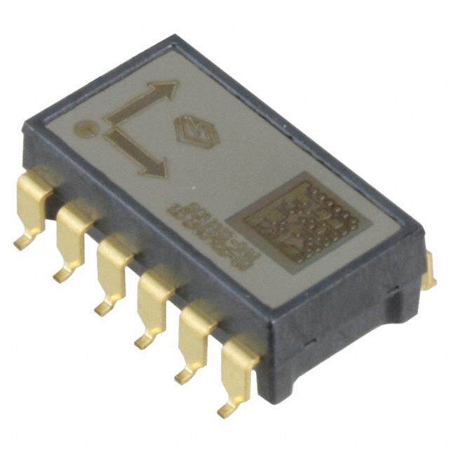
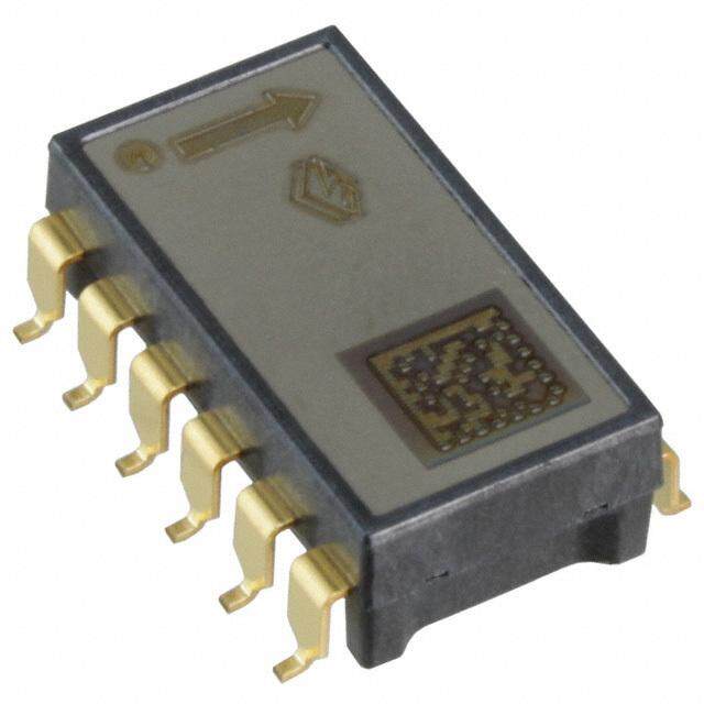
| 描述 | 加速计 IC 360 Degree Inclinometer |
| 产品分类 | 运动与定位传感器 |
| 产品手册 | |
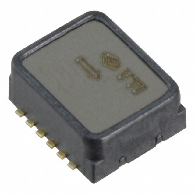
| 产品图片 |
|
| rohs | RoHS 合规性豁免 |
| 产品系列 | 加速计,Analog Devices ADIS16203CCCZ |
| 产品型号 | ADIS16203CCCZ |
| PCN设计/规格 | |
| 产品培训模块 | http://www.digikey.cn/PTM/IndividualPTM.page?site=cn&lang=zhs&ptm=38 |
| 产品目录页面 | |
| 产品种类 | 加速计 |
| 分辨率 | 14 bit |
| 加速 | 3500 g |
| 商标 | Analog Devices |
| 安装风格 | SMD/SMT |
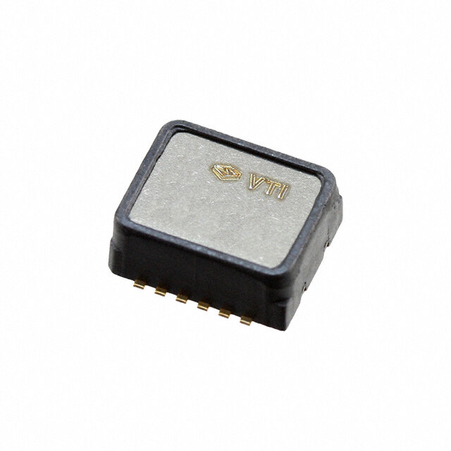
| 封装 | Tray |
| 封装/外壳 | 16-LGA |
| 封装/箱体 | LGA-16 |
| 工厂包装数量 | 168 |
| 带宽 | 2.25kHz |
| 接口 | SPI |
| 数字输出-位数 | 14 bit |
| 数字输出-总线接口 | SPI |
| 最大工作温度 | + 125 C |
| 最小工作温度 | - 40 C |
| 标准包装 | 1 |
| 测量范围 | ±360° |
| 灵敏度 | 0.025 LSB |
| 电源电压-最大 | 3.6 V |
| 电源电压-最小 | 3 V |
| 电源电流 | 11 uA |
| 系列 | ADIS16203 |
| 轴 | X 或 Y |
| 输出类型 | Digital |
| 配用 | /product-detail/zh/ADIS16203%2FPCBZ/ADIS16203%2FPCBZ-ND/1166711 |
| 额定电压 | 3 V ~ 3.6 V |


- 商务部:美国ITC正式对集成电路等产品启动337调查
- 曝三星4nm工艺存在良率问题 高通将骁龙8 Gen1或转产台积电
- 太阳诱电将投资9.5亿元在常州建新厂生产MLCC 预计2023年完工
- 英特尔发布欧洲新工厂建设计划 深化IDM 2.0 战略
- 台积电先进制程称霸业界 有大客户加持明年业绩稳了
- 达到5530亿美元!SIA预计今年全球半导体销售额将创下新高
- 英特尔拟将自动驾驶子公司Mobileye上市 估值或超500亿美元
- 三星加码芯片和SET,合并消费电子和移动部门,撤换高东真等 CEO
- 三星电子宣布重大人事变动 还合并消费电子和移动部门
- 海关总署:前11个月进口集成电路产品价值2.52万亿元 增长14.8%

PDF Datasheet 数据手册内容提取
Programmable 360° Inclinometer Data Sheet ADIS16203 FEATURES ADIS16203 provides factory-calibrated, sensor-to-digital incline- 0° to 360° Inclinometer angle data in a convenient format that can be accessed using a ±180 output format option serial peripheral interface (SPI). The SPI interface provides access 14-bit digital inclination outputs to multiple measurements: 360° linear inclination angles, ±180° Linear output, 0.025° resolution linear incline angles, temperature, power supply, and one auxiliary 12-bit digital temperature sensor output analog input. Easy access to calibrated digital sensor data provides Digitally controlled bias calibration developers with a system-ready device, reducing development Digitally controlled sample rate time, cost, and program risk. Digitally controlled filtering Unique characteristics of the end system are accommodated Digitally controlled direction/orientation easily through several built-in features, such as a single-command Dual alarm settings with rate/threshold limits offset calibration, along with convenient sample rate and band- Auxiliary digital I/O width control. Digitally activated self-test Digitally activated low power mode The ADIS16203 offers the following embedded features that SPI®-compatible serial interface eliminate the need for external circuitry and provide a simplified Auxiliary 12-bit ADC input and DAC output system interface: Single-supply operation: 3.0 V to 3.6 V Configurable alarm function 3500 g powered shock survivability Auxiliary 12-bit analog-to-digital converter (ADC) APPLICATIONS Auxiliary 12-bit digital-to-analog converter (DAC) Tilt sensing, inclinometers Platform control, stabilization, and leveling Configurable digital I/O port Motion/position measurement Digital self-test function Monitor/alarm devices (security, medical, safety) The ADIS16203 offers two power management features for Robotics managing system-level power dissipation: low power mode and GENERAL DESCRIPTION a configurable shutdown feature. The ADIS16203 is a complete incline-angle measurement system in The ADIS16203 is available in a 9.2 mm × 9.2 mm × 3.9 mm a single compact package enabled by the Analog Devices, Inc., laminate-based land grid array (LGA) package with a temper- iSensor™ integration. By enhancing the Analog Devices iMEMS® ature range of −40°C to +125°C. sensor technology with an embedded signal processing solution, the FUNCTIONAL BLOCK DIAGRAM AUX AUX ADC DAC VREF ADIS16203 TEMPERATURE SENSOR CS SIGNAL CALIBRATION INERTIAL CONDITIONING AND MEMS AND DIGITAL SCLK SENSOR CONVERSION PROCESSING SPI PORT DIN SELF-TEST CDOIGNTITRAOLL DOUT VDD MANPAOGWEEMRENT ALARMS AUXII/LOIARY COM AUX COM RST DIO0 DIO1 06108-001 Figure 1. Rev. B Document Feedback Information furnished by Analog Devices is believed to be accurate and reliable. However, no responsibility is assumed by Analog Devices for its use, nor for any infringements of patents or other One Technology Way, P.O. Box 9106, Norwood, MA 02062-9106, U.S.A. rights of third parties that may result from its use. Specifications subject to change without notice. No license is granted by implication or otherwise under any patent or patent rights of Analog Devices. Tel: 781.329.4700 ©2006–2018 Analog Devices, Inc. All rights reserved. Trademarks and registered trademarks are the property of their respective owners. Technical Support www.analog.com
ADIS16203 Data Sheet TABLE OF CONTENTS Features .............................................................................................. 1 Calibration Register Definition ................................................ 15 Applications ....................................................................................... 1 Alarms .......................................................................................... 15 General Description ......................................................................... 1 Sample Period Control .............................................................. 18 Functional Block Diagram .............................................................. 1 Filtering Control ......................................................................... 18 Revision History ............................................................................... 2 Power-Down Control ................................................................ 19 Specifications ..................................................................................... 3 Status Feedback........................................................................... 20 Timing Specifications .................................................................. 5 COMMAND Control ................................................................ 20 Timing Diagrams .......................................................................... 5 Miscellaneous Control Register................................................ 21 Absolute Maximum Ratings ............................................................ 6 Peripherals ....................................................................................... 22 ESD Caution .................................................................................. 6 Auxiliary ADC Function ........................................................... 22 Pin Configuration and Function Descriptions ............................. 7 Auxiliary DAC Function ........................................................... 22 Typical Performace Characteristics ................................................ 8 General-Purpose I/O Control .................................................. 23 Theory of Operation ...................................................................... 11 Applications Information .............................................................. 24 Output Response ........................................................................ 11 Hardware Considerations ......................................................... 24 Temperature Sensor ................................................................... 11 Grounding and Board Layout Recommendations ................. 24 Basic Operation ............................................................................... 12 Self-Test Tips ............................................................................... 24 Serial Peripheral Interface (SPI) ............................................... 12 Band Gap Reference ................................................................... 24 Data Output Register Access ..................................................... 13 Power Supply Considerations ................................................... 25 Programming and Control ............................................................ 14 Assembly ...................................................................................... 25 Control Register Overview ........................................................ 14 Example Pad Layout ................................................................... 25 Control Register Access ............................................................. 14 Outline Dimensions ....................................................................... 26 Control Register Details................................................................. 15 Ordering Guide .......................................................................... 26 Calibration ................................................................................... 15 REVISION HISTORY 1/2010—Rev. 0 to Rev. A 7/2018—Rev. A to Rev. B Changes to Figure 25 ...................................................................... 11 Changed Applications Section to Applications Information Changes to Table 19 ........................................................................ 20 Section .............................................................................................. 24 Changes to Table 23 ........................................................................ 21 Deleted Power-On Reset Operation Section, Figure 33, Second- Updated Outline Dimensions ........................................................ 26 Level Assembly Section, Figure 34, and Table 24; Renumbered Sequentially ..................................................................................... 25 8/2006—Revision 0: Initial Version Added Power Supply Considerations Section, Power-On-Reset Function Section, Transient Current from VDD Ramp Rate Section, and Assembly Section ..................................................... 25 Rev. B | Page 2 of 28
Data Sheet ADIS16203 SPECIFICATIONS T = −40oC to +125°C, VDD = 3.3 V, tilt = 0°, unless otherwise noted. A Table 1. Parameter Conditions Min Typ Max Unit INCLINOMETER1 Input Range 360 Degrees Relative Accuracy 25°C, maximum filter setting ±0.6 Degrees Sensitivity 25°C 0.025 Degrees/LSB Accuracy Temperature Coefficient ±0.0167 Degrees/°C NOISE PERFORMANCE Output Noise At 25°C, no averaging 1.0 Degrees rms At 25°C, maximum averaging 0.1 Degrees rms Noise Density At 25°C, no averaging 0.037 Degrees/√Hz rms FREQUENCY RESPONSE Sensor Bandwidth 2250 Hz Sensor Resonant Frequency 5.5 kHz SELF-TEST STATE Output Change When Active At 25°C 34 Degrees TEMPERATURE SENSOR Output at 25°C 1278 LSB Scale Factor −2.13 LSB/°C ADC INPUT Resolution 12 Bits Integral Nonlinearity ±2 LSB Differential Nonlinearity ±1 LSB Offset Error ±4 LSB Gain Error ±2 LSB Input Range 0 2.5 V Input Capacitance During acquisition 20 pF ON-CHIP VOLTAGE REFERENCE 2.5 V Accuracy At 25°C −10 +10 mV Reference Temperature Coefficient ±40 ppm/°C Output Impedance 70 Ω DAC OUTPUT 5 kΩ/100 pF to GND Resolution 12 Bits Relative Accuracy For Code 101 to Code 4095 4 LSB Differential Nonlinearity 1 LSB Offset Error ±5 mV Gain Error ±0.5 % Output Range 0 to 2.5 V Output Impedance 2 Ω Output Settling Time 10 μs LOGIC INPUTS Input High Voltage, V 2.0 V INH Input Low Voltage, V 0.8 V INL Logic 1 Input Current, I V = VDD ±0.2 ±1 μA INH IH Logic 0 Input Current, I V = 0 V −40 −60 μA INL IL Input Capacitance, C 10 pF IN DIGITAL OUTPUTS Output High Voltage, V I = 1.6 mA 2.4 V OH SOURCE Output Low Voltage, V I = 1.6 mA 0.4 V OL SINK Rev. B | Page 3 of 28
ADIS16203 Data Sheet Parameter Conditions Min Typ Max Unit SLEEP TIMER Timeout Period2 0.5 128 Seconds FLASH MEMORY Endurance3 20,000 Cycles Data Retention4 T = 85°C 20 Years J CONVERSION RATE Minimum Conversion Time 244 μs Maximum Conversion Time 484 ms Maximum Throughput Rate 4096 SPS Minimum Throughput Rate 2.066 SPS POWER SUPPLY Operating Voltage Range VDD 3.0 3.3 3.6 V Power Supply Current Normal mode, SMPL_TIME ≥ 0x08 11 14 mA (fS ≤ 910 Hz) at 25°C Fast mode, SMPL_TIME ≤ 0x07 36 42 mA (f ≥ 1024 Hz) at 25°C S Sleep mode at 25°C 500 750 μA Turn-On Time 130 ms 1 This sensor relies on the earth’s gravity to provide accurate incline angle measurements. The axis of rotation must be perpendicular to the earth’s gravity to maintain the factory-calibrated accuracy of the sensor. 2 Guaranteed by design. 3 Endurance is qualified as per JEDEC Standard 22 Method A117 and measured at −40°C, +25°C, +85°C, and +125°C. 4 Retention lifetime equivalent at junction temperature (TJ) 55°C as per JEDEC Standard 22 Method A117. Retention lifetime decreases with junction temperature. Rev. B | Page 4 of 28
Data Sheet ADIS16203 TIMING SPECIFICATIONS T = +25°C, VDD = 3.3 V, tilt = 0°, unless otherwise noted. A Table 2. Parameter Description Min1 Typ Max Unit f Fast mode, SMPL_TIME ≤ 0x07 (f ≥ 1024 Hz) 0.01 2.5 MHz SCLK S Normal mode, SMPL_TIME ≥ 0x08 (f ≤ 910 Hz) 0.01 1.0 MHz S t Chip select period, fast mode, SMPL_TIME ≤ 0x07 (f ≥ 1024 Hz) 40 μs DATARATE S Chip select period, normal mode, SMPL_TIME ≥ 0x08 (f ≤ 910 Hz) 100 μs S t Chip select to clock edge 48.8 ns CS t Data output valid after SCLK falling edge2 100 ns DAV t Data input setup time before SCLK rising edge 24.4 ns DSU t Data input hold time after SCLK rising edge 48.8 ns DHD t Data output fall time 5 12.5 ns DF t Data output rise time 5 12.5 ns DR t CS high after SCLK edge3 5 ns SFS 1 Guaranteed by design, not production tested. 2 The MSB presents an exception to this parameter. The MSB clocks out on the falling edge of CS. The rest of the DOUT bits are clocked after the falling edge of SCLK and are governed by this specification. 3 This parameter may need to be expanded to allow for proper capture of the LSB. After CS goes high, the DOUT line goes into a high impedance state. TIMING DIAGRAMS tDATARATE tSTALL CS SCLK tSTALL =tDATARATE – 16/fSCLK 06108-002 Figure 2. SPI Chip Select Timing CS tCS tSFS 1 2 3 4 5 6 15 16 SCLK tDAV DOUT MSB DB14 DB13 DB12 DB11 DB10 DB2 DB1 LSB tDSU tDHD DIN W/R A5 A4 A3 A2 D2 D1 LSB 06108-003 Figure 3. SPI Timing, Utilizing SPI Settings Typically Identified as Phase = 1, Polarity = 1 Rev. B | Page 5 of 28
ADIS16203 Data Sheet ABSOLUTE MAXIMUM RATINGS Table 3. Stresses at or above those listed under Absolute Maximum Parameter Rating Ratings may cause permanent damage to the product. This is a Acceleration (Any Axis, Unpowered) 3500 g stress rating only; functional operation of the product at these Acceleration (Any Axis, Powered) 3500 g or any other conditions above those indicated in the operational VDD to COM −0.3 V to +7.0 V section of this specification is not implied. Operation beyond Digital Input/Output Voltage to COM −0.3 V to +5.5 V the maximum operating conditions for extended periods may Analog Inputs to COM −0.3 V to VDD + 0.3 V affect product reliability. Operating Temperature Range −40°C to +125°C Table 4. Package Characteristics Storage Temperature Range −65°C to +150°C Package Type θ θ Device Weight JA JC 16-Terminal LGA 250°C/W 25°C/W 0.6 g ESD CAUTION Rev. B | Page 6 of 28
Data Sheet ADIS16203 PIN CONFIGURATION AND FUNCTION DESCRIPTIONS C D D AX EF M D U R O V A V C 13 14 15 16 AUX DAC 12 1 SCLK ADIS16203 NC 11 2 DOUT BOTTOM VIEW AUX COM 10 (Not to Scale) 3 DIN RST 9 4 CS 8 7 6 5 NC = NO CONNECT OMAUXC NC DOI1 DO0I 06108-004 Figure 4. Pin Configuration Table 5. Pin Function Descriptions Pin No. Mnemonic Type1 Description 1 SCLK I SPI Serial Clock. 2 DOUT O SPI Data Out. 3 DIN I SPI Data In. 4 CS I SPI Chip Select, Active Low. This input frames the serial data transfer. 5, 6 DIO0, DIO1 I/O Multifunction Digital I/O Pin. 7, 11 NC – No Connect. 8, 10 AUX COM S Auxiliary Grounds. Connect to GND for proper operation. 9 RST I Reset, Active Low. This input resets the embedded microcontroller to a known state. 12 AUX DAC O Auxiliary DAC Analog Voltage Output. 13 VDD S +3.3 V Power Supply. 14 AUX ADC I Auxiliary ADC Analog Input Voltage. 15 VREF O Precision Reference Output. 16 COM S Common. Reference point for all circuitry in the ADIS16203. 1 S = supply, O = output, I = input. Rev. B | Page 7 of 28
ADIS16203 Data Sheet TYPICAL PERFORMACE CHARACTERISTICS 30 90 25 80 70 N (%) 20 ees) 60 O gr POPULATI 1150 CL_OUT (De 5400 N 30 I 5 20 10 0 –1.0 –0.8 –0.6 –0.4E–R0R.2OR (0Degre0e.2s) 0.4 0.6 0.8 1.0 06108-032 02.9 3.0 3.1 3.2SUPP3.L3Y (V)3.4 3.5 3.6 3.7 06108-008 Figure 5. Inclination Error Distribution at 25°C/3.3 V, Incline = 0° Figure 8. Self-Test Shift vs. Supply at 25°C 150 3.5 3.0 125 2.5 100 ees) 2.0 TY gr TI De 1.5 AN 75 UT ( QU O 1.0 _ 50 L C N 0.5 I 0 25 –0.5 0 6802468024680246802468024 –1.0–40 –20 0 T2E0MPER4A0TURE6 (0°C) 80 100 120 06108-006 607.607.608.608.608.608.608.609.609.609.609.(µ609.V/610.LS610.B)610.610.610.611.611.611.611.611.612.612.612. 06108-009 Figure 6. Inclination Error vs. Temperature Figure 9. ADC Gain Distribution at 25°C/3.3 V 80 0.40 70 0.35 60 0.30 s) 50 gree 0.25 TITY OR (De 0.20 QUAN 40 R 30 R 0.15 E ± 20 0.10 10 0.05 0 02.9 3.0 3.1 SU3P.2PLY V3O.3LTAG3E. 4(V) 3.5 3.6 3.7 06108-033 –2.4–2.1–1.8–1.5–1.2–0.9–0.6–0.300.30.60.9(m1.2V)1.51.82.12.42.73.03.33.63.94.24.54.8 06108-010 Figure 7. Inclination Error vs. Supply Figure 10. ADC Offset Distribution at 25°C/3.3 V Rev. B | Page 8 of 28
Data Sheet ADIS16203 3 45 40 2 35 B) S 1 30 L LINEARITY ( 0 QUANTITY 2250 N O –1 15 N 10 –2 5 –3 0 1 4096 ADC8 C19O2DES 12288 16384 06108-011 –2.7–2.4–2.1–1.8–1.5–1.2–0.9–0.6–0.300.30.6(m0.9V)1.21.51.82.12.42.73.03.33.63.94.24.5 06108-014 Figure 11. Typical ADC Integral Nonlinearity at 25°C/3.3 V Figure 14. DAC Offset Distribution at 25°C/3.3 V 3 5 3.0V/–40°C 3.0V/+25°C 4 3.0V/+125°C 2 3.3V /–40°C 3 3.3V/+25°C 3.3V/+125°C SB) 1 SB) 2 33..66VV//–+4205°°CC Y (L Y (L 1 3.6V/+125°C ARIT 0 ARIT 0 E E N N NLI NLI –1 O –1 O N N –2 –3 –2 –4 –31 4096 ADC8 C19O2DES 12288 16384 06108-012 –50 512 1024 1536DAC2 C04O8DES2560 3072 3584 4096 06108-015 Figure 12. Typical ADC Differential Nonlinearity Figure 15. Typical DAC Integral Nonlinearity 120 250 100 200 80 QUANTITY 60 QUANTITY 115000 40 50 20 0 0 606.6606.9607.2607.5607.8608.1608.4608.7609.0609.3609.6(µ609.9V/610.2LS610.5B)610.8611.1611.4611.7612.0612.3612.6612.9613.2613.5613.8 06108-013 2.49752.49772.49792.49812.49832.49852.49872.49892.49912.49932.49952.4997(V2.4999)2.50012.50032.50052.50072.50092.50112.50132.50152.50172.50192.50212.5023 06108-016 Figure 13. DAC Gain Distribution at 25°C/3.3 V Figure 16. VREF Distribution at 25°C/3.3 V Rev. B | Page 9 of 28
ADIS16203 Data Sheet 60 180 160 50 140 40 120 Y Y TIT TIT 100 N 30 N A A U U 80 Q Q 20 60 40 10 20 0 0 55667788990011223344556677 0864208642086420864208642 111111111122(2°C2) 222222222222 06108-017 373738394041414243444545(µ46A)474849495051525353545556 06108-020 Figure 17. Temperature Distribution at 25°C/3.3 V Figure 20. Sleep Mode Power Supply Current Distribution at 25°C/3.3 V 140 0.0010 120 0.0008 100 A) T ( N Y E NTIT 80 URR0.0006 A C QU 60 DE O M0.0004 40 EP E L S 20 0.0002 0 9.4 9.7 10.0 10.3 10.6 10.9(m11.2A) 11.5 11.8 12.1 12.4 12.7 13.0 06108-018 0–50 –30 –10 10 TE3M0PERA50TURE7 0(°C) 90 110 130 150 06108-021 Figure 18. Normal Mode Power Supply Current Distribution at 25°C/3.3 V Figure 21. Sleep Mode Current vs. Temperature at 3.3 V 140 0.0010 120 0.0008 100 A) T ( N QUANTITY 8600 DE CURRE0.0006 O M0.0004 P 40 E E L S 20 0.0002 0 29.029.630.230.831.432.032.633.233.834.435.035.6(m36.2A)36.837.438.038.639.239.840.441.041.642.242.843.4 06108-019 02.9 3.0 3.1 SU3P.2PLY V3O.3LTAG3E. 4(V) 3.5 3.6 3.7 06108-022 Figure 19. Fast Mode Power Supply Current Distribution at 25°C/3.3 V Figure 22. Sleep Mode Current vs. Supply Voltage at 25°C Rev. B | Page 10 of 28
Data Sheet ADIS16203 THEORY OF OPERATION The ADIS16203 is a calibrated digital inclinometer that provides a OUTPUT RESPONSE full 360° of measurement range in any rotational plane that is parallel to The incline-angle measurements are linear with respect to the earth’s gravity. A dual-axis accelerometer provides the base-sensing degrees, and the sensor’s orientation produces the output function, which resolves the earth’s gravity into two orthogonal vectors, response displayed in Figure 25. This figure is helpful in as displayed in Figure 23. A power-efficient approach to a common understanding the basic orientation of the inertial sensor trigonometric identity converts these orthogonal vectors into an incline- measurement axes. angle measurement. INCL_OUT = +270° INCL_180_OUT = –90° 1g INCL_OUT = 0° INCL_180_OUT = 0° a2 1g a1 BOTTOM 0° VIEW (Not to Scale) EARTH’S SURFACE 06108-036 INCL_OUT = 180° Figure 23. Sensor Measurement Diagram INCL_180_OUT = 180° The digital postprocessing circuit digitizes the sensor outputs and applies sensitivity/offset calibration coefficients prior to angle calculations. A factory calibration produces these coefficients using INCL_OUT = 90° a full 360° mechanical rotational apparatus. This eliminates the need INCL_180_OUT = 90° for system-level calibration in many cases. In addition to calibrating EARTH’S SURFACE tdheep esenndseonrt epleamraemnettse, rtsh,e p AroDvIidSi1n6g2 0a 3m coorrer ercotbs ufostr cpaoliwberar-tisounp.p ly- 06108-023 Figure 25. Output Response vs. Orientation The accuracy of the incline-angle measurements relies on three TEMPERATURE SENSOR important factors: the absence of external (aside from gravity) An internal temperature sensor monitors the accelerometer’s acceleration, managing offset errors introduced during system-level junction temperature. The TEMP_OUT data register provides a configuration, and maintaining a proper axis of rotation (rotation digital representation of this measurement. This sensor provides a plane parallel with earth’s gravity). All of these factors can influence convenient temperature measurement for system-level charac- the acceleration measurements and introduce error. The ADIS16203 terization and calibration feedback. provides a simple method for calibrating configuration errors by providing the INCL_NULL register function. See the Calibration section for more details. In addition, a 10° tilt plane error can introduce as much as ±1° of error in the incline-angle outputs. SYSTEM-LEVEL ORIENTATION OFFSET TILT PLANE ERROR PCB ATTACHMENT IDEAL = 90° OFFSET EARTH’S SURFACE 06108-038 Figure 24. ADIS16203 System-Level Orientation Rev. B | Page 11 of 28
ADIS16203 Data Sheet BASIC OPERATION have no impact on operation. A complete data frame contains 16 The ADIS16203 is designed for simple integration into industrial clock cycles. Because the SPI port operates in full duplex mode, it system designs, requiring only a 3.3 V power supply and a 4-wire, supports simultaneous, 16-bit receive (DIN) and transmit (DOUT) industry standard SPI. The SPI port facilitates all data transfers functions during the same data frame. with the ADIS16203’s registers. Each ADIS16203 function (output data and programming control) has its own register that contains Figure 26 displays a typical data frame for writing a command to a two bytes of data, and each byte of data has its own unique bit control register. In this case, the first bit of the DIN sequence is a map. These two bytes are referred to as upper and lower bytes, and 1, followed by a 0, then the 6-bit address and 8-bit data command. each has its own 6-bit address. Because each write command covers a single byte of data, two data SERIAL PERIPHERAL INTERFACE (SPI) frames are required when writing the entire 16-bit space of a register. The ADIS16203’s SPI port provides a common interface that is Reading the contents of a register requires a modification to the supported by a wide variety of digital platforms, including MCUs, sequence in Figure 26. In this case, the first two bits in the DIN DSPs, and FPGAs. Even when a dedicated port is not available, the sequence are 0, followed by the address of the register. Each register SPI can be implemented using manual bit manipulation, which is has two addresses, but either one can be used to access its entire more commonly known as bit banging. The purpose of this section is 16 bits of data. The final eight bits of the DIN sequence are irrelevant to provide a basic description of SPI operation in the ADIS16203. and can be counted as don’t cares during a read command. Then, Please refer to Table 2, Figure 2, and Figure 3 for detailed timing during the next data frame, the DOUT sequence will contain the and operation of this port. register’s 16-bit data, as shown in Figure 27. Even though a single read command requires two separate data frames, the full duplex The ADIS16203’s SPI port includes four signals: chip select (CS), mode minimizes this overhead, requiring only one extra data frame serial clock (SCLK), data input (DIN), and data output (DOUT). when continuously sampling. The CS line enables the ADIS16203’s SPI port and, in effect, frames each SPI event. When this signal is high, the DOUT lines are in a high impedance state and the signals on DIN and SCLK DATA FRAME CS SCLK DIN W/R A5 A4 A3 A2 A1 A0 DC7 DC6 DC5 DC4 DC3 DC2 DC1 DC0 WRERAITDE == 01 REGISTER ADDRESS DOND’ATT CAA FROER F WORR IRTEE ACDO CMOMMAMNDASNDS 06108-037 Figure 26. DIN Bit Sequence CS DATA FRAME DATA FRAME SCLK DIN ADDRESS DON’T CARE NEXT COMMAND W/R BIT ZERO DOUT BASED ON PREVIOUS COMMAND 16-BIT REGISTER CONTENTS 06108-024 Figure 27. SPI Sequence for Read Commands Rev. B | Page 12 of 28
Data Sheet ADIS16203 DATA OUTPUT REGISTER ACCESS The MSB holds the new data (ND) indicator. When the output registers are updated with new data, the ND bit goes to a 1 state. The ADIS16203 provides access to two calibrated incline-angle After the output data is read, it returns to a 0 state. The EA bit is measurements (+360° and ±180° output formats), power supply used to indicate an alarm condition, which could result from a measurements, temperature measurements, and an auxiliary number of conditions, such as a power supply that is out of the 12-bit ADC channel. This output data is continuously updating specified operating range. See the Alarms section for more details. internally, regardless of user read rates. The follow bit map describes the structure of all output data registers in the ADIS16203. The output data is either 12 or 14 bits in length. For all of the 12-bit MSB LSB output data, the D13 and D12 bits are assigned don’t care status. ND EA D13 D12 D11 D10 D9 D8 The output data register map is located in Table 6 and provides all D7 D6 D5 D4 D3 D2 D1 D0 of the necessary details for accessing each register’s data. Table 7 displays the output coding for the ±180° output data register, INCL_180_OUT, and Figure 28 displays a timing diagram example for reading this register. Table 6. Data Output Register Information Resolution Data Scale Factor Name Function Address (Bits) Format (per LSB) SUPPLY_OUT Power supply data 0x03, 0x02 12 Binary 1.22 mV AUX_ADC Auxiliary analog input data 0x09, 0x08 12 Binary 0.61 mV TEMP_OUT Sensor temperature data 0x0B, 0x0A 12 Binary −0.47°C INCL_OUT Inclination data 0x0D, 0x0C 14 Binary 0.025° INCL_180_OUT ±180° inclination data 0x0F, 0x0E 14 Twos complement 0.025° Table 7. Output Coding Example, INCL_180_OUT1, 2 Acceleration Level Binary Output Hex Output Decimal +170.10° 01 1010 1001 0100 0x1A94 +6804 +93.05° 00 1110 1000 1010 0x0E8A +3722 +0.625° 00 0000 0001 1001 0x0019 +25 0.00° 00 0000 0000 0000 0x0000 0 −0.625 11 1111 1110 0111 0x3FE7 −25 −93.05° 11 0001 0111 0110 0x3176 −3722 −170.10° 11 1100 0001 1000 0x256C −6804 1 Two MSBs have been masked off and are not considered in the coding. 2 Nominal sensitivity (0.025°/LSB) and zero offset null performance are assumed. CS SCLK DIN W/R BIT = 0 ADDRESS = 001111 W/R BIT = 0 ADDRESS = 001111 OR 0x0F DOUT DNAEWTA D =A 1T0A0,0 N11O1 0A1L0A0R01M0,1 I0NCL_180_OUT = +93.05° 06108-025 Figure 28. SPI Sequence Reading INCL_OUT When Incline Angle = 93.05° Rev. B | Page 13 of 28
ADIS16203 Data Sheet PROGRAMMING AND CONTROL CONTROL REGISTER OVERVIEW CONTROL REGISTER ACCESS The ADIS16203 offers many programmable features that are Table 8 displays the control register map for the ADIS16203, controlled by writing commands to the appropriate control registers including address, volatile status, basic function, and accessibility using the SPI. For added system flexibility and programmability, (read/write). The following sections contain detailed descriptions the following sections describe these controls and specify each and configurations for each of these registers. register’s configuration. A list of features that are available for The ADIS16203 is a Flash-based device with the nonvolatile configuration in this register space follows: functional registers implemented as Flash registers. Take into Calibration: Automatic offset null, manual offset adjustment, account the endurance limitation of 20,000 writes when consid- factory reset ering the system-level integration of these devices. The nonvolatile column in Table 8 indicates the registers that are recovered on power- Rotational direction: clockwise or counter-clockwise up. The user must use a manual Flash update command (using the command register) to store the nonvolatile data registers once they Sample rate adjustment are configured properly. When performing a manual Flash update Filter response optimization command, the user needs to ensure that the power supply remains within limits for a minimum of 50 ms after the start of the update. Alarm settings: threshold or rate of change, and comparison This ensures a successful write of the nonvolatile data. with filtered or unfiltered data I/O configuration: data ready, etc. Power management: sleep mode, normal and high performance modes Auxiliary DAC level setting Status checks: verify power supply, SPI communication, package orientation Flash™ updates to store configuration Table 8. Control Register Mapping Register Name Type Nonvolatile Address Bytes Function 0x00 to 0x01 2 Reserved INCL_NULL R/W X 0x18 2 Incline null calibration ALM_MAG1 R/W X 0x20 2 Alarm 1 amplitude threshold ALM_MAG2 R/W X 0x22 2 Alarm 2 amplitude threshold ALM_SMPL1 R/W X 0x24 2 Alarm 1 sample period ALM_SMPL2 R/W X 0x26 2 Alarm 2 sample period ALM_CTRL R/W X 0x28 2 Alarm source control register 0x2A to 0x2F 6 Reserved AUX_DAC R/W 0x30 2 Auxiliary DAC data GPIO_CTRL R/W 0x32 2 Auxiliary digital I/O control register MSC_CTRL R/W X 0x34 2 Miscellaneous control register SMPL_TIME R/W X 0x36 2 ADC sample period control AVG_CNT R/W X 0x38 2 Defines number of samples used by moving average filter SLP_CNT R/W 0x3A 2 Counter used to determine length of power-down mode STATUS R 0x3C 2 System status register COMMAND W 0x3E 2 System command register Rev. B | Page 14 of 28
Data Sheet ADIS16203 CONTROL REGISTER DETAILS All ADIS16203 control registers are organized into 2-byte segments, CALIBRATION REGISTER DEFINITION and both upper (Bit 8 to Bit 15) and lower (Bit 0 to Bit 7) bytes have INCL_NULL Register Definition unique addresses and can be accessed individually. Address Scale1 Default Format Access MSB LSB 0x19, 0x18 0.025° 0x0000 Binary R/W D15 D14 D13 D12 D11 D10 D9 D8 1 Scale is the weight of each LSB. D7 D6 D5 D4 D3 D2 D1 D0 The INCL_NULL register is the user controlled register for This section provides a description of each register, including its calibrating system-level inclination offset errors. The maximum purpose, relevant scaling information, bit maps, addresses, and calibration range is +0° to +359.975° or 0 to +14,399 decimal default values. codes. The contents of this register are nonvolatile. CALIBRATION Table 10. INCL_NULL Bit Designations In addition to the factory calibration, the ADIS16203 provides two Bit Description user calibration options. Both options utilize the INCL_NULL 15:14 Not necessary, force to 0 control register, which provides an add function to the two incline- 13:0 Data bits angle output registers: INCL_OUT and INCL_180_OUT. Because the default contents of INCL_NULL are 0, adding it to these two ALARMS outputs has no effect on the output data. The ADIS16203 contains two independent alarm functions that The first calibration option is an automatic null function. This function are referred to as Alarm 1 and Alarm 2. The Alarm 1 function is measures the contents of INCL_OUT and then writes the inverse of managed by the ALM_MAG1 and ALM_SMPL1 control registers. this value into the INCL_NULL control register. The accuracy of this The Alarm 2 function is managed by the ALM_MAG2 and calibration is dependent on the stability of the INCL_OUT measure- ALM_SMPL2 control registers. Both the Alarm 1 and Alarm 2 ment; therefore, maximizing the filtering will minimize the errors functions share the ALM_CTRL register. For simplicity, this associated with noise. Table 9 displays a sequence that executes the section refers to the Alarm 1 functionality only. automatic null. The 16-bit ALM_CTRL register serves several roles in controlling Table 9. Automatic Null Sequence the Alarm 1 function. First, it is used to enable the overall Alarm 1 Step Description function and to select the output data variable that is to be Write 0x08 to Address 0x38 Sets averaging count to 256 monitored for the alarm condition. Second, it is used to select using the AVG_CNT register whether the Alarm 1 function is based upon a predefined threshold Wait for 512 samples Waits for the lowest noise data (THR) level or a predefined rate-of-change (ROC) slope. Third, Write 0x01 to Address 0x3E Executes the global autonull the ALM_CTRL register can be used in setting up one of the function using the COMMAND register two general-purpose input/output lines (GPIOs) to serve as a Restore previous average count hardware output that indicates when an alarm condition has occurred. Enabling the I/O alarm function as well as setting its polarity and controlling its operation are accomplished using Increasing the sample rate using the SMPL_TIME control register this register. Fourth, this register provides the controls for will minimize the waiting time if this parameter is critical. setting the comparison data as filtered or unfiltered. The second option for system-level calibration is manual adjustment. Note that when enabled, the hardware output indicator serves The INCL_NULL control register can be updated using write com- both the Alarm 1 and Alarm 2 functions and cannot be used to mands. Refer to its definition in the INCL_NULL Register Definition differentiate between one alarm condition and the other. It is section for details. simply used to indicate that an alarm is active and that the user The factory calibration can be restored by writing 0x02 to Register should poll the device via the SPI to determine the source of the Address 0x3E. This restores INCL_NULL to 0. alarm condition (see the STATUS Register Definition section). Because the ALM_CTRL, MSC_CTRL, and GPIO_CTRL control registers can influence the same GPIO pins, a priority level has been established to avoid conflicting assignments of the two GPIO pins. This priority level is defined as MSC_CTRL, which has precedence over ALM_CTRL, which has precedence over GPIO_CTRL. Rev. B | Page 15 of 28
ADIS16203 Data Sheet The ALM_MAG1 control register used in controlling the Alarm 1 Bits 4 and 5 in the ALM_CTRL register establishes whether function has two roles. The first role is to store the value with which ALM_MAG1 and ALM_MAG2 are compared with filtered or the output data variable is compared against to discern if an alarm unfiltered data. condition exists. The second role is to identify whether the alarm should be active for excursions above or below the alarm limit. If 1 is ALM_MAG1 Register Definition written to Bit 15 of the ALM_MAG1 control register, the alarm is Address Default1 Format2 Access active for excursions extending above a given limit. If 0 is written to 0x21, 0x20 0x0000 N/A R/W Bit 15, the alarm is active for excursions dropping below the given 1 Default is valid only until the first register write cycle. limit. The comparison value contained within the ALM_MAG1 2 Format is established by source of monitored data control register is located within the lower 14 bits. The monitored output register establishes the format of the 14-bit The ALM_MAG1 register contains the threshold level for data space in the ALM_MAG1 and ALM_MAG2 registers. For Alarm 1. The contents of this register are nonvolatile. example, setting the alarm to monitor INCL_OUT sets the data Table 11. ALM_MAG1 Bit Designations format to a 14-bit, twos complement number, which carries a bit Bit Description weight of 0.025°. 15 Greater than Active Alarm Bit. 1: Alarm is active for an output greater than Use caution when monitoring the temperature output register for the ALM_MAG1 register setting. alarm conditions. Here, the negative temperature scale factor results 0: Alarm is active for an output less than in the greater than and less than selections requiring reverse logic. ALM_MAG1 register setting. 14 Not used. Setting Bit 11 in the ALM_CTRL register establishes the mode of 13:0 Data Bits. This number can be either twos complement operation: threshold or rate of change (ROC). When the ROC or straight binary. The format is set by the value being function is enabled, the comparison of the output data variable is monitored by this function. against the ALM_MAG1 level averaged over the number of samples as identified in the ALM_SMPL1 control register. This acts to create ALM_SMPL1 Register Definition a comparison of (Δ units/Δ time) or the derivative of the output data Address Default1 Format Access variable against a predefined slope. 0x25, 0x24 0x0000 Binary R/W The versatility built into the alarm function allows the user to adapt 1 Default is valid only until the first register write cycle. to several applications. For example, in the case of monitoring twos complement variables, Bit 15 within the ALM_MAG1 control register can allow for the detection of negative excursions below a fixed level. The ALM_SMPL1 register contains the sample period information In addition, the Alarm 1 and Alarm 2 functions can be set to monitor for Alarm 1, when it is set for ROC alarm monitoring. The ROC the same variable that allows the user to discern if an output variable alarm function averages the change in the output variable over the remains within a predefined window. specified number of samples and compares this change directly to the values specified in the ALM_MAG1 register. The contents Another potential ROC application is to monitor slowly changing of this register are nonvolatile. outputs in the inclination level. With the addition of the alarm hard- Table 12. ALM_SMPL1 Bit Designations ware functionality, the ADIS16203 can be left to run independently Bit Description of the main processor and interrupt the system only when an alarm 15:8 Not used condition occurs. Conversely, the alarm condition can be monitored 7:0 Data bits through the routine polling of any one of the seven data output registers. Rev. B | Page 16 of 28
Data Sheet ADIS16203 ALM_MAG2 Register Definition Table 15. ALM_CTRL Bit Designations Address Default1 Format2 Access Bit Value Description 0x23, 0x22 0x0000 N/A R/W 15 Rate of Change (ROC) Enable for Alarm 2 1: ROC is active 1 Default is valid only until the first register write cycle. 0: ROC is inactive 2 Format is established by source of monitored data. 14:12 Alarm 2 Source Selection 000 Alarm disable The ALM_MAG2 register contains the threshold level for Alarm 2. 001 Alarm source: power supply output The contents of this register are nonvolatile. 010 Not used Table 13. ALM_MAG2 Bit Designations 011 Not used Bit Description 100 Alarm source: auxiliary ADC output 15 Greater than Active Alarm Bit. 101 Alarm source: temperature sensor output 1: Alarm is active for an output greater than 110 Alarm source: INCL_OUT output ALM_MAG2 register setting. 111 Alarm source: INCL_180_OUT output 0: Alarm is active for an output less than 11 Rate of Change (ROC) Enable for Alarm 1 ALM_MAG2 register setting. 1: ROC is active 14 Not used. 0: ROC is inactive 13:0 Data Bits. This number can be either twos complement 10:8 Alarm 1 Source Selection or straight binary. The format is set by the value being 000 Alarm disable monitored by this function. 001 Alarm source: power supply output 010 Not used ALM_SMPL2 Register Definition 011 Not used Address Default1 Format Access 100 Alarm source: auxiliary ADC output 0x27, 0x26 0x0000 Binary R/W 101 Alarm source: temperature sensor output 110 Alarm source: INCL_OUT output 1 Default is valid only until the first register write cycle. 111 Alarm source: INCL_180_OUT output 7:6 Not used The ALM_SMPL2 register contains the sample period information 5 ADF2—Alarm Data Filter for Alarm 2, when it is set for ROC alarm monitoring. The ROC 1: Use filtered data for comparison alarm function averages the change in the output variable over the 0: Use instantaneous data for comparison specified number of samples and compares this change directly to 4 ADF1—Alarm Data Filter the values specified in the ALM_MAG2 register. The contents of this 1: Use filtered data for comparison register are nonvolatile. 0: Use instantaneous data for comparison Table 14. ALM_SMPL2 Bit Designations 3 Not used Bit Description 2 Alarm Output Enable 15:8 Not used 1: Alarm output enabled 7:0 Data bits 0: Alarm output disabled 1 Alarm Output Polarity 1: Active high ALM_CTRL Register Definition 0: Active low Address Default1 Format Access 0 Alarm Output Line Select 0x29, 0x28 0x0000 N/A R/W 1: DIO1 0: DIO0 1 Default is valid only until the first register write cycle. The ALM_CTRL register contains the alarm control variables. Rev. B | Page 17 of 28
ADIS16203 Data Sheet SAMPLE PERIOD CONTROL Table 16. SMPL_TIME Bit Descriptions Bit Description The output data variables within the ADIS16203 are sampled and 15:8 Not used. updated at a rate based upon the SMPL_TIME control register. The sample period can be precisely controlled over more than a three- 7 ADC Time Base Control. The MSB and TMBS set the time base of the acquisition system to 122.1 μs when decade range using a time base with two settings and a 7-bit binary SR7 = 0 vs. 3.784 ms when SR7 = 1. count. The use of a time base that varies with a ratio of 1:31 allows 6:0 ADC Sample Period Count. The lower seven bits, SP6 for a more optimum resolution in the sample period than a straight to SP0, represent a binary count that results in the binary counter. This is reflected in Figure 29, where the frequency is combined sample period of the ADC when added to presented on a logarithmic scale. one and then multiplied by the time base. (The combined sample period is the period required to Note that the sample period given is defined as the cumulative time sample and update all seven data outputs.) The required to sample, process, and update all data output variables. The minimum setting for the lower seven bits, SP6 to SP0, is 0x01. The overall acquisition time can be varied data output variables are sampled as a group and in unison with one from 244.2 μs to 15.51 ms in 122.1 μs increments for another. Whatever update rate is selected for one signal, all output TMBS = 0 and from 7.57 ms to 481 ms in 3.784 ms data variables are updated at the same rate whether they are monitored increments for TMBS = 1. This equates to the sample via the SPI or not. rate varying from 4096 SPS to 64.5 SPS for TMBS = 0 and from 132 SPS to 2.08 SPS for TMBS = 1. For a sample period setting of less than 1098.9 μs (SMPL_TIME ≤ 0x07), the overall power dissipation in the part rises by approx- FILTERING CONTROL imately 300%. The ADIS16203 uses two types of filters for the output data. The 256 INCL_OUT and INCL_180_OUT data outputs use a Bartlett Window function, and the SUPPLY_OUT, AUX_ADC, and TEMP_OUT data outputs use a standard moving-averaging 192 filter. The number of taps set by the AVG_CNT control register E U L establishes the frequency response. The number of taps can be A V E derived from the contents of AVG_CNT using the following M 128 TI equation: _ L P SM N 2AVG_CNT 64 The following equations characterize the expected behavior of each filtering approach. Figure 30 and Figure 31 shows the frequency responses of each filter approach. 0 1 10 FREQU1E0N0CY (Hz) 1k 10k 06108-026 Averaging: Figure 29. SMPL_TIME Values vs. Sample Frequency sinNft H (f) s SMPL_TIME Register Definition A Nsinft s Address Default1 Format Access 0x37, 0x36 0x0008 N/A R/W Bartlett Window: H fH2(f) 1 Default is valid only until the first register write cycle. B A The primary difference in the frequency responses offered by The data within this register is nonvolatile, allowing for data each approach lies in their side lobes, which are 13 dB better in recovery upon reset. the Bartlett Windowing approach. The Bartlett Window filtering has two times the latency of the moving average filter. Rev. B | Page 18 of 28
Data Sheet ADIS16203 20 POWER-DOWN CONTROL AVG_CNT = 1 CORREES PSOENNSSEOR The ADIS16203 has the ability to power down for user-defined N = 2 amounts of time, using the SLP_CNT control register. The 0 B) amount of time specified by the SLP_CNT control register is d N ( AVG_CNT = 4 equal to the binary count of the 8-bit control word multiplied ATIO –20 N = 16 by 0.5 sec. Therefore, the 255 codes cover an overall shutdown U EN AVG_CNT = 8 period of 127.5 seconds. The SLP_CNT register is volatile and is TT N = 256 set to 0 upon both power-up and subsequent wake-ups from the A –40 power-down period. By setting the SLP_CNT control register to a nonzero state, the ADIS16203 automatically powers down once the next sample period is completed and the data output –60 registers are updated. 1 10 FREQU1E0N0CY (Hz) 1000 10000 06108-034 Once the ADIS16203 is placed into power-down mode, it can Figure 30. INCL_OUT, INCL_180_OUT Filter Response only return to normal operation by timing out, by a reset command 20 (using the RST hardware control line), or by cycling the power applied to the part. Once awake, the data output registers can be scanned to determine what the state of the output registers were 0 ANV =G 2_CNT = 1 prior to powering down. Once the data is recovered, the device B) AVG_CNT = 4 can be powered down again by simply writing a nonzero value N (d N = 16 to the SLP_CNT control register and starting the process over. O ATI –20 U Once the power-down time is complete, the recovery time for EN AVG_CNT = 8 T N = 256 the ADIS16203 is approximately 2 ms. This recovery time is T A implemented within the device to allow for recovery of the –40 ADC prior to performing the next data conversion. Note that the ND data bit within the data output control registers is cleared when the ADIS16203 is powered down. Likewise, the new data –60 1 10 FREQU1E0N0CY (Hz) 1000 10000 06108-035 hpoarwdewreadre d Io/Own li.n Teh ies DplAacCe dis i nptlaoc aend iinnatoc taiv peo swtaetre- dproiworn tmo obedien ags Figure 31. SUPPLY_OUT, AUX_ADC, and TEMP_OUT Filter Response, well, resulting in the DAC output dropping to 0 V during the fS = 4096 SPS power-down period. All control register settings are retained AVG_CNT Register Definition while powered down with the exception of the SLP_CNT Address Default1 Format Access control register. 0x39, 0x38 0x0007 Binary R/W SLP_CNT Register Definition 1 Default is valid only until the first register write cycle. Address Default1 Format Access 0x3B, 0x3A 0x0000 Binary R/W The AVG_CNT register contains information that represents the 1 Default is valid only until the first register write cycle. number of averages to be applied to the output data. The number of averages can be calculated by powers of 2. The number of averages Table 18. SLP_CNT Bit Descriptions can be set to 1, 2, 4, 8, 16, 32, 64, 128, or 256. Bit Description Table 17. AVG_CNT Bit Description 15:8 Not used Bit Description 7:0 Data bits 15:4 Not used 3:0 Data bits (maximum = 1000, or a decimal value of 8) Rev. B | Page 19 of 28
ADIS16203 Data Sheet STATUS FEEDBACK COMMAND CONTROL The status control register within the ADIS16203 is utilized in deter- The COMMAND control register is utilized in sending global mining the present state of the device. The ability to monitor the device commands to the ADIS16203 device. Any one of the global becomes necessary when and if the ADIS16203 has registered an alarm commands can be implemented by simply writing 1 to its and/or error condition as indicated by the alarm enable (Bit 14) within corresponding bit location. The command control register has the output data registers. write-only capability and is volatile. Table 20 describes each of these global commands. STATUS Register Definition Address Default1 Format Access COMMAND Register Definition 0x3D, 0x3C 0x0000 N/A Read only Address Default1 Format Access 0x3F, 0x3E 0x0000 N/A Write only 1 Default is valid only until the first register write cycle. 1 Default is valid only until the first register write cycle. The STATUS control register contains the alarm/error flags that Table 20. COMMAND Bit Descriptions indicate abnormal operating conditions. See Table 19 for the Bit Description definition of each bit. Bit 0 and Bit 1 will automatically clear when the power supply is in the specified range of operation. Setting Bit 4 15:8 Not used. in the COMMAND register clears all flags. The flags are set on a 7 Software Reset Command. continuing basis as long as the error or alarm conditions persist. 6:5 Not used. 4 Clear Status Register, once per activation Table 19. STATUS Bit Descriptions 3 Manual Flash Update Command. This command is Bit Description utilized in updating all of the nonvolatile registers to 15:10 Not used Flash. Once the command is initiated, the supply 9 Alarm 2 Status voltage, VDD, must remain within specified limits for 1: Active 50 ms to ensure proper update of the nonvolatile 0: Normal mode registers to Flash. 8 Alarm 1 status 2 Auxiliary DAC Latch Command. This command acts to latch the AUX_DAC control register data into the 1: Active auxiliary DAC upon receipt of the command. This allows 0: Normal mode for sequential loading of the upper and lower AUX_DAC 7:6 Not used data bytes via the SPI without having the auxiliary DAC 5 Self Test Fail transition into unwanted, intermediate states based 1: Self-test failure upon the individual AUX_DAC data bytes. Once the two 0: Self-test pass bytes of AUX_DAC are loaded, the DAC latch command is initiated to move the data into the auxiliary DAC itself. 3 SPI Communications Failure 1: Error condition 1 Factory Reset Command. This command allows the user 0: Normal mode to reset the INCL_NULL register to its nominal setting (0x0000) upon receipt of the command. Data within the 2 Control Register Update Failed moving average filters is reset. As the manual Flash 1: Error condition command (COMMAND register, Bit 3), this command 0: Normal mode. stores all of the nonvolatile registers to Flash. Once the 1 Power Supply Above 3.625 V command is initiated, the supply voltage, VDD, must 1: Error condition remain within specified limits for 50 ms to ensure 0: Normal mode proper update of the nonvolatile registers to Flash. 0 Power Supply Below 2.975 V 0 Null Command. This command loads the inclination offset register with a value that zeros out the inclination 1: Error condition and outputs. Useful as a single command to simulta- 0: Normal mode neously zero the inclination outputs. As the manual Flash command (COMMAND register, Bit 3), this command stores all of the nonvolatile registers to Flash. Once the command is initiated, the supply voltage, VDD, must remain within specified limits for 50 ms to ensure proper update of the nonvolatile registers to Flash. Rev. B | Page 20 of 28
Data Sheet ADIS16203 MISCELLANEOUS CONTROL REGISTER MSC_CTRL Register Definition The MSC_CTRL control register governs the operation of several Address Default1 Format Access miscellaneous features: using the general purpose I/O for data-ready 0x35, 0x34 0x0000 N/A R/W (DR) hardware I/O function, reversing the polarity of rotation 1 Default is valid only until the first register write cycle. (clockwise vs. counter clockwise), and self-test. The control bits for each of these functions are described in Table 21. The 16-bit miscellaneous control register is used in the controlling The operation of the data-ready hardware I/O function is very similar to of the self-test and data-ready hardware functions. This includes the alarm hardware I/O function (controlled through the ALM_CTRL turning on and off the self-test function, as well as configuring control register). In this case, the MSC_CTRL register can be used in the data-ready function. For the data-ready function, the written setting up one of the GPIO pins to serve as the hardware output pin values are nonvolatile, allowing for data recovery upon reset. that indicates when the sampling, conversion, and processing of the The self-test data is volatile and is set to 0s upon reset. This data output variables have been completed. This register provides register has read/write capability. the ability to enable the data-ready hardware function and establish Table 21. MSC_CTRL Bit Descriptions its polarity. Bit Description The data-ready hardware I/O pin is reset automatically to an inactive 15:11 Not used state part way through the next conversion cycle, resulting in a pulse 10 No Self-Test on Power-Up train with a duty cycle varying from ~15% to 35%, depending upon 1: No self-test on power-up or reset 0: Self-test on power-up enabled (typically requires the sample period setting. Upon completion of the next data processing approximately 13 ms in high performance mode and cycle, the data ready hardware I/O line is set to 1. approximately 35 ms in low power mode with every power-up or reset) The MSC_CTRL, ALM_CTRL, and GPIO_CTRL control registers 9 Reverse Rotation can influence the same GPIO pins. A priority level has been established 1: Reverses rotation of both inclination outputs to avoid conflicting assignments of the two GPIO pins. This priority 0: Normal operation level is defined as MSC_CTRL and has precedence over ALM_CTRL, 8 Self-Test Enable which has precedence over GPIO_CTRL. 1: ST enabled (continuous self-test) 0: ST disabled The self-test operation exercises the base accelerometer’s mechanical 7:3 Not used structure and establishes a mechanical diagnostic test. The self-test offers the ability to have the ADIS16203 run an internal diagnostic 2 Data-Ready Enable test, which returns a pass/fail condition (see the STATUS register 1: DR enabled 0: DR disabled definition of Bit 5 in Table 19). This feature also provides the ability 1 Data-Ready Polarity to observe the incline angle outputs during the self-test function, 1: Active high which is nominally 37°, regardless of the incline angle of the device. 0: Active low Note that a self-test changes the contents of SMPL_TIME to improve 0 Data-Ready Line Select the speed of this test. Upon completion, the ADIS16203 restores the 1: DIO1 original contents to SMPL_TIME. 0: DIO0 Rev. B | Page 21 of 28
ADIS16203 Data Sheet PERIPHERALS AUXILIARY ADC FUNCTION AUXILIARY DAC FUNCTION The auxiliary ADC function integrates a standard 12-bit ADC into The auxiliary DAC function integrates a standard 12-bit DAC the ADIS16203 to digitize other system-level analog signals. The into the ADIS16203. The DAC output is buffered and fed off-chip output of the ADC can be monitored through the AUX_ADC to allow for the control of miscellaneous system-level functions. control register, as defined in Table 6. The ADC consists of a 12-bit Data downloads through the writing of two adjacent data bytes successive approximation converter. The output data is presented in as defined in its register definition. To prevent the DAC from straight binary format with the full-scale range extending from 0 V transitioning through inadvertent states during data downloads, to VREF. A high precision, low drift, factory-calibrated 2.5 V reference a single command is used to simultaneously latch both data bytes is also provided. into the DAC after they have been written into the AUX_DAC control register. This command is implemented by writing 1 to Figure 32 shows the equivalent circuit of the analog input structure Bit 2 of the command control register and, once received, results in of the ADC. The input capacitor, C1, is typically 4 pF and can be the DAC output transitioning to the desired state. attributed to parasitic package capacitance. The two diodes provide ESD protection for the analog input. Care must be taken to ensure The DAC output provides an output range of 0 V to 2.5 V. The that the analog input signals never exceed the supply rails by more DAC output buffer features a true rail-to-rail output stage. This than 300 mV. This would cause these diodes to become forward-biased means that, unloaded, the output is capable of reaching within and to start conducting. These diodes can handle 10 mA without 5 mV of ground. Moreover, the DAC’s linearity performance causing irreversible damage to the part. The resistor is a lumped (when driving a 5 kΩ resistive load to ground) is good through component that represents the on resistance of the switches. The the full transfer function, except for Code 0 to Code 100. Linearity value of this resistance is typically 100 Ω. Capacitor C2 represents degradation near ground is caused by saturation of the output the ADC sampling capacitor and is typically 16 pF. amplifier. As the output is forced to sink more current, the non- linear region at the bottom of the transfer function becomes VDD larger. Larger current demands can significantly limit output D R1 C2 voltage swing. C1 D 06108-028 AAdUdXr_eDssA C RegisteDr Defeafuinlti1t ion Format Access Figure 32. Equivalent Analog Input Circuit 0x31, 0x30 0x0000 Binary R/W Conversion Phase: Switch Open Track Phase: Switch Closed 1 Default is valid only until the first register write cycle. For ac applications, removing high frequency components from the The AUX_DAC register controls the DAC function of the analog input signal is recommended through the use of an RC low- ADIS16203. The data bits provide a 12-bit binary format number, pass filter on the relevant analog input pins. with 0 representing 0 V and 0x0FFFh representing 2.5 V. The In applications where harmonic distortion and signal-to-noise ratio data within this register is volatile and is set to 0s upon reset. are critical, the analog input should be driven from a low impedance This register has read/write capability. source. Large source impedances significantly affect the ac performance Table 22. AUX_DAC Bit Descriptions of the ADC. This can necessitate the use of an input buffer amplifier. Bit Description When no input amplifier is used to drive the analog input, the source 15:12 Not used impedance should be limited to values less than 1 kΩ. The maximum 11:0 Data bits source impedance depends on the amount of total harmonic distortion (THD) that can be tolerated. Rev. B | Page 22 of 28
Data Sheet ADIS16203 GENERAL-PURPOSE I/O CONTROL Table 23. GPIO_CTRL Bit Descriptions Bit Description As previously noted, the ADIS16203 provides two general-purpose, 15:10 Not used bidirectional I/O pins (GPIOs) that are available to the user for control of auxiliary circuits within the target application. All I/O pins are 5 V 9 General-Purpose I/O Line 1 Polarity tolerant, meaning that the GPIOs support an input voltage of 5 V. Each 0: Low 1: High GPIO pin has an internal pull-up resistor of approximately 100 kΩ 8 General-Purpose I/O Line 0 Polarity and a drive capability of 1.6 mA. The direction, as well as the logic 0: Low level, can be controlled for these GPIO pins through the GPIO_CTRL 1: High control register, as defined in Table 23. 7:2 Not used These same GPIO pins are also controllable through the ALM_CTRL 1 General-Purpose I/O Line 1, Data Direction Control and MSC_CTRL control registers. The priority for these three control 0: Input registers in controlling the two GPIO pins is MSC_CTRL has prece- 1: Output dence over ALM_CTRL, which has precedence over GPIO_CTRL. 0 General-Purpose I/O Line 0, Data Direction Control 0: Input GPIO_CTRL Register Definition 1: Output Address Default1 Format Access 0x33, 0x32 0x0000 N/A R/W 1 Default is valid only until the first register write cycle. The data within the general-purpose digital I/O control register is volatile and is set to 0s upon reset. Rev. B | Page 23 of 28
ADIS16203 Data Sheet APPLICATIONS INFORMATION HARDWARE CONSIDERATIONS SELF-TEST TIPS The ADIS16203 can be operated from a single 3.3 V (3.0 V to 3.6 V) When using the ADIS16203’s self-test function to monitor power supply. The ADIS16203 integrates two decoupling capacitors incline angles around 0°, using the INCL_180_OUT register is that are 1 μF and 0.1 μF in value. For the local operation of the more convenient than using the INCL_OUT register. Because ADIS16203, no additional power supply decoupling capacitance is the measurements in the INCL_OUT register jump from 0 to required. 359.975, they may trigger false alarms. The same philosophy can be applied to monitoring conditions around 180°. Because However, if the system power supply presents a substantial amount the INCL_OUT provides continuous measurements through of noise, additional filtering may be required. If additional capacitors 180° and the INCL_180_OUT abruptly changes from −180° to are required, connect the ground terminal of each capacitor directly +180°, the INCL_OUT register is a more convenient choice. to the underlying ground plane. Finally, note that all analog and digital grounds should be referenced to the same system ground BAND GAP REFERENCE reference point. The ADIS16203 provides an on-chip band gap reference of 2.5 V that is utilized by the on-board ADC and DAC. This GROUNDING AND BOARD LAYOUT internal reference also appears on the VREF pin. This reference RECOMMENDATIONS can be connected to external circuits in the system. An external Maintaining low impedance signal return paths can be very critical buffer would be required because of the low drive capability of in managing system-level noise effects. For best results, use a single, the VREF output. continuous ground plane that is tied to each ADIS16203 ground pin via short trace lengths. In addition to maintaining a low impedance ground structure, routing the SPI signals away from sensitive analog circuits, such as the ADC and DACs (if they are in use), can help mitigate system-level noise risks. Rev. B | Page 24 of 28
Data Sheet ADIS16203 POWER SUPPLY CONSIDERATIONS capacitor (no external capacitance), the charging current for this ramp rate is 200 mA during the 33 μs ramp time. This relationship The ADIS16203 is a precision sensing system that uses an embedded provides a tool for evaluating the initial charging currents against processor for critical interface and signal processing functions. the current-limit thresholds of system power supplies, which Supporting this processor requires a low impedance power supply, can cause power supply interruptions and the appearance of which can manage transient current demands that happen during failed startups. This relationship can also be important for normal operation, as well as during the start-up process. Transient maintaining surge current ratings of series elements. current demands start when the voltage on the VDD pin reaches ~2.1 V. Therefore, it is important for the voltage on the VDD pin to ASSEMBLY reach 3 V as quickly as possible. Linear VDD ramp profiles that When developing a process flow for installing ADIS16203 reach 3 V in 100 μs provide reliable results when used in conjunction devices on printed circuit boards (PCBs), see the JEDEC J-STD- with design practices that support a low dynamic source impedance. 020C standard for reflow temperature profile and processing The ADP1712 is a linear regulator that can support the recommended information. The ADIS16203 can use the tin (Sn), lead (Pb) ramp profile. See the ADIS1620x/21x/22x Power Regulator eutectic process and the Pb-free eutectic process from this Suggestion page for a reference design suggestion for using this standard. One exception to the standard is that the peak regulator with the ADIS16203. temperature exposure is 240°C. For a complete list of assembly Power-On-Reset Function process suggestions, see the ADIS162xx LGA Assembly Guidelines page. See Figure 33 for an example pattern of the The ADIS16203 has a power-on-reset (POR) function that triggers a location of the ADIS16203 on a PCB. reset if the voltage on the VDD pin fails to transition between 2.35 V and 2.7 V within 128 ms. EXAMPLE PAD LAYOUT Transient Current from VDD Ramp Rate 1.178 BSC (8 PLCS) Because the ADIS16203 contains 2 μF of decoupling capacitance on VDD and some systems may use additional filtering capacitance, the 0.670 BSC (12 PLCS) VDD ramp rate has a direct impact on the initial transient current requirements. Use the following formula to estimate the transient 7.873 BSC current associated with the capacitance (C) and VDD ramp rate (2 PLCS) (dV/dt): 1.127 BSC (16 PLCS) itCdV dt For example, if VDD transitions from 0 V to 3.3 V in 33 μs, dV/dt is 0(1.560 P0L BCSSC) 06108-031 Figure 33. Example Pad Layout equal to 100000 V/S (3.3 V/33 μs). When charging the internal 2 μF Rev. B | Page 25 of 28
ADIS16203 Data Sheet OUTLINE DIMENSIONS 5.391 BSC 9.35 2.6955 (4×) PIN1 BSC INDICATOR 9.20SQ (8×) 9.05 1.000BSC (16×) 13 16 12 1 8.373 BSC (2×) 0.797BSC (12×) 9 4 8 5 TOPVIEW 0.200 BOTTOMVIEW 0.373BSC MIN (16×) (ALLSIDES) 5.00 TYP 3.90 MAX SIDEVIEW 121409-C Figure 34. 16-Terminal Land Grid Array [LGA] (CC-16-2) Dimensions shown in millimeters ORDERING GUIDE Model1 Temperature Range Package Description Package Option ADIS16203CCCZ −40°C to +125°C 16-Terminal Land Grid Array [LGA] CC-16-2 ADIS16203/PCBZ Evaluation Board 1 Z = RoHS Compliant Part. Rev. B | Page 26 of 28
Data Sheet ADIS16203 NOTES Rev. B | Page 27 of 28
ADIS16203 Data Sheet NOTES ©2006–2018 Analog Devices, Inc. All rights reserved. Trademarks and registered trademarks are the property of their respective owners. D06108-0-7/18(B) Rev. B | Page 28 of 28
Mouser Electronics Authorized Distributor Click to View Pricing, Inventory, Delivery & Lifecycle Information: A nalog Devices Inc.: ADIS16203/PCBZ ADIS16203CCCZ