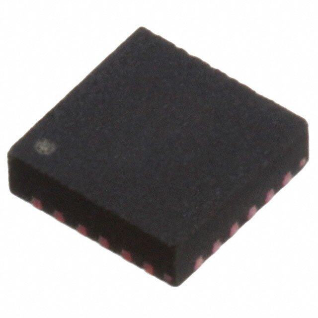
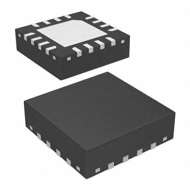
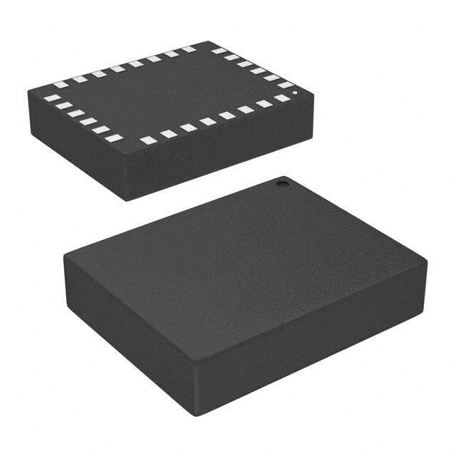
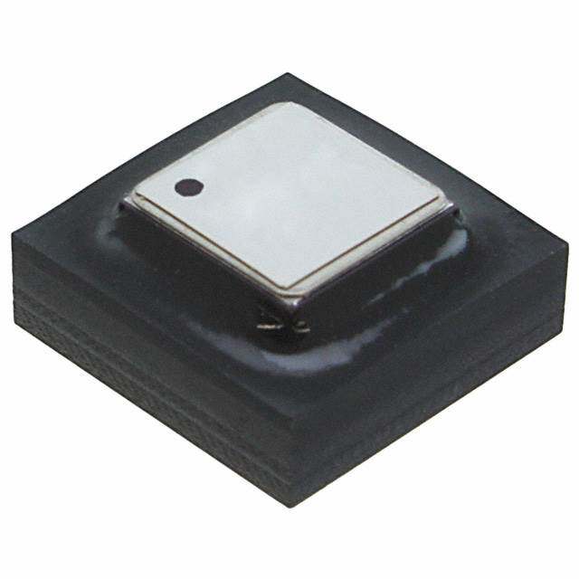
ICGOO在线商城 > 传感器,变送器 > 运动传感器 - 陀螺仪 > ADIS16136AMLZ
- 型号: ADIS16136AMLZ
- 制造商: Analog
- 库位|库存: xxxx|xxxx
- 要求:
| 数量阶梯 | 香港交货 | 国内含税 |
| +xxxx | $xxxx | ¥xxxx |
查看当月历史价格
查看今年历史价格
ADIS16136AMLZ产品简介:
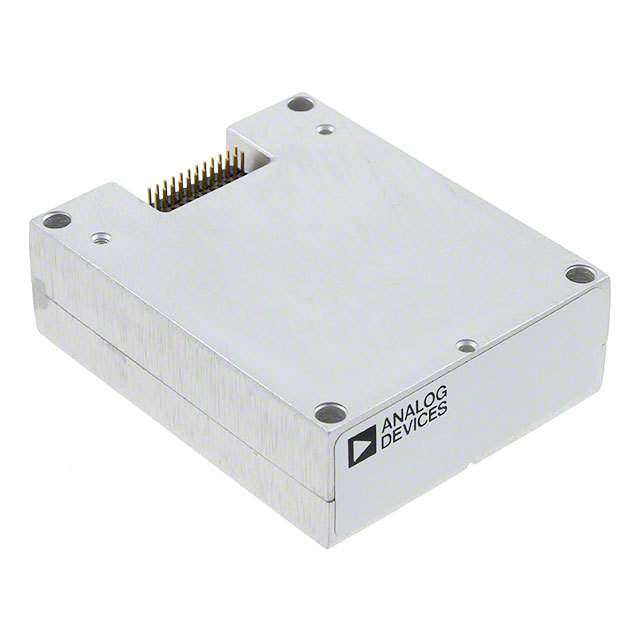
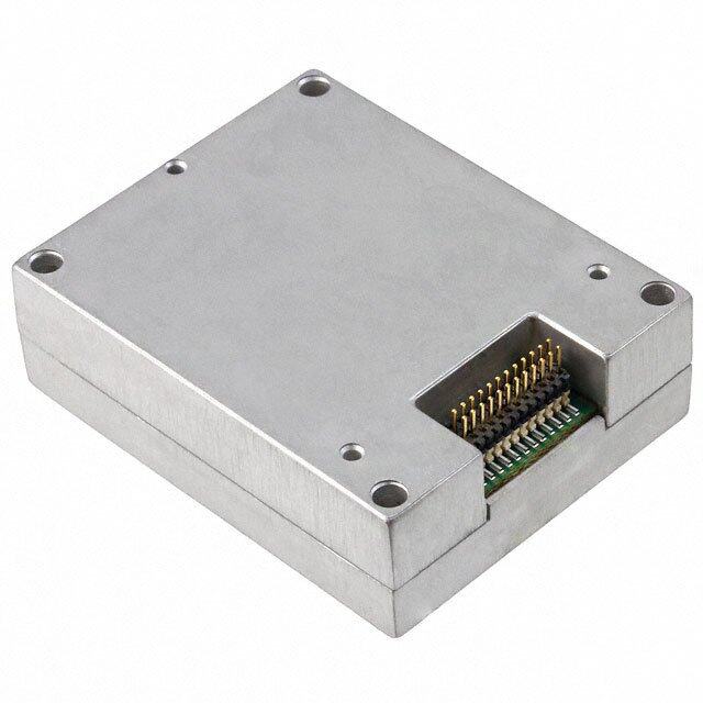
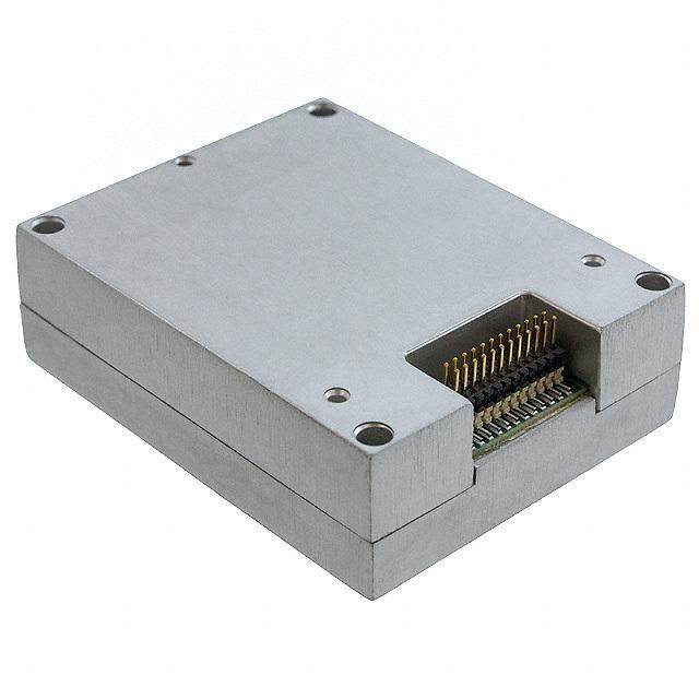
ICGOO电子元器件商城为您提供ADIS16136AMLZ由Analog设计生产,在icgoo商城现货销售,并且可以通过原厂、代理商等渠道进行代购。 ADIS16136AMLZ价格参考。AnalogADIS16136AMLZ封装/规格:运动传感器 - 陀螺仪, Gyroscope Z (Yaw) ±450 380Hz SPI Module。您可以下载ADIS16136AMLZ参考资料、Datasheet数据手册功能说明书,资料中有ADIS16136AMLZ 详细功能的应用电路图电压和使用方法及教程。
| 参数 | 数值 |
| 产品目录 | |
| 描述 | GYROSCOPE DIGITAL 24MSM螺旋仪 IC +/-450o/Sec Prec Angular Rate Sensor |
| 产品分类 | 陀螺仪运动与定位传感器 |
| 品牌 | Analog Devices |
| 产品手册 | |
| 产品图片 |
|
| rohs | RoHS 合规性豁免无铅 / 符合限制有害物质指令(RoHS)规范要求 |
| 产品系列 | 螺旋仪,Analog Devices ADIS16136AMLZ* |
| 数据手册 | |
| 产品型号 | ADIS16136AMLZ |
| 产品种类 | 螺旋仪 |
| 传感轴 | Z |
| 加速 | 2000 g |
| 商标 | Analog Devices |
| 宽度 | 44 mm |
| 封装 | Bulk |
| 封装/箱体 | Module-24 |
| 工厂包装数量 | 1 |
| 带宽 | 380 Hz |
| 数字输出-位数 | 16 bit |
| 数字输出-总线接口 | SPI |
| 最大工作温度 | + 85 C |
| 最小工作温度 | - 40 C |
| 标准包装 | 1 |
| 灵敏度 | 0.07139 deg/s/LSB |
| 电源电压-最大 | 5.25 V |
| 电源电压-最小 | 4.75 V |
| 电源电流 | 120 mA |
| 系列 | ADIS16136 |
| 范围 | +/- 450 deg/s |
| 输出类型 | Digital |
| 长度 | 36 mm |
| 高度 | 14 mm |



- 商务部:美国ITC正式对集成电路等产品启动337调查
- 曝三星4nm工艺存在良率问题 高通将骁龙8 Gen1或转产台积电
- 太阳诱电将投资9.5亿元在常州建新厂生产MLCC 预计2023年完工
- 英特尔发布欧洲新工厂建设计划 深化IDM 2.0 战略
- 台积电先进制程称霸业界 有大客户加持明年业绩稳了
- 达到5530亿美元!SIA预计今年全球半导体销售额将创下新高
- 英特尔拟将自动驾驶子公司Mobileye上市 估值或超500亿美元
- 三星加码芯片和SET,合并消费电子和移动部门,撤换高东真等 CEO
- 三星电子宣布重大人事变动 还合并消费电子和移动部门
- 海关总署:前11个月进口集成电路产品价值2.52万亿元 增长14.8%



PDF Datasheet 数据手册内容提取
±450°/Sec Precision Angular Rate Sensor Data Sheet ADIS16136 FEATURES GENERAL DESCRIPTION Digital gyroscope system, ±450°/sec measurement range The ADIS16136 iSensor® is a high performance, digital gyroscope In-run bias stability, 4°/hour sensing system that operates autonomously and requires no Autonomous operation and data collection user configuration to produce accurate rate sensing data. It No external configuration commands required provides performance advantages with its low noise density, Start-up time: 180 ms; sleep mode recovery: 2.5 ms wide bandwidth, and excellent in-run bias stability, which enable Factory calibrated sensitivity and bias applications such as platform control, navigation, robotics, and Calibration temperature range: −40°C to +70°C medical instrumentation. SPI-compatible serial interface This sensor system combines industry leading iMEMS® technology Wide bandwidth: 380 Hz with signal conditioning that optimizes dynamic performance. The Embedded temperature sensor factory calibration characterizes the entire sensor signal chain for Programmable operation and control sensitivity and bias over a temperature range of −40°C to +70°C. As Automatic and manual bias correction controls a result, each ADIS16136 has its own unique correction formulas Digital filters: Bartlett FIR, average/decimation to produce accurate measurements upon installation. For some Internal sample rate: up to 2048 SPS systems, the factory calibration eliminates the need for system Digital I/O: data ready, alarm indicator, general-purpose level calibration and greatly simplifies it for others. Alarms for condition monitoring Sleep mode for power management The ADIS16136 provides data at rates of up to 2048 SPS and Enable input sync operation offers an averaging/decimation filter structure for optimizing Single-supply operation: 4.75 V to 5.25 V noise/bandwidth trade-offs. The serial peripheral interface (SPI) 2000 g shock survivability and user register structure provide easy access to configuration Operating temperature range: −40°C to +85°C controls and calibrated sensor data for embedded processor platforms. APPLICATIONS The 36 mm × 44 mm × 14 mm package provides four holes for Precision instrumentation simple mechanical attachment, using M2 (or 2-56 standard size) Platform stabilization and control machine screws along with a standard 24-pin, dual row, 1 mm Industrial vehicle navigation pitch connector that supports electrical attachment to a printed Downhole instrumentation circuit board (PCB) or cable system. Robotics FUNCTIONAL BLOCK DIAGRAM DIO1DIO2DIO3DIO4/CLKIN RST VDD SELF-TEST I/O ALARMS POWER GND MANAGEMENT MEMS SENSOR USER CONTROLLER CONTROL REGISTERS CS TEMP SENSOR SCLK SPI CLOCK CALIBRATION PORT DIN OUTPUT DATA DOUT REGISTERS ADIS16136 FILTER 10249-001 Figure 1. Rev. D Document Feedback Information furnished by Analog Devices is believed to be accurate and reliable. However, no responsibility is assumed by Analog Devices for its use, nor for any infringements of patents or other One Technology Way, P.O. Box 9106, Norwood, MA 02062-9106, U.S.A. rights of third parties that may result from its use. Specifications subject to change without notice. No license is granted by implication or otherwise under any patent or patent rights of Analog Devices. Tel: 781.329.4700 ©2011–2014 Analog Devices, Inc. All rights reserved. Trademarks and registered trademarks are the property of their respective owners. Technical Support www.analog.com
ADIS16136 Data Sheet TABLE OF CONTENTS Features .............................................................................................. 1 Automatic Bias Correction (Autonull) .................................... 13 Applications ....................................................................................... 1 Manual Bias Correction ............................................................ 13 General Description ......................................................................... 1 Alarms .............................................................................................. 14 Functional Block Diagram .............................................................. 1 Static Alarm Use ......................................................................... 14 Revision History ............................................................................... 2 Dynamic Alarm Use .................................................................. 14 Specifications ..................................................................................... 3 Alarm Reporting ........................................................................ 14 Timing Specifications .................................................................. 4 System Controls .............................................................................. 15 Absolute Maximum Ratings ....................................................... 5 Global Commands ..................................................................... 15 ESD Caution .................................................................................. 5 Memory Management ............................................................... 15 Pin Configuration and Function Descriptions ............................. 6 General-Purpose Input/Output................................................ 15 Typical Performance Characteristics ............................................. 7 Automatic Self Test ..................................................................... 16 Theory of Operation ........................................................................ 8 Power Management.................................................................... 16 Reading Sensor Data .................................................................... 8 Status ............................................................................................ 16 Output Data Registers .................................................................. 9 Product Identification ................................................................ 17 Device Configuration .................................................................. 9 Applications Information .............................................................. 18 User Registers .................................................................................. 10 Power Supply Considerations ................................................... 18 Digital Processing Configuration ................................................. 11 Prototype Interface Board ......................................................... 18 Internal Sample Rate .................................................................. 11 Installation Tips .......................................................................... 19 Input Clock Configuration ........................................................ 11 Packaging and Ordering Information ......................................... 20 Digital Filtering ........................................................................... 11 Outline Dimensions ................................................................... 20 Averaging/Decimation Filter .................................................... 12 Ordering Guide .......................................................................... 20 Calibration ....................................................................................... 13 REVISION HISTORY 2/14—Rev. C to Rev. D Changes to Features Section............................................................ 1 Changes to Table 1 ............................................................................ 3 Changes to Table 5 ............................................................................ 6 9/13—Rev. B to Rev. C Changes to Prototype Interface Board Section, Figure 22, and Figure 23 ................................................................................... 18 2/13—Rev. A to Rev. B Changes to Table 1 ............................................................................ 3 Changes to Table 4 ............................................................................ 5 Changes to Table 31 and Automatic Self Test Section ............... 16 11/11—Rev. 0 to Rev. A Changes to Functional Times Parameters, Table 1 ...................... 3 10/11—Revision 0: Initial Version Rev. D | Page 2 of 20
Data Sheet ADIS16136 SPECIFICATIONS T = 25°C, VDD = 5.0 V, angular rate = 0°/sec, dynamic range = ±450°/sec, ±1 g, unless otherwise noted. A Table 1. Parameter Test Conditions/Comments Min Typ Max Unit GYROSCOPES Dynamic Range ±450 ±480 °/sec Sensitivity GYRO_OUT, GYRO_OUT2 (24 bits) 7.139x10⁻⁵ °/sec/LSB Repeatability1 −40°C ≤ T ≤ +70°C ±1 % A Sensitivity Temperature Coefficient −40°C ≤ T ≤ +70°C, 1 σ ±35 ppm/°C A Nonlinearity Best fit straight line, ±400°/sec ±0.01 % of FS Bias Repeatability1, 2 −40°C ≤ T ≤ +70°C, 1 σ ±0.15 °/sec A Bias Temperature Coefficient −40°C ≤ T ≤ +70°C, 1 σ ±0.00125 °/sec/°C A In-Run Bias Stability 25°C, SMPL_PRD = 0x000F 4 °/hr Angular Random Walk 1 σ, 25°C 0.167 °/√hr Linear Acceleration Effect on Bias 1 σ 0.017 °/sec/g Bias Voltage Sensitivity VDD = 4.75 V to 5.25 V, 1 σ ±0.08 °/sec/V Misalignment Axis-to-frame (package) ±1.0 Degrees Output Noise No filtering 0.11 °/sec rms Rate Noise Density f = 25 Hz, no filtering 0.00357 °/sec/√Hz rms 3 dB Bandwidth 380 Hz Sensor Resonant Frequency 15.5 17.5 20 kHz LOGIC INPUTS3 Input High Voltage, V 2.0 V IH Input Low Voltage, V 0.8 V IL Logic 1 Input Current, I V = 3.3 V ±0.2 ±1 µA IH IH Logic 0 Input Current, I V = 0 V IL IL All Pins Except RST 40 60 μA RST Pin 80 μA Input Capacitance, C 10 pF IN DIGITAL OUTPUTS3 Output High Voltage, V I = 1.6 mA 2.4 V OH SOURCE Output Low Voltage, V I = 1.6 mA 0.4 V OL SINK FLASH MEMORY Endurance4 10,000 Cycles Data Retention4 T = 85°C 20 Years J FUNCTIONAL TIMES5 Time until data is available Power-On Start-Up Time 245 ms Reset Recovery Time 128 ms Sleep Mode Recovery Time 2.5 ms Flash Memory Update 72 ms Flash Memory Self Test 21 ms Automatic Sensor Self Test Time SMPL_PRD ≠ 0x0000 245 ms SAMPLE RATE 6806 2048 SPS Internal Sample Rate Accuracy SMPL_PRD = 0x000F ±3 % Input Sync Clock Range SMPL_PRD = 0x0000 6806 2048 Hz POWER SUPPLY Operating voltage range, VDD 4.75 5.0 5.25 V Power Supply Current SMPL_PRD = 0x001F 120 mA Sleep mode 1.4 mA 1 The Repeatability specifications represent analytical projections, which are based off of the following drift contributions and conditions: temperature hysteresis (−40°C to +70°C), electronics drift (High-Temperature Operating Life test: +85°C, 500 hours), drift from temperature cycling (JESD22, Method A104-C, Method N, 500 cycles, −40°C to +85°C), rate random walk (10 year projection), and broadband noise 2 Bias repeatability describes a long-term behavior, over a variety of conditions. Short-term repeatability is related to the in-run bias stability and noise density specifications. 3 The digital I/O signals are driven by an internal 3.3 V supply, and the inputs are 5 V tolerant. 4 JEDEC Standard 22, Method A117. Endurance measured at −40°C, +25°C, +85°C, and +125°C. 5 These times do not include thermal settling and internal filter response times, which may affect overall accuracy. 6 The sync input clock and internal sampling clock function below the specified minimum value, at reduced performance levels. Rev. D | Page 3 of 20
ADIS16136 Data Sheet TIMING SPECIFICATIONS T = 25°C, VDD = 5 V, unless otherwise noted. A Table 2. Normal Mode Parameter Description Min1 Typ Max Unit f Serial clock 0.01 2.5 MHz SCLK t Stall period between data, see Figure 3 15 µs STALL t Read rate 25 µs READRATE t Chip select to clock edge 48.8 ns CS t DOUT valid after SCLK edge 25 ns DAV t DIN setup time before SCLK rising edge 24.4 ns DSU t DIN hold time after SCLK rising edge 48.8 ns DHD t , t SCLK rise and fall times 5 12.5 ns SCLKR SCLKF t , t DOUT rise and fall times 5 12.5 ns DR DF t CS high after SCLK edge 0 ns SFS t Input sync positive pulse width 5 µs 1 t Input sync to data ready output 300 µs 2 t Input sync period 488 µs 3 t Input sync low time 100 µs x 1 Guaranteed by design and characterization but not tested in production. Timing Diagrams CS tCS tSFS 1 2 3 4 5 6 15 16 SCLK tDAV DOUT MSB DB14 DB13 DB12 DB11 DB10 DB2 DB1 LSB tDSU tDHD DIN R/W A6 A5 A4 A3 A2 D2 D1 LSB 10249-002 Figure 2. SPI Timing and Sequence tREADRATE tSTALL CS SCLK 10249-003 Figure 3. Stall Time and Data Rate t3 t2 t1 tX SYNC CLOCK (CLKIN) REDAADTAY 10249-004 Figure 4. Input Clock Timing Diagram Rev. D | Page 4 of 20
Data Sheet ADIS16136 ABSOLUTE MAXIMUM RATINGS Table 3. Stresses abovethose listedunderAbsoluteMaximumRatings Parameter Rating may causepermanentdamagetothedevice.This is a stress Acceleration ratingonly;functionaloperationofthedeviceattheseorany Any Axis, Unpowered 2000 g otherconditionsabovethoseindicatedintheoperational Any Axis, Powered 2000 g sectionofthisspecificationisnotimplied.Exposuretoabsolute VDD to GND −0.3 V to +6.0 V maximumratingconditionsfor extendedperiodsmayaffect Digital Input Voltage to GND −0.3 V to +5.3 V devicereliability. Digital Output Voltage to GND −0.3 V to VDD + 0.3 V Operating Temperature Range −40°C to +85°C Table 4. Package Characteristics Storage Temperature Range −65°C to +125°C1, 2 Device Package Type θ θ Weight 1 Extended exposure to temperatures outside the specified temperature JA JC range of −40°C to +105°C can adversely affect the accuracy of the factory 24-Lead Module with Connector 15.7 1.48 31 g calibration. For best accuracy, store the devices within the specified Interface operating range of −40°C to +105°C. 2 Although the device is capable of withstanding short term exposure to 150°C, long-term exposure threatens internal mechanical integrity. ESD CAUTION Rev. D | Page 5 of 20
ADIS16136 Data Sheet PIN CONFIGURATION AND FUNCTION DESCRIPTIONS ADIS16136 TOP VIEW 24 22 20 18 16 14 12 10 8 6 4 2 23 21 19 17 15 13 11 9 7 5 3 1 NOTES 12..PSUIHSNOES WS AANRM ERT ENEPOCRT CE VSLIMESN-I1BT1L 2TE-H0 FE2R OMORAM TE TIQNHUGISI VC VAOILENEWNNE.T CT.HTOE RP IANS ASSIGSNIGMNEMNETNST.S 10249-005 Figure 5. Mating Connector Pin Assignments RATE AXIS POSITIVE ROTATION DIRECTION + 10249-006 Figure 6. Axial Orientation (Bottom Side Facing Up) Table 5. Pin Function Descriptions Pin No. Mnemonic Type1 Description 1 DIO3 I/O Configurable Digital Input/Output. 2 DIO4/CLKIN I Configurable Digital Input/Output/Clock Input 3 SCLK I SPI Serial Clock. 4 DOUT O SPI Data Output. Clocks output on SCLK falling edge. 5 DIN I SPI Data Input. Clocks input on SCLK rising edge. 6 CS I SPI Chip Select. 7 DIO1 I/O Configurable Digital Input/Output. 8 RST I Reset. 9 DIO2 I/O Configurable Digital Input/Output. 10, 11, 12 VDD S Power Supply. 13, 14, 15 GND S Power Ground. 16 to 24 DNC N/A Do Not Connect. Do not connect to these pins. 1 I/O is input/output, I is input, O is output, S is supply, N/A is not applicable. Rev. D | Page 6 of 20
Data Sheet ADIS16136 TYPICAL PERFORMANCE CHARACTERISTICS 100 0.20 +1σ INITIAL BIAS ERROR = ±0.1° AVERAGE BIAS TEMPERATURE COEFFICIENT = ±0.00125°/sec/°C –1σ 0.15 ANCE (°/Hr) R (°/sec)00..0150 RI O VA 10 RR 0 AN T E LL SE–0.05 A F OT OF O –0.10 R –0.15 10.01 0.1 1 TAU (S1e0conds) 100 1000 10000 10249-025 –0.20–40 –30 –20 –10 0TEMP1E0RAT20URE3 (0°C)40 50 60 70 10249-027 Figure 7. Root Allan Variance, 5 V, 25°C, 1024 SPS Figure 9. Offset (Bias) Error vs. Temperature, −40°C to +75°C to −40°C 0.60 0.40 %) INITIAL SENSITIVITY ERROR = ±0.35% R ( 0.20 SENSITIVITIY TEMPC = ±25ppm/°C O R R E Y 0 T VI TI SI N–0.20 E S –0.40 –0.60–45 –35 –25 –15 –5TEM5PER1A5TU2R5E (°3C5) 45 55 65 75 10249-026 Figure 8. Sensitivity Error vs. Temperature, −40°C to +75°C to −40°C Rev. D | Page 7 of 20
ADIS16136 Data Sheet THEORY OF OPERATION The ADIS16136 is an autonomous system that requires no user Table 7. Generic Master Processor SPI Settings initialization. As soon as it has a valid power supply, it initializes Processor Setting Description and starts sampling, processing, and loading sensor data into Master ADIS16136 operates as a slave the output registers. After each sample cycle concludes, DIO1 SCLK Rate ≤ 2 MHz Maximum serial clock rate pulses high. The SPI interface enables simple integration with SPI Mode 3 CPOL = 1 (polarity), CPHA = 1 (phase) many embedded processor platforms, as shown in Figure 10 MSB First Mode Bit sequence (electrical connection) and Table 6 (processor pin names and 16-Bit Mode Shift register/data length functions). READING SENSOR DATA I/O LINES ARE COMPATIBLE WITH 5V 3.3V OR 5V LOGIC LEVELS VDD A single register read requires two 16-bit SPI cycles. The first 10 11 12 cycle requests the contents of a register using the bit assignments SPYRSOTCEEMSSOR SS 6 CS ADIS16136 in Figure 13. Then, the register contents follow on DOUT during SPI MASTER the second sequence. Figure 11 includes three single register reads SCLK 3 SCLK in succession. In this example, the process starts with Pin 5, MOSI 5 DIN DIN = 0x0600, to request the contents of the GYRO_OUT MISO 4 DOUT register and follows with 0x0400 to request the contents of the IRQ 7 DIO1 GYRO_OUT2 register and with 0x0200 to request the contents 13 14 15 10249-010 ocef stshoer sT tEoM uPse_ tOheU sTam reeg 1is6t-ebri.t F SuPlIl cdyucplele txo orepaedr adtaiotan f reonmab DleOs pUrTo - Figure 10. Electrical Connection Diagram while requesting the next set of data on the DIN pin. Figure 12 provides an example of the four SPI signals when reading Table 6. Generic Master Processor Pin Names and Functions GYRO_OUT in a repeating pattern. Pin Name Function SS Slave select DIN 0x0600 0x0400 0x0200 IMRQO SI IMntaesrtreurp otu rtepquute, sslta ve input DOUT GYRO_OUT GYRO_OUT2 TEMP_OUT 10249-011 MISO Master input, slave output Figure 11. SPI Read Example SCLK Serial clock CS The ADIS16136 SPI interface supports full duplex serial SCLK communication (simultaneous transmit and receive) and uses DIN DIN = 0000 0110 0000 0000 = 0x0600 the bit sequence shown in Figure 13. Table 7 provides a list of tphreo cmesossotr c soemrimal opno rste tftoirn gths et hAaDt rIeSq1u6i1r3e6 a SttPeIn tiniotner tfoa cien.i tialize a DDOOUUTT = 1111 1001 1101 1010 = 0xF9DA = –1574 LSBs = –29.765°/sec 10249-012 Figure 12. SPI Read Example, Second 16-Bit Sequence CS SCLK DIN R/W A6 A5 A4 A3 A2 A1 A0 DC7 DC6 DC5 DC4 DC3 DC2 DC1 DC0 R/W A6 A5 DOUT D15 D14 D13 D12 D11 D10 D9 D8 D7 D6 D5 D4 D3 D2 D1 D0 D15 D14 D13 NOTES 12..DWFOOHRUE TNO BTCIHSTE SIRS A DHREIEGV HPICR, EDOSOD.UUTC EISD I NO NAL TYH WREHEE-NS TTAHTEE P, RHEIGVHIO-IUMSP 1E6D-ABNITC DEI NM OSEDQEU, WENHCICEH S ATLALROTWS SW MITUHL RT/IWFU =N 0C.TIONAL USE OF THE LINE 10249-013 Figure 13. SPI Communication Bit Sequence Rev. D | Page 8 of 20
Data Sheet ADIS16136 OUTPUT DATA REGISTERS Table 12. TEMP_OUT Bit Descriptions Bits Description Table 8. Output Data Register Formats [15:0] Temperature data; twos complement, 0.010697°C per Register Address Measurement LSB, 0°C = 0x0000 TEMP_OUT 0x02 Internal temperature GYRO_OUT2 0x04 Gyroscope, lower 16 bits Table 13. Temperature, Twos Complement Format GYRO_OUT 0x06 Gyroscope, upper 16 bits Temperature Decimal Hex Binary Rotation Rate (Gyroscope) +85°C +7946 0x1F0A 0001 1111 0000 1010 +0.021394°C +2 0x0002 0000 0000 0000 0010 GYRO_OUT is the primary register for gyroscope output data +0.010697°C +1 0x0001 0000 0000 0000 0001 and uses 16-bit twos complement format for its data. Table 9 0°C 0 0x0000 0000 0000 0000 0000 provides the numerical format, and Table 10 provides several −0.010697 °C −1 0xFFFF 1111 1111 1111 1111 examples for converting digital data into °/sec. −0.021394°C −2 0xFFFE 1111 1111 1111 1110 Table 9. GYRO_OUT Bit Descriptions −40°C −3739 0xF165 1111 0001 0110 0101 Bits Description DEVICE CONFIGURATION [15:0] Gyroscope data; twos complement, 0.018275°/sec per LSB, 0°/sec = 0x0000 The control registers listed in Table 14 provide a variety of user configuration options. The SPI provides access to these registers, Table 10. GYRO_OUT, Twos Complement Format one byte at a time, using the bit assignments shown in Figure 13. Rotation Rate Decimal Hex Binary Each register has 16 bits, wherein Bits[7:0] represent the lower +450°/sec +24,623 0x602F 0110 0000 0010 1111 address and Bits[15:8] represent the upper address. +0.03655°/sec +2 0x0002 0000 0000 0000 0010 Figure 15 provides an example of writing 0x03 to Address 0x22 +0.018275°/sec +1 0x0001 0000 0000 0000 0001 (DEC_RATE[7:0]), using Pin 5, DIN = 0xA203. This example 0°/sec 0 0x0000 0000 0000 0000 0000 reduces the sample rate by a factor of 8 (see Table 16). −0.018275°/sec −1 0xFFFF 1111 1111 1111 1111 −0.03655°/sec −2 0xFFFE 1111 1111 1111 1110 CS −450°/sec −24,623 0x9FD1 1001 1111 1101 0001 SCLK Tashseo cGiaYteRdO w_iOthU tTh2e rdeegciismteart i(osene a Tnadb FleI R11 f)i lcteaprst uthreast tahree bsiht ogwronw itnh DIND I=N 1010 0010 0000 0011 = 0xA203, WRITES 0x03 TO ADDRESS 0x22 10249-015 Figure 18 using a MSB justified format. The bit growth starts Figure 15. SPI Sequence for Setting the Decimate Rate to 8 (DIN = 0xA203) with the MSB (GYRO_OUT2[15]), is equal to the decimation Dual Memory Structure rate setting in DEC_RATE[4:0] (see Table 18), and grows in the Writing configuration data to a control register updates its SRAM LSB direction as the decimation rate increases. See Figure 14 for contents, which are volatile. After optimizing each relevant control more details. register setting in a system, set GLOB_CMD[3] = 1 (DIN = Table 11. GYRO_OUT2 Bit Descriptions 0xA808) to backup these settings in the nonvolatile flash memory. Bits Description The flash back up process requires a valid power supply level for [15:0] Rotation rate data; resolution enhancement bits the entire 72 ms process time. Table 14 provides a user register memory map that includes a column of flash backup information. A “yes” in this column indicates that a register has a mirror location D D = DEC_RATE[4:0] in flash and, when backed up properly, automatically restores itself during startup or after a reset. Figure 16 provides a diagram of the GYROSCOPE DATA NOT USED dual memory structure that is used to manage operation and store 15 GYRO_OUT 015 GYRO_OUT2 0 critical user settings. BIT WEIGHT =0.0128D275 °L/sSeBcLSB = GYRO_OUT2[16-D] 10249-014 MANUAL Figure 14. Gyroscope Output Format, DEC_RATE[4:0] > 0 FLASH BACKUP Internal Temperature NONVOLATILE VOLATILE FLASH MEMORY SRAM The TEMP_OUT register (see Table 12) provides an internal (NO SPI ACCESS) SPI ACCESS temperature measurement that can be useful for observing START-UP rperloavtiivdee st esmevpeerraalt cuorde icnhga enxgaems ipnl etsh feo ern cvoinrovnermtienngt .t hTea b1l6e- 1b3it RESET 10249-016 twos complement number into units for temperature (°C). Figure 16. SRAM and Flash Memory Diagram Rev. D | Page 9 of 20
ADIS16136 Data Sheet USER REGISTERS Table 14. User Register Memory Map Name R/W Flash Backup Address1 Default Register Description Bit Descriptions FLASH_CNT R Yes 0x00 N/A2 Flash memory write count Table 30 TEMP_OUT R No 0x02 N/A2 Output, temperature (internal) Table 12 GYRO_OUT2 R No 0x04 N/A2 Output, gyroscope, lower 16 bits Table 11 GYRO_OUT R No 0x06 N/A2 Output, gyroscope, upper 16 bits Table 9 GYRO_OFF2 R/W Yes 0x08 0x0000 Gyroscope bias correction, lower 16 bits Table 21 GYRO_OFF R/W Yes 0x0A 0x0000 Gyroscope bias correction, upper 16 bits Table 20 Reserved N/A2 N/A2 0x0C to 0x0F N/A2 Reserved ALM_MAG1 R/W Yes 0x10 0x0000 Alarm 1 trigger setting Table 23 ALM_MAG2 R/W Yes 0x12 0x0000 Alarm 2 trigger setting Table 24 ALM_SMPL1 R/W Yes 0x14 0x0000 Alarm 1 sample period Table 25 ALM_SMPL2 R/W Yes 0x16 0x0000 Alarm 2 sample period Table 25 ALM_CTRL R/W Yes 0x18 0x0000 Alarm configuration Table 26 GPIO_CTRL R/W Yes 0x1A 0x0000 Auxiliary digital input/output control Table 32 MSC_CTRL R/W Yes 0x1C 0x0006 Miscellaneous control: data ready, self test Table 31 SMPL_PRD R/W Yes 0x1E 0x001F Internal sample period (rate) control Table 16 AVG_CNT R/W Yes 0x20 0x0000 Digital filter control Table 17 DEC_RATE R/W Yes 0x22 0x0000 Decimation rate setting Table 18 SLP_CTRL W Yes 0x24 0x0000 Sleep mode control Table 33 DIAG_STAT R No 0x26 0x0000 System status Table 34 GLOB_CMD W No 0x28 0x0000 System command Table 29 Reserved N/A2 N/A2 0x2A to 0x31 N/A2 Reserved LOT_ID1 R Yes 0x32 N/A2 Lot Identification Code 1 Table 36 LOT_ID2 R Yes 0x34 N/A2 Lot Identification Code 2 Table 36 LOT_ID3 R Yes 0x36 N/A2 Lot Identification Code 3 Table 36 PROD_ID R Yes 0x38 0x3F08 Product ID, binary number for 16,136 Table 35 SERIAL_NUM R Yes 0x3A N/A2 Serial number Table 37 1 Each register contains two bytes. The address column in this table only offers the address of the lower byte. Add 1 to it to calculate the address of the upper byte. 2 N/A means not applicable. Rev. D | Page 10 of 20
Data Sheet ADIS16136 DIGITAL PROCESSING CONFIGURATION Figure 18 provides a block diagram for the sampling and digital INPUT CLOCK CONFIGURATION filter stages inside the ADIS16136. Table 15 provides a summary Set SMPL_PRD = 0x0000 (DIN = 0x9F00, then DIN = 0x9E00) of registers for sample rate and filter control. to disable the internal clock and enable DIO4/CLKIN as a clock Table 15. Digital Processing Registers input pin. Register Name Address Description DIGITAL FILTERING SMPL_PRD 0x1E Sample rate control The AVG_CNT register (see Table 17) provides user controls AVG_CNT 0x20 Digital filtering and range control for the low-pass filter. This filter contains two cascaded averaging DEC_RATE 0x22 Decimation rate setting filters that provide a Bartlett window FIR filter response (see INTERNAL SAMPLE RATE Figure 18). For example, set AVG_CNT[7:0] = 0x04 (DIN = The SMPL_PRD register in Table 16 provides a programmable 0xA004) to set each stage to 16 taps. When used with the default control for the internal sample rate. Use the following formula sample rate of 1024 SPS, this establishes a −3 dB bandwidth of to calculate the decimal number for the code to write into this approximately 24 Hz for this filter. register: 0 32,768 SMPL_PRD= (f ) −1; fS ≤ 2048 SPS –20 S –40 The factory default setting for SMPL_PRD sets the internal B) d sample rate to a rate of 1024 SPS; the minimum setting for the E ( –60 D SMPL_PRD register is 0x000F, which results in an internal TU sample rate of 2048 SPS. GNI –80 A M Table 16. SMPL_PRD Bit Descriptions –100 Bits Description (Default = 0x001F) N = 2 –120 N = 4 [15:0] Clock setting bits; sets f in Figure 18 N = 16 S N = 64 –140 0.001 0.01FREQUENCY (f/fS)0.1 1 10249-017 Figure 17. Bartlett Window FIR Filter Frequency Response Table 17. AVG_CNT Bit Descriptions Bits Description (Default = 0x0000) [15:3] Don’t care [2:0] Binary; B variable in Figure 18; maximum = 110 (6) Rev. D | Page 11 of 20
ADIS16136 Data Sheet AVERAGING/DECIMATION FILTER When the factory default 1024 SPS sample rate is used, this decimation setting reduces the output data rate to 64 SPS and The DEC_RATE register (see Table 18) provides user control the sensor bandwidth to approximately 32 Hz. for the final filter stage (see Figure 18), which averages and decimates the output data. For systems that value lower sample Table 18. DEC_RATE Bit Descriptions rates, this filter stage provides an opportunity to lower the sample Bits Description (Default = 0x0000) rate while maintaining optimal bias stability performance. The [15:5] Don’t care −3 dB bandwidth of this filter stage is approximately one half [4:0] Binary; D variable in Figure 18; maximum = 10000 (16) the output data rate. For example, set DEC_RATE[7:0] = 0x04 (DIN = 0xA204) to reduce the sample rate by a factor of 16. MEMS ÷ND GYRO 410Hz 1595Hz –3dB BANDWIDTH = 380Hz CLOCK fSSSPP = ≥= 3S1S25PM, 7P+6 L81_PRD CLfKSIN BNNN TBT= = ==A 22TVNBOGBT_ A–C LN1 TN[U2:M0]BER OF TAPS DNNN DDD= ===D 2NDEDUACMT_RABA ERTRAE TO[4EF: 0 DT]IAVPISSOR 10249-018 Figure 18. Sampling and Frequency Response Block Diagram Rev. D | Page 12 of 20
Data Sheet ADIS16136 CALIBRATION The Allan variance curve shown in Figure 7 provides a trade-off The ADIS16136 factory calibration produces correction between bias accuracy and averaging time. The DEC_RATE formulas for the gyroscope and programs them into the flash register provides a user control for averaging time when using memory. Table 19 contains a list of user control registers that the ABC function. Set DEC_RATE[7:0] = 0x10 (DIN = 0xA210), provide an opportunity for user optimization after installation. which sets the decimation rate to 65,536 (216) and provides an Figure 19 illustrates the summing function of the sensor’s offset averaging time of 64 seconds (65,536 ÷ 1024 SPS) for this function. correction register. Next, set GLOB_CMD[0] = 1 (DIN = 0xA801), and keep the Table 19. Registers for User Calibration platform stable for at least 65 seconds while the gyroscope bias Register Address Description data accumulates. GYRO_OFF2 0x08 Gyroscope bias After this completes, the ADIS16136 automatically updates the GYRO_OFF 0x0A Gyroscope bias flash memory. When the ABC function starts, the SPI is not active. GLOB_CMD 0x28 Bias correction command The only way to interrupt the ABC function is to remove power or initiate a hardware reset using the RST pin. When using FACTORY DEC_RATE = 0x0010, the 1 σ accuracy for this correction is MGYERMOS ADC CALIBARNADTION GYRO_OUT GYRO_OUT2 approximately 0.001°/sec for the gyroscope correction factor. FILTERING GYRO_OFF GYRO_OFF2 10249-019 SMeeA TNabUleA 2L9 BfoIrA mSo CreO iRnfRorEmCaTtiIoOnN o n GLOB_CMD. Figure 19. Gyroscope Bias Calibration User Controls The GYRO_OFF and GYRO_OFF2 registers (see Table 20 and The factory calibration addresses initial and temperature Table 21) provide a bias adjustment function for the output of dependent bias errors in the gyroscopes, but some environ- each sensor. GYRO_OFF has the same format as GYRO_OUT, mental conditions, such as temperature cycling and mechanical and GYRO_OFF2 has the same format as GYRO_OUT2. stress on the package, can cause bias shifts in MEMS gyroscope Table 20. GYRO_OFF Bit Descriptions structures. For systems that value absolute bias accuracy, there Bits Description (Default = 0x0000) are two options for optimizing absolute bias accuracy: autonull [15:0] Gyroscope offset correction; twos complement, and manual correction. 0.018275°/sec per LSB AUTOMATIC BIAS CORRECTION (AUTONULL) Table 21. GYRO_OFF2 Bit Descriptions Set GLOB_CMD[0] = 1 (DIN = 0xA801) to start the automatic Bits Description (Default = 0x0000) bias correction (ABC) function, which uses the following [15:0] Gyroscope offset correction, finer resolution; uses internal sequence to calibrate each gyroscope for bias error: same format as GYRO_OUT2 (see Table 11) 1. Wait for a complete output data cycle to complete, which Restoring Factory Calibration includes the entire average and decimation time in DEC_RATE. Set GLOB_CMD[1] = 1 (DIN = 0xA802) to execute the factory 2. Read the output registers of the gyroscope. calibration restore function. This function resets each user 3. Multiply the measurement by −1 to change its polarity. calibration register to 0x0000, resets all sensor data to 0, and 4. Write the final value into the offset registers. automatically updates the flash memory within 72 ms. See 5. Update the flash memory. Table 29 for more information on GLOB_CMD. Rev. D | Page 13 of 20
ADIS16136 Data Sheet ALARMS The alarm function provides monitoring for two independent Table 26. ALM_CTRL Bit Descriptions conditions. Table 22 contains a list of registers that provide Bits Description (Default = 0x0000) configuration and control inputs for the alarm function. [15:12] Alarm 2 source selection 0000 = disable Table 22. Registers for Alarm Configuration 0001 = GYRO_OUT (does not include GYRO_OUT2) Register Address Description 0010 = TEMP_OUT ALM_MAG1 0x10 Alarm 1, trigger setting 0011 = DIAG_STAT ALM_MAG2 0x12 Alarm 2, trigger setting [11:8] Alarm 1 source selection (same as Alarm 2) ALM_SMPL1 0x14 Alarm 1, sample period 7 Rate-of-change enable for Alarm 2 ALM_SMPL2 0x16 Alarm 2, sample period (1 = rate of change, 0 = static level) ALM_CTRL 0x18 Alarm configuration 6 Rate-of-change enable for Alarm 1 The ALM_CTRL register (see Table 26) provides data source (1 = rate of change, 0 = static level) selection (Bits[15:8]), static/dynamic setting for each alarm 5 Comparison polarity for Alarm 2 (Bits[7:6]), trigger polarity (Bits[5:4]), data source filtering (1 specifies >ALM_MAG2, 0 specifies <ALM_MAG2) (Bit 3), and an alarm indicator signal (Bits[2:0]). 4 Comparison polarity for Alarm 1 STATIC ALARM USE (1 specifies >ALM_MAG1, 0 specifies <ALM_MAG1) 3 Comparison data filter setting1 The static alarms setting compares the data source selection (1 = Bartlett filter, 0 = no filtering) (ALM_CTRL[15:8]) with the values in the ALM_MAGx 2 Alarm output enable registers in Table 23 and Table 24. The data format in these (1 = enabled, 0 = disabled) registers matches the format of the data selection in 1 Alarm output polarity ALM_CTRL[15:8]. ALM_CTRL[5:4] provide polarity (1 = active high, 0 = active low) settings. See Table 27 for a static alarm configuration 0 Alarm output line select example. (1 = DIO2, 0 = DIO1) Table 23. ALM_MAG1 Bit Descriptions 1 Filtering applies to GYRO_OUT only. Bits Description (Default = 0x0000) Alarm Example [15:0] Threshold setting; matches format of the Table 27 offers an example that configures Alarm 1 to trigger ALM_CTRL[11:8] selection when filtered GYRO_OUT data drops below 50°/sec and Alarm 2 to trigger when filtered GYRO_OUT data changes by more Table 24. ALM_MAG2 Bit Descriptions than 50°/sec over a 100 ms period, or 500°/sec2. The filter Bits Description (Default = 0x0000) setting helps reduce false triggers from noise and refine the [15:0] Threshold setting; matches for format of the ALM_CTRL[15:12] selection accuracy of the trigger points. The ALM_SMPL2 setting of 102 samples provides a comparison period that is 99.6 ms for DYNAMIC ALARM USE an internal sample rate of 1024 SPS. There is no need to pro- The dynamic alarm setting monitors the data selection for a gram ALM_SMPL1 because Alarm 1 is a static alarm in this rate-of-change comparison. The rate of change is represented example. by the magnitude in the ALM_MAGx registers over the time Table 27. Alarm Configuration Example 1 represented by the number of samples in the ALM_SMPLx DIN Description register (see Table 25). See Table 27 for a dynamic alarm 0x9911, ALM_CTRL = 0x11AF configuration example. 0x98AF Alarm 2: dynamic; ΔGYRO_OUT Table 25. ALM_SMPL1, ALM_SMPL2 Bit Descriptions (Δtime, ALM_ SMPL2) > ALM_MAG2 Alarm 1: static; GYRO_OUT < ALM_MAG1 Bits Description (Default = 0x0000) use filtered data source for comparison [15:8] Not used DIO2 output indicator, positive polarity [7:0] Binary, number of samples (both 0x00 and 0x01 = 1) 0x930A, ALM_MAG2 = 0x0AAF, (+50°/sec) ALARM REPORTING 0x92AF 0x910A, ALM_MAG1 = 0x0AAF, (+50°/sec) DIAG_STAT[9:8] provide error flags that indicate an alarm 0x90AF condition. ALM_CTRL[2:0] provide controls for a hardware 0x9666 ALM_SMPL2[7:0] = 0x66, (102 samples) indicator using DIO1 or DIO2. Rev. D | Page 14 of 20
Data Sheet ADIS16136 SYSTEM CONTROLS The ADIS16136 provides a number of system level controls for managing its operation using the registers listed in Table 28. 600 Table 28. System Tool Registers Register Name Address Description s) ar450 GPIO_CTRL 0x1A General-purpose I/O control Ye N ( MSC_CTRL 0x1C Self test, calibration, data ready O TI SLP_CTRL 0x24 Sleep mode control EN300 T DIAG_STAT 0x26 Error flags E R GLOB_CMD 0x28 Single command functions 150 LOT_ID1 0x32 Lot Identification Code 1 LOT_ID2 0x34 Lot Identification Code 2 LPOROT_DID_I3D 00xx3386 LPorot dIduecnt tiidfiecnattiifoicna Ctioodne 3 0 30 40 55JUNCT7IO0N TEM85PERAT1U00RE (°C12)5 135 150 10249-113 SERIAL_NUM 0x3A Serial number Figure 20. Flash Memory Retention GLOBAL COMMANDS Checksum Test The GLOB_CMD register (see Table 29) provides trigger Set MSC_CTRL[11] = 1 (DIN = 0x9D08) to perform a checksum bits for several operations. Write 1 to the appropriate bit in verification of the internal program memory. This takes a summa- GLOB_CMD to start a function. After the function completes, tion of the internal program memory and compares it with the the bit restores to 0. original summation value for the same locations (from factory configuration). Check the results in the DIAG_STAT register Software Reset (see Table 34). DIAG_STAT[6] = 0 if the sum matches the Set GLOB_CMD[7] = 1 (DIN = 0xA880) to reset the operation, correct value and 1 if it does not. Make sure that the power which removes all data, initializes all registers from their flash supply is within specification for the entire 21 ms that this settings, and starts data collection. This function provides a function takes to complete. firmware alternative to the RST line (see Table 5, Pin 8). GENERAL-PURPOSE INPUT/OUTPUT Table 29. GLOB_CMD Bit Descriptions There are four general-purpose I/O lines, DIO1, DIO2, DIO3, Bits Description (Default = 0x0000) Execution Time1 and DIO4/CLKIN that provide a number of useful functions. The [15:8] Not used N/A MSC_CTRL[2:0] bits (see Table 31) control the data ready configu- 7 Software reset 70 ms ration and have the highest priority for setting either DIO1 or DIO2 [6:4] Not used N/A (but not both). The ALM_CTRL[2:0] control bits (see Table 26) 3 Flash update 70 ms provide the alarm indicator configuration control and have the 2 Not used N/A second highest priority for DIO1 or DIO2. When DIO1 and DIO2 1 Factory calibration restore 71 ms are not in use as either data ready or alarm indicator signals, the 0 Automatic bias correction N/A2 GPIO_CTRL register (see Table 32) provides the control and data 1 N/A in this column means not applicable. bits for them, together with the DIO3 and DIO4 lines. 2 Execution time is based on SMPL_PRD and DEC_RATE settings. This starts Data Ready Input/Output Indicator at the next data ready pulse, restarts the decimation cycle, and then writes to the flash (70 ms) after completing a decimation cycle. With respect to The factory default setting for MSC_CTRL[2:0] is 110, which Figure 18, the decimation cycle time = N ÷ f. D S configures DIO1 as a positive data ready indicator signal. A MEMORY MANAGEMENT common option for this function is MSC_CTRL[2:0] = 100 The data retention of the flash memory depends on the temper- (DIN = 0x9C04), which changes data ready to a negative ature, as shown in Figure 20. The FLASH_CNT register (see polarity for processors that provide only negative triggered Table 30) provides a 16-bit counter that helps track the number interrupt pins. The pulse width is between 100 μs and 200 μs of write cycles to the nonvolatile flash memory, which helps the over all conditions. user manage against the endurance rating. The flash updates Example Input/Output Configuration every time any of the following bits are set to 1: GLOB_CMD[3], For example, set GPIO_CTRL[7:0] = 0x02 (DIN = 0x9A02) GLOB_CMD[1], and GLOB_ CMD[0]. to set DIO1 as an input and DIO2 as an output. Then, set Table 30. FLASH_CNT Bit Descriptions GPIO_CTRL[15:8] = 0x02 (DIN = 0x9B02) to set DIO2 in a Bits Description) high output state. Monitor DIO1 by reading GPIO_CTRL[8] [15:0] Binary counter; number of flash updates (DIN = 0x1B00). Rev. D | Page 15 of 20
ADIS16136 Data Sheet Table 31. MSC_CTRL Bit Descriptions POWER MANAGEMENT Bits Description (Default = 0x0006) The SLP_CTRL register (see Table 33) provides two different [15:12] Not used sleep modes for system level management: normal and timed. 11 Memory test (cleared upon completion) Set SLP_CTRL[7:0] = 0xFF (DIN = 0xA4FF) to start normal (1 = enabled, 0 = disabled) sleep mode. To awaken the device from sleep mode, use one of 10 Automatic self test (cleared upon completion) the following options to restore normal operation: assert CS from (1 = enabled, 0 = disabled) high to low, pulse RST low, then high again, or cycle the power. Use [9:8] Do not use, always set both bits to zero. SLP_CTRL[7:0] to put the device into sleep mode for a specified 7 Disable sensor compensation period. For example, SLP_CTRL[7:0] = 0x64 (DIN = 0xA464) (1 = disable compensation, 0 = enable compensation) puts the ADIS16136 to sleep for 50 sec. [6:3] Not used 2 Data ready enable Table 33. SLP_CTRL Bit Descriptions (1 = enabled, 0 = disabled) Bits Description 1 Data ready polarity [15:8] Not used (1 = active high, 0 = active low) [7:0] 0xFF: normal sleep mode 0 Data ready line select 0x00 to 0xFE: programmable sleep time bits; 0.5 sec/LSB (1 = DIO2, 0 = DIO1) STATUS Table 32. GPIO_CTRL Bit Descriptions The DIAG_STAT register (see Table 34) provides error flags for Bits Description (Default = 0x0000) a number of functions. Each flag uses a 1 to indicate an error [15:12] Don’t care condition and a 0 to indicate a normal condition. Reading this register provides access to the status of each flag and resets all of 11 General-Purpose I/O Line 4 (DIO4) data level the bits to 0 for monitoring future operation. If the error 10 General-Purpose I/O Line 3 (DIO3) data level condition remains, the error flag returns to 1 at the conclusion 9 General-Purpose I/O Line 2 (DIO2) data level of the next sample cycle. The SPI communication error flag in 8 General-Purpose I/O Line 1 (DIO1) data level DIAG_STAT[3] indicates that the number of SCLKs in a SPI [7:4] Don’t care sequence did not equal a multiple of 16 SCLKs. 3 General-Purpose I/O Line 2 (DIO2) direction control (1 = output, 0 = input) Table 34. DIAG_STAT Bit Descriptions 2 General-Purpose I/O Line 1 (DIO1) direction control Bits Description (Default = 0x0000) (1 = output, 0 = input) [15:10] Not used 1 General-Purpose I/O Line 2 (DIO2) direction control 9 Alarm 2 status (1 = active, 0 = inactive) (1 = output, 0 = input) 8 Alarm 1 status (1 = active, 0 = inactive) 0 General-Purpose I/O Line 1 (DIO1) direction control 7 Not used (1 = output, 0 = input) 6 Flash test, checksum flag (1 = fail, 0 = pass) AUTOMATIC SELF TEST 5 Self test diagnostic error flag (1 = fail, 0 = pass) 4 Sensor over range (1 = over range, 0 = normal) The MSC_CTRL bits (see Table 31) provide an automatic self 3 SPI communication failure (1 = fail, 0 = pass) test function that helps verify the mechanical integrity of the 2 Flash update failure (1 = fail, 0 = pass) MEMS structure, along with the basic function of the signal processing circuit. When enabled, the self test applies an [1:0] Not used electrostatic force to MEMS structure, which causes it to move in a manner that simulates its response to actual rotation. Set MSC_CTRL[10] = 1 (DIN = 0x9D04) to run the automatic self test routine, which reports a pass/fail result in DIAG_STAT[5]. MSC_CTRL[10] resets itself to 0 after completing this routine. This process takes approximately 245 ms. Rev. D | Page 16 of 20
Data Sheet ADIS16136 PRODUCT IDENTIFICATION Table 35. PROD_ID Bit Descriptions The PROD_ID register (see Table 35) contains 0x3F08, which is Bits Description the hexadecimal equivalent of 16,136. The LOT_ID1, LOT_ID2, [15:0] Product identification = 0x3F08 (16,136) and LOT_ID3 registers (see Table 36) provide manufacturing lot information. The SERIAL_NUM register (see Table 37) con- Table 36. LOT_ID1, LOT_ID2, LOT_ID3 Bit Descriptions tains a binary number that represents the serial number on the Bits Description device label and is lot specific. [15:0] Lot identification, binary code Table 37. SERIAL_NUM Bit Descriptions Bits Description [15:14] Not used [13:0] Serial number, 1 to 9999 (0x270F) Rev. D | Page 17 of 20
ADIS16136 Data Sheet APPLICATIONS INFORMATION POWER SUPPLY CONSIDERATIONS Figure 22 provides the top level view of the interface board. Install the ADIS16136AMLZ onto this board using the silk The ADIS16136 includes 12 µF of capacitance across the VDD pattern as an orientation guide. Figure 23 provides the pin and GND pins. This capacitance presents low input impedance assignments for J1 that match the ADIS16136AMLZ pin functions, for power supplies that have fast rise times. The internal power which are listed in Table 5. The ADIS16136 does not require regulator waits for a valid input supply voltage, and then goes external capacitors for normal operation; therefore, the interface through a start-up process that draws an elevated current printed circuit board (PCB) does not use the C1 and C2 pads. (~400 mA) for approximately 1.5 ms. This transient current occurs approximately 125 ms after VDD reaches a valid level. This regulation circuit also provides a constant power load, iSensor which results in a load that has a negative dynamic resistance. Figure 21 provides a graphical relationship between the supply current and voltage for systems that need to account for this type of load when designing supply feedback loops. 125 –40˚C ADIS16136 +25˚C MOUNTING +85˚C HOLES 120 A) m T ( N 115 E R R U C 110 10249-020 Figure 22. Physical Diagram for the ADIS16IMU1/PCBZ 1054.75 4.80 4.85 4.90SUP4.P9L5Y V5O.0L0TAG5.E05 (V)5.10 5.15 5.20 5.25 10249-119 J1 Figure 21. Supply Current vs Supply Voltage RST 1 2 SCLK CS 3 4 DOUT PROTOTYPE INTERFACE BOARD DNC 5 6 DIN The ADIS16IMU1/PCBZ (sold separately) provides a breakout GND 7 8 GND board function for the ADIS16136AMLZ. This interface PCB GND 9 10 VDD provides larger connectors than the ADIS16136AMLZ, which VDD 11 12 VDD breosaurldts. Iint a al ssoim prpolevrid ceosn fnoeucrt itoanpp weidth M a2 S hPoI-lecso mfopr aattitbalceh pmroencet sosfo r DDIIOO13 1135 1146 DDIIOO24 10249-021 the ADIS16136AMLZ to the breakout board and four holes Figure 23. J1 Pin Assignments (machine screw size M2.5 or No. 4) for mounting the breakout board to a solid structure. J1 is dual-row, 2 mm (pitch) connector that works with 1 mm ribbon cable systems. Rev. D | Page 18 of 20
Data Sheet ADIS16136 INSTALLATION TIPS 31.200 BSC 15.600 BSC Figure 24 and Figure 25 provide the mechanical design infor- mation used for the ADIS16IMU1/PCBZ. Use these figures when implementing a connector-down approach, where the mating connector and the ADIS16136AMLZ are on the same surface. When designing a connector-up system, use the mounting 39.60 BSC 2x 0.560 BSC ALIGNMENT HOLES holes shown in Figure 24 as a guide in designing the bulkhead 19.800 BSC FOR MATING SOCKET mounting system, and use Figure 25 as a guide in developing the 17.520 mating connector interface on a flexible circuit or other connector system. The mating connector pattern in Figure 25 assumes the 2.280 use of the Samtec CLM-112-02 series of connectors. 4x 2.500 BSC 5.00 BSC 5.00 BSC 10249-022 Figure 24. Suggested Mounting Hole Locations, Connector Down 0.4334 [11.0] 0.019685 [0.5000] 0.0240 [0.610] (TYP) 0.054 [1.37] 0.1800 0.0394 [1.00] [4.57] 0.0394 [1.00] NT0.HO0R2N2UP± L H A O T L EDEDI A2× (TYP) 0N.O02N2P DLIAAT TEHDR TUH HROU LHEO (LTEYP) 10249-023 Figure 25. Suggested Layout and Mechanical Design for the Mating Connector Rev. D | Page 19 of 20
ADIS16136 Data Sheet PACKAGING AND ORDERING INFORMATION OUTLINE DIMENSIONS 35.854 35.600 35.346 31.350 31.200 31.050 15.700 15.600 2.200 15.500 2.400THRUHOLE TYP (4PLACES) 17.670 44.254 17.520 44.000 17.370 43.746 39.750 39.600 19.900 39.450 19.800 19.700 TOPVIEW 2.200TYP 14.054 ENDVIEW 13.800 13.546 3.27 3.07 2.87 1.00BSC 0.30BSCSQ (LEADPITCH) (PINSIZE) 5.50BSC 010908-A Figure 26. 24-Lead Module with Connector Interface (ML-24-3) Dimensions shown in millimeters ORDERING GUIDE Model1 Temperature Range Package Description Package Option ADIS16136AMLZ −40°C to +85°C 24-Lead Module with Connector Interface ML-24-3 1 Z = RoHS Compliant Part. ©2011–2014 Analog Devices, Inc. All rights reserved. Trademarks and registered trademarks are the property of their respective owners. D10249-0-2/14(D) Rev. D | Page 20 of 20

 Datasheet下载

