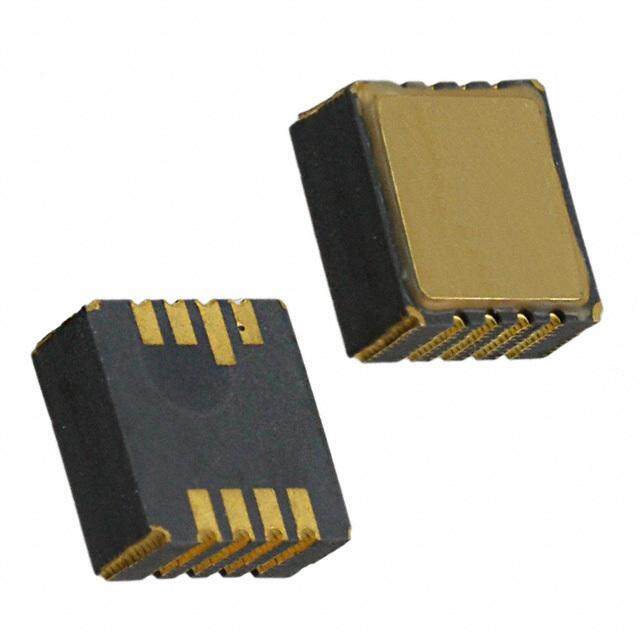
ICGOO在线商城 > 传感器,变送器 > 运动传感器 - 加速计 > ADIS16003CCCZ
- 型号: ADIS16003CCCZ
- 制造商: Analog
- 库位|库存: xxxx|xxxx
- 要求:
| 数量阶梯 | 香港交货 | 国内含税 |
| +xxxx | $xxxx | ¥xxxx |
查看当月历史价格
查看今年历史价格
ADIS16003CCCZ产品简介:
ICGOO电子元器件商城为您提供ADIS16003CCCZ由Analog设计生产,在icgoo商城现货销售,并且可以通过原厂、代理商等渠道进行代购。 ADIS16003CCCZ价格参考。AnalogADIS16003CCCZ封装/规格:运动传感器 - 加速计, Accelerometer X, Y Axis ±1.7g 1Hz ~ 2.25kHz 12-LGA (7.35x7.20)。您可以下载ADIS16003CCCZ参考资料、Datasheet数据手册功能说明书,资料中有ADIS16003CCCZ 详细功能的应用电路图电压和使用方法及教程。
| 参数 | 数值 |
| 产品目录 | |
| 描述 | IC ACCELEROMETER DUAL AXIS 12LGA加速计 Dual-Axis +/-1.7g w/ SPI IF |
| 产品分类 | 加速计运动与定位传感器 |
| 品牌 | Analog Devices Inc |
| 产品手册 | |
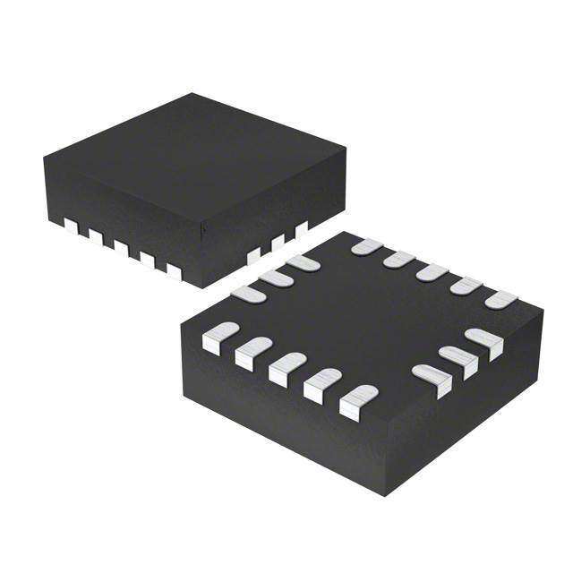
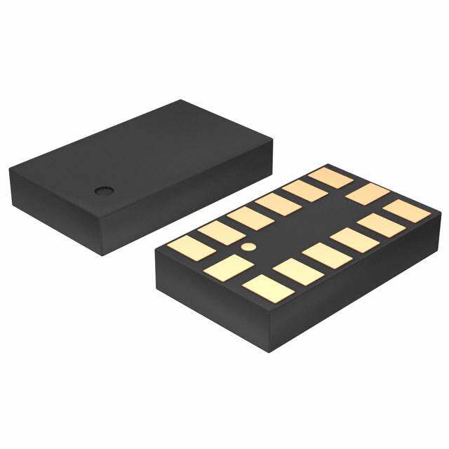
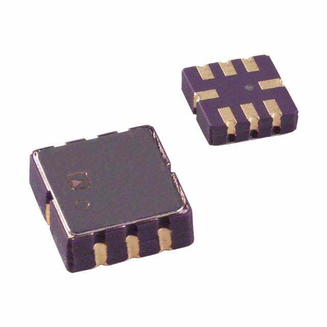
| 产品图片 |
|
| rohs | RoHS 合规性豁免不适用 / 符合限制有害物质指令(RoHS)规范要求 |
| 产品系列 | 加速计,Analog Devices ADIS16003CCCZ- |
| 数据手册 | |
| 产品型号 | ADIS16003CCCZ |
| 产品培训模块 | http://www.digikey.cn/PTM/IndividualPTM.page?site=cn&lang=zhs&ptm=38 |
| 产品目录页面 | |
| 产品种类 | 加速计 |
| 传感轴 | Dual |
| 供应商器件封装 | 12-LGA(7.35x7.20) |
| 分辨率 | 12 bit |
| 加速 | 1.7 g |
| 加速度范围 | ±1.7g |
| 商标 | Analog Devices |
| 安装类型 | 表面贴装 |
| 安装风格 | SMD/SMT |
| 封装 | Tray |
| 封装/外壳 | 12-BLGA |
| 封装/箱体 | LGA-12 |
| 工厂包装数量 | 260 |
| 带宽 | 1Hz ~ 2.25kHz 可选 |
| 接口 | SPI |
| 数字输出-位数 | 12 bit |
| 数字输出-总线接口 | SPI |
| 最大工作温度 | + 125 C |
| 最小工作温度 | - 40 C |
| 标准包装 | 1 |
| 灵敏度 | 820 LSB/g |
| 电压-电源 | 3 V ~ 5.25 V |
| 电源电压-最大 | 5.25 V |
| 电源电压-最小 | 3 V |
| 电源电流 | 1.5 uA |
| 系列 | ADIS16003 |
| 视频文件 | http://www.digikey.cn/classic/video.aspx?PlayerID=1364138032001&width=640&height=505&videoID=2245193160001http://www.digikey.cn/classic/video.aspx?PlayerID=1364138032001&width=640&height=505&videoID=2245193171001http://www.digikey.cn/classic/video.aspx?PlayerID=1364138032001&width=640&height=505&videoID=2245193161001http://www.digikey.cn/classic/video.aspx?PlayerID=1364138032001&width=640&height=505&videoID=2245193172001 |
| 轴 | X,Y |
| 输出类型 | SPI |
| 配用 | /product-detail/zh/ADIS16003%2FPCBZ/ADIS16003%2FPCBZ-ND/993137 |



- 商务部:美国ITC正式对集成电路等产品启动337调查
- 曝三星4nm工艺存在良率问题 高通将骁龙8 Gen1或转产台积电
- 太阳诱电将投资9.5亿元在常州建新厂生产MLCC 预计2023年完工
- 英特尔发布欧洲新工厂建设计划 深化IDM 2.0 战略
- 台积电先进制程称霸业界 有大客户加持明年业绩稳了
- 达到5530亿美元!SIA预计今年全球半导体销售额将创下新高
- 英特尔拟将自动驾驶子公司Mobileye上市 估值或超500亿美元
- 三星加码芯片和SET,合并消费电子和移动部门,撤换高东真等 CEO
- 三星电子宣布重大人事变动 还合并消费电子和移动部门
- 海关总署:前11个月进口集成电路产品价值2.52万亿元 增长14.8%



PDF Datasheet 数据手册内容提取
Dual-Axis ±1.7 g Accelerometer with SPI Interface Data Sheet ADIS16003 FEATURES GENERAL DESCRIPTION Dual-axis accelerometer The ADIS16003 is a low cost, low power, complete dual-axis SPI digital output interface accelerometer with an integrated serial peripheral interface Internal temperature sensor (SPI). An integrated temperature sensor is also available on the Highly integrated; minimal external components SPI interface. The ADIS16003 measures acceleration with a full- Bandwidth externally selectable scale range of ±1.7 g (minimum), and it can measure both dynamic 1 mg resolution at 60 Hz acceleration (vibration) and static acceleration (gravity). Externally controlled electrostatic self-test The typical noise floor is 110 μg/√Hz, allowing signals below 3.0 V to 5.25 V single-supply operation 1 mg (60 Hz bandwidth) to be resolved. Low power: <2 mA 3500 g shock survival The bandwidth of the accelerometer is set with optional capaci- 7.2 mm × 7.2 mm × 3.7 mm package tors CX and CY at the XFILT and YFILT pins. Selection of the two analog input channels is controlled via the serial interface. An externally driven self-test pin (ST) allows the user to verify APPLICATIONS the accelerometer functionality. Industrial vibration/motion sensing The ADIS16003 is available in a 7.2 mm × 7.2 mm × 3.7 mm, Platform stabilization 12-terminal LGA package. Dual-axis tilt sensing Tracking, recording, and analysis devices Alarms and security devices FUNCTIONAL BLOCK DIAGRAM VCC SCLK DUA±1L.-7AgXIS SERIAL DIN ACCELEROMETER INTERFACE DOUT CS CDC TCS TEMP SENSOR COM ST YFILT XFILT CY CX 056463-001 Figure 1. Rev. B Information furnished by Analog Devices is believed to be accurate and reliable. However, no responsibility is assumed by Analog Devices for its use, nor for any infringements of patents or other One Technology Way, P.O. Box 9106, Norwood, MA 02062-9106, U.S.A. rights of third parties that may result from its use. Specifications subject to change without notice. No license is granted by implication or otherwise under any patent or patent rights of Analog Devices. Tel: 781.329.4700 www.analog.com Trademarks and registered trademarks are the property of their respective owners. Fax: 781.461.3113 ©2005-2012 Analog Devices, Inc. All rights reserved.
ADIS16003 Data Sheet TABLE OF CONTENTS Features..............................................................................................1 Self-Test.......................................................................................11 Applications.......................................................................................1 Serial Interface............................................................................11 General Description.........................................................................1 Accelerometer Serial Interface..................................................11 Functional Block Diagram..............................................................1 Temperature Sensor Serial Interface........................................12 Revision History...............................................................................2 Power Supply Decoupling.........................................................12 Specifications.....................................................................................3 Setting the Bandwidth...............................................................13 Timing Specifications..................................................................4 Selecting Filter Characteristics: The Noise/Bandwidth Trade- Circuit and Timing Diagrams.....................................................5 Off.................................................................................................13 Absolute Maximum Ratings............................................................6 Applications Information..............................................................15 ESD Caution..................................................................................6 Dual-Axis Tilt Sensor................................................................15 Pin Configuration and Function Descriptions.............................7 Second Level Assembly.............................................................15 Typical Performance Characteristics.............................................8 Outline Dimensions.......................................................................16 Theory of Operation......................................................................11 Ordering Guide..........................................................................16 Accelerometer Data Format......................................................11 REVISION HISTORY 3/12—Rev. A to Rev. B Added Accelerometer Data Format Section and Table 6; Renumbered Sequentially..............................................................11 10/07—Rev. 0 to Rev. A Changes to Features and General Description.............................1 Added Note 6 to Table 2..................................................................4 Changes to Figure 5..........................................................................6 Changes to Serial Interface Section and Layout.........................11 Changes to Layout..........................................................................14 Deleted Figure 24 and Table 11.....................................................14 Changes to Converting Acceleration to Tilt Section and Second-Level Assembly Section...................................................15 Updated Outline Dimensions.......................................................16 Changes to Ordering Guide..........................................................16 10/05—Revision 0: Initial Version Rev. B | Page 2 of 16
Data Sheet ADIS16003 SPECIFICATIONS T = –40°C to +125°C, V = 5 V, C , C = 0 μF, acceleration = 0 g, unless otherwise noted. All minimum and maximum specifications are A CC X Y guaranteed. Typical specifications are not guaranteed. Table 1. Parameter Conditions Min Typ Max Unit ACCELEROMETER SENSOR INPUT Each axis Measurement Range1 ±1.7 g Nonlinearity % of full scale ±0.5 ±2.5 % Package Alignment Error ±1.5 Degrees Alignment Error X sensor to Y sensor ±0.1 Degrees Cross-Axis Sensitivity ±2 ±5 % ACCELEROMETER SENSITIVITY Each axis Sensitivity at XFILT, YFILT 769 820 885 LSB/g Sensitivity Change due to Temperature2 Delta from 25°C ±8 LSB ZERO g BIAS LEVEL Each axis 0 g Voltage at XFILT, YFILT 1905 2048 2190 LSB 0 g Offset vs. Temperature ±0.14 LSB/°C ACCELEROMETER NOISE PERFORMANCE Noise Density At 25°C 110 μg/√Hz rms ACCELEROMETER FREQUENCY RESPONSE3 C , C Range4 0 10 μF X Y R Tolerance 24 32 40 kΩ FILT Sensor Resonant Frequency 5.5 kHz ACCELEROMETER SELF-TEST Logic Input Low 0.2 × V V CC Logic Input High 0.8 × V V CC ST Input Resistance to COM 30 50 kΩ Output Change at X , Y 5 Self-Test 0 to Self-Test 1 323 614 904 LSB OUT OUT TEMPERATURE SENSOR Accuracy V = 3 V to 5.25 V ±2 °C CC Resolution 10 Bits Update Rate 400 μs Temperature Conversion Time 25 μs DIGITAL INPUT Input High Voltage (V ) V = 4.75 V to 5.25 V 2.4 V INH CC V = 3.0 V to 3.6 V 2.1 V CC Input Low Voltage (V ) V = 3.0 V to 5.25 V 0.8 V INL CC Input Current V = 0 V or V −10 +1 +10 μA IN CC Input Capacitance 10 pF DIGITAL OUTPUT Output High Voltage (V ) I = 200 μA, V = 3.0 V to 5.25 V V − 0.5 V OH SOURCE CC CC Output Low Voltage (V ) I = 200 μA 0.4 V OL SINK POWER SUPPLY Operating Voltage Range 3.0 5.25 V Quiescent Supply Current f = 50 kSPS 1.5 2.0 mA SCLK Power-Down Current 1.0 mA Turn-On Time6 C , C = 0.1 μF 20 ms X Y 1 Guaranteed by measurement of initial offset and sensitivity. 2 Defined as the output change from ambient-to-maximum temperature or ambient-to-minimum temperature. 3 Actual bandwidth response controlled by user-supplied external capacitor (CX, CY). 4 Bandwidth = 1/(2π × 32 kΩ × (2200 pF + C)). For CX, CY = 0 μF, bandwidth = 2260 Hz. For CX, CY = 10 μF, bandwidth = 0.5 Hz. Minimum/maximum values not tested. 5 Self-test response changes as the square of VCC. 6 Larger values of CX, CY increase turn-on time. Turn-on time is approximately 160 × (0.0022 μF + Cx + Cy) + 4 ms, where CX, CY are in μF. Rev. B | Page 3 of 16
ADIS16003 Data Sheet TIMING SPECIFICATIONS T = −40°C to +125°C, acceleration = 0 g, unless otherwise noted. A Table 2. Parameter1, 2 V = 3.3 V V = 5 V Unit Description CC CC f 3 10 10 kHz min SCLK 2 2 MHz max t 14.5 × t 14.5 × t CONVERT SCLK SCLK t 1.5 × t 1.5 × t Throughput time = t + t = 16 t ACQ SCLK SCLK CONVERT ACQ SCLK t 10 10 ns min TCS/CS to SCLK setup time 1 t 4 60 30 ns max Delay from TCS/CS until DOUT three-state disabled 2 t4 100 75 ns max Data access time after SCLK falling edge 3 t 20 20 ns min Data setup time prior to SCLK rising edge 4 t 20 20 ns min Data hold time after SCLK rising edge 5 t 0.4 × t 0.4 × t ns min SCLK high pulse width 6 SCLK SCLK t 0.4 × t 0.4 × t ns min SCLK low pulse width 7 SCLK SCLK t 5 80 80 ns max TCS/CS rising edge to DOUT high impedance 8 t 6 5 5 μs typ Power-up time from shutdown 9 1 Guaranteed by design. All input signals are specified with tr and tf = 5 ns (10% to 90% of VCC) and timed from a voltage level of 1.6 V. The 3.3 V operating range spans from 3.0 V to 3.6 V. The 5 V operating range spans from 4.75 V to 5.25 V. 2 See Figure 3 and Figure 4. 3 Mark/space ratio for the SCLK input is 40/60 to 60/40. 4 Measured with the load circuit in Figure 2 and defined as the time required for the output to cross 0.4 V or 2.0 V with VCC = 3.3 V and time for an output to cross 0.8 V or 2.4 V with VCC = 5.0 V. 5 t8 is derived from the measured time taken by the data outputs to change 0.5 V when loaded with the circuit in Figure 2. The measured number is then extrapolated back to remove the effects of charging or discharging the 50 pF capacitor. This means that the time, t8, quoted in the timing characteristics is the true bus relinquish time of the part and is independent of the bus loading. 6 Shut-down recovery time denotes the time it takes to start producing samples and does not account for the recovery time of the sensor, which is dependent on the overall bandwidth. Rev. B | Page 4 of 16
Data Sheet ADIS16003 CIRCUIT AND TIMING DIAGRAMS 200µA IOL TO OUTPUT 1.6V PIN CL 50pF 200µA IOH 05463-002 Figure 2. Load Circuit for Digital Output Timing Specifications tACQ tCONVERT CS t1 t6 SCLK 1 2 3 4 5 6 15 16 t2 t7 t3 t8 DOUTTHREE-STATE 4 LEADING ZEROS DB11 DB10 DB9 DB0 THREE-STATE t 4 t DIN DONTC5 ZERO ZERO ZERO ADD0 ONE ZERO PM0 05463-003 Figure 3. Accelerometer Serial Interface Timing Diagram TCS t1 t6 SCLK 1 2 3 4 11 15 16 THREE- t3 t7 t8 STATE THREE-STATE DOUT LEZAEDRIONG DB9 DB8 DB0 DIN 05463-004 Figure 4. Temperature Serial Interface Timing Diagram Rev. B | Page 5 of 16
ADIS16003 Data Sheet ABSOLUTE MAXIMUM RATINGS Table 4. Package Characteristics Table 3. Package Type θ θ Device Weight Parameter Rating JA JC 12-Terminal LGA 200°C/W 25°C/W 0.3 grams Acceleration (Any Axis, Unpowered) 3500 g Acceleration (Any Axis, Powered) 3500 g V −0.3 V to +7.0 V 3.1865 CC 8× All Other Pins (COM − 0.3 V) to (V + 0.3 V) 1.797 CC 8× Output Short-Circuit Duration 0.670 (Any Pin to Common) Indefinite 8× Operating Temperature Range −40°C to +125°C Storage Temperature Range −65°C to +150°C 6.373 3.594 2× 4× Stresses above those listed under Absolute Maximum Ratings may cause permanent damage to the device. This is a stress rating only; functional operation of the device at these or any other conditions above those indicated in the operational 0.500 1.127 12× section of this specification is not implied. Exposure to absolute 12× mdeavxicime ruemlia rbaitliintyg. conditions for extended periods may affect 7.2mm × 7.2mm STACKED LGA.ALL DIMENSIONS IN mm. 05463-023 Figure 5. Second-Level Assembly Pad Layout ESD CAUTION Rev. B | Page 6 of 16
Data Sheet ADIS16003 PIN CONFIGURATION AND FUNCTION DESCRIPTIONS K LC CC S S V C 12 11 10 TCS 1 9 XFILT ADIS16003 TOP VIEW DOUT 2 (Not to Scale) 8 YFILT DIN 3 7 NC 4 5 6 NC = NO MOCCONNECTCN TS 05463-005 Figure 6. Pin Configuration Table 5. Pin Function Descriptions Pin No. Mnemonic Description 1 TCS Temperature Chip Select. Active low logic input. This input frames the serial data transfer for the temperature sensor output. 2 DOUT Data Out, Logic Output. The conversion of the ADIS16003 is provided on this output as a serial data stream. The bits are clocked out on the falling edge of the SCLK input. 3 DIN Data In, Logic Input. Data to be written into the control register of the ADIS16003 is provided on this input and is clocked into the register on the rising edge of SCLK. 4 COM Common. Reference point for all circuitry on the ADIS16003. 5, 7 NC No Connect. 6 ST Self-Test Input. Active high logic input. Simulates a nominal 0.75 g test input for diagnostic purposes. 8 YFILT Y-Channel Filter Node. Used in conjunction with an optional external capacitor to band limit the ac signal from the accelerometer. 9 XFILT X-Channel Filter Node. Used in conjunction with an optional external capacitor to band limit the ac signal from the accelerometer. 10 CS Chip Select. Active low logic input. This input provides the dual function of initiating the accelerometer conversions on the ADIS16003 and frames the serial data transfer for the accelerometer output. 11 V Power Supply Input. The V range for the ADIS16003 is from 3.0 V to 5.25 V. CC CC 12 SCLK Serial Clock, Logic Input. SCLK provides the serial clock for accessing data from the part and writing serial data to the control register. This clock input is also used as the clock source for the conversion process of the ADIS16003. Rev. B | Page 7 of 16
ADIS16003 Data Sheet TYPICAL PERFORMANCE CHARACTERISTICS 890 40 35 870 N O TI 30 TIVITY (LSB/g)885300 GE OF POPULA 2250 NSI TA 15 E810 N S E C R 10 E P 790 770 05463-006 05 05463-009 –40 –20 0 20 40 60 80 100 125 1900 1929 1958 1987 2016 2045 2074 2103 2132 2161 2190 TEMPERATURE (°C) OUTPUT (LSB) Figure 7. Sensitivity vs. Temperature (ADIS16003 Soldered to PCB) Figure 10. X-Axis Zero g Bias at 25°C 2200 40 35 2150 N O TI 30 A B)2100 UL S P 25 L O VEL (2050 OF P 20 AS LE TAGE 15 BI2000 N E C R 10 E P 1950 1900 05463-007 05 05463-010 –40 –20 0 20 40 60 80 100 125 1990 1929 1958 1987 2016 2045 2074 2103 2132 2161 2190 TEMPERATURE (°C) OUTPUT (LSB) Figure 8. Zero g Bias vs. Temperature Figure 11. Y-Axis Zero g Bias at 25°C 2200 45 40 2150 N O 35 TI A B)2100 UL 30 S P L O VEL (2050 OF P 25 AS LE TAGE 20 BI2000 N 15 E C R E 10 P 1950 1900 05463-008 05 05463-011 2.8 3.0 3.2 3.4 3.6 3.8 4.0 4.2 4.4 4.6 4.8 5.0 5.2 5.4 60 70 80 90 100 110 120 130 140 150 VCC (V) X-AXIS NOISE DENSITY (µg/ Hz) Figure 9. Zero g Bias vs. Supply Figure 12. X-Axis Noise Density at 25°C Rev. B | Page 8 of 16
Data Sheet ADIS16003 50 60 50 N 40 N O O TI TI A A UL UL 40 P P O 30 O P P OF OF 30 E E G G A 20 A T T N N 20 E E C C R R PE 10 PE 10 0 05463-012 0 05463-015 60 70 80 90 100 110 120 130 140 150 350 400 450 500 550 600 650 700 750 800 850 Y-AXIS NOISE DENSITY (mg/ Hz) OUTPUT (LSB) Figure 13. Y-Axis Noise Density at 25°C Figure 16. Self-Test at 25°C, VCC at 5.0 V 35 45 40 30 N N O O 35 ATI 25 ATI UL UL 30 P P O O P 20 P 25 F F O O GE 15 GE 20 A A T T N N 15 CE 10 CE R R E E 10 P P 5 0 05463-013 05 05463-016 –4.5 –3.5 –2.5 –1.5 –0.5 0.5 1.5 2.5 3.5 4.5 5.5 180 195 210 225 240 255 270 285 300 315 PERCENT SENSITIVITY (%) OUTPUT (LSB) Figure 14. Z vs. X Cross-Axis Sensitivity Figure 17. Self-Test at 25°C, VCC at 3.3 V 40 750 35 700 N O ATI 30 B/g) OPUL 25 L (LS 650 P E OF 20 LEV 600 E T G S TA 15 TE CEN ELF- 550 R 10 S E P 500 05 05463-014 450 05463-017 –4.5 –3.5 –2.5 –1.5 –0.5 0.5 1.5 2.5 3.5 4.5 5.5 –40 –20 0 20 40 60 80 100 125 PERCENT SENSITIVITY (%) TEMPERATURE(°C) Figure 15. Z vs. Y Cross-Axis Sensitivity Figure 18. Self-Test vs. Temperature, VCC at 5.0 V Rev. B | Page 9 of 16
ADIS16003 Data Sheet 800 90 3.3V 80 700 N O 70 VEL (LSB) 650000 POPULATI 5600 5V SELF-TEST LE 430000 RCENTAGE OF 4300 E 20 P 200 100 05463-018 100 05463-020 2.8 3.0 3.2 3.4 3.6 3.8 4.0 4.2 4.4 4.6 4.8 5.0 5.2 5.4 1.151.201.251.301.351.401.451.501.551.601.651.701.75 VCC (V) CURRENT (µA) Figure 19. Self-Test vs. Supply Voltage Figure 21. Supply Current at 25°C 1.8 1.0 1.7 0.8 0.6 1.6 CURRENT (mA) 11..54 TA = +125°C TA = +25°C G ERROR (dB) 00..042 LY 1.3 LIN –0.2 P P P M SU 1.2 TA = –40°C SA –0.4 –0.6 11..01 05463-019 ––01..80 05463-021 2.8 3.0 3.2 3.4 3.6 3.8 4.0 4.2 4.4 4.6 4.8 5.0 5.2 5.4 1 10 100 VCC (V) SAMPLE RATE (kSPS) Figure 20. Supply Current vs. Supply Voltage Figure 22. Sampling Error vs. Sample Rate Rev. B | Page 10 of 16
Data Sheet ADIS16003 THEORY OF OPERATION The ADIS16003 is a low cost, low power, complete dual-axis the next digital conversion is initiated. The details for the control accelerometer with an integrated serial peripheral interface register bit functions are shown in Table 7. (SPI) and an integrated temperature sensor whose output is Accelerometer Control Register also available on the SPI interface. The ADIS16003 is capable MSB LSB of measuring acceleration with a full-scale range of ±1.7 g DONTC ZERO ZERO ZERO ADD0 ONE ZERO PM0 (minimum). It can also measure both dynamic acceleration (vibration) and static acceleration (gravity). Table 7. Accelerometer Control Register Bit Functions ACCELEROMETER DATA FORMAT Bit Mnemonic Comments 7 DONTC Don’t care. Can be 1 or 0. The accelerometer data comes out in a 12-bit, offset-binary format. 6 to 4 ZERO These bits should be held low. See Table 6 for examples of this data format. 3 ADD0 This address bit selects the x-axis or y-axis outputs. A 0 selects the x-axis; Table 6. Acceleration Data Format Examples a 1 selects the y-axis. Acceleration (g) Decimal Hex Binary 2 ONE This bit should be held high. +1.7 3442 0xD72 1101 0111 0010 1 ZERO This bit should be held low. +2/+820 2050 0x802 1000 0000 0010 0 PM0 This bit selects the operation mode for +1/+820 2049 0x801 1000 0000 0001 the accelerometer; set to 0 for normal 0 2048 0x800 1000 0000 0000 operation and 1 for power-down mode. −1/+820 2047 0x7FF 0111 1111 1111 −2/+820 2046 0x7FE 0111 1111 1110 Power Down −1.7 654 0x28E 0010 1000 1110 By setting PM0 to 1 when updating the accelerometer SELF-TEST control register, the ADIS16003 goes into a shutdown mode. The information stored in the control register is maintained The ST pin controls the self-test feature. When this pin is set to V , CC during shutdown. The ADIS16003 changes modes as soon as an electrostatic force is exerted on the beam of the accelerometer. the control register is updated. If the part is in shutdown mode The resulting movement of the beam allows the user to test if and PM0 is changed to 0, the part powers up on the 16th SCLK the accelerometer is functional. The typical change in output is rising edge. 750 mg (corresponding to 614 LSB) for V = 5.0 V. This pin can be CC left open-circuit or connected to common in normal use. The ST ADD0 pin should never be exposed to a voltage greater than V + 0.3 V. CC By setting ADD0 to 0 when updating the accelerometer control If the system design is such that this condition cannot be register, the x-axis output is selected. By setting ADD0 to 1, guaranteed (for example, multiple supply voltages are present), the y-axis output is selected. a low V clamping diode between ST and V is recommended. F CC ZERO SERIAL INTERFACE ZERO is defined as the Logic low level. The serial interface on the ADIS16003 consists of five wire: CS, ONE TCS, SCLK, DIN, and DOUT. Both accelerometer axes and the ONE is defined as the Logic high level. temperature sensor data are available on the serial interface. The CS and TCS are used to select the accelerometer or temperature DONTC sensor outputs, respectively. CS and TCS cannot be active at the DONTC is defined as don’t care and can be a low or high same time. logic level. The SCLK input accesses data from the internal data registers. Accelerometer Conversion Details ACCELEROMETER SERIAL INTERFACE Every time the accelerometer is sampled, the sampling function discharges the internal C or C filtering capacitors by up to 2% Figure 3 shows the detailed timing diagram for serial interfacing to X Y of their initial values (assuming no additional external filtering the accelerometer in the ADIS16003. The serial clock provides the capacitors are added). The recovery time for the filter capacitor conversion clock. CS initiates the data transfer and conversion to recharge is approximately 10 μs. Therefore, sampling the process and also frames the serial data transfer for the accelerometer at a rate of 10 kSPS or less does not induce a accelerometer output. The accelerometer output is sampled on the sampling error. However, as sampling frequencies increase second rising edge of the SCLK input after the falling edge of CS. above 10 kSPS, one can expect sampling errors to attenuate The conversion requires 16 SCLK cycles to complete. The rising the actual acceleration levels. edge of CS puts the bus back into three-state. If CS remains low, Rev. B | Page 11 of 16
ADIS16003 Data Sheet TEMPERATURE SENSOR SERIAL INTERFACE Temperature Sensor Conversion Details Read Operation The ADIS16003 features a 10-bit digital temperature sensor that allows an accurate measurement of the ambient device Figure 4 shows the timing diagram for a serial read from the temperature to be made. temperature sensor. The TCS line enables the SCLK input. Ten bits of data and a leading zero are transferred during a read The conversion clock for the temperature sensor is internally operation. Read operations occur during streams of 16 clock generated so no external clock is required except when reading pulses. The serial data is accessed in a number of bytes if 10 bits from and writing to the serial port. In normal mode, an internal of data are being read. At the end of the read operation, the clock oscillator runs the automatic conversion sequence. A DOUT line remains in the state of the last bit of data clocked conversion is initiated approximately every 350 μs. At this time, out until TCS goes high, at which time the DOUT line from the temperature sensor wakes up and performs a temperature the temperature sensor goes three-state. conversion. This temperature conversion typically takes 25 μs, at which time the temperature sensor automatically shuts down. Write Operation The result of the most recent temperature conversion is available Figure 4 also shows the timing diagram for the serial write in the serial output register at any time. Once the conversion is to the temperature sensor. The write operation takes place at finished, an internal oscillator starts counting and is designed to the same time as the read operation. Data is clocked into the time out every 350 μs. The temperature sensor then powers up control register on the rising edge of SCLK. DIN should remain and does a conversion. If the TCS is brought low every 350 μs low for the entire cycle. (±30%) or less, the same temperature value is output onto the Temperature Sensor Control Register DOUT line every time without changing. MSB LSB It is recommended that the TCS line not be brought low every ZERO ZERO ZERO ZERO ZERO ZERO ZERO ZERO 350 μs (±30%) or less. The ±30% covers process variation. The TCS should become active (high to low) outside this range. Table 8. Temperature Sensor Control Register Bit Functions The device is designed to autoconvert every 350 μs. If the Bit Mnemonic Comments temperature sensor is accessed during the conversion process, 7 to 0 ZERO All bits should be held low. an internal signal is generated to prevent any update of the temperature value register during the conversion. This prevents ZERO the user from reading back spurious data. The design of this ZERO is defined as the Logic low level. feature results in this internal lockout signal being reset only at Output Data Format the start of the next autoconversion. Therefore, if the TCS line goes active before the internal lockout signal is reset to its inactive The output data format for the temperature sensor is twos mode, the internal lockout signal is not reset. To ensure that no complement. Table 9 shows the relationship between the lockout signal is set, bring TCS low at a greater time than 350 μs temperature and the digital output. (±30%). As a result, the temperature sensor is not interrupted Table 9. Temperature Sensor Data Format during a conversion process. Temperature Digital Output (DB9 … DB0) In the automatic conversion mode, every time a read or write −40°C 11 0110 0000 operation takes place, the internal clock oscillator is restarted at −25°C 11 1001 1100 the end of the read or write operation. The result of the conver- −0.25°C 11 1111 1111 sion is typically available 25 μs later. Reading from the device 0°C 00 0000 0000 before conversion is complete provides the same set of data. +0.25°C 00 0000 0001 POWER SUPPLY DECOUPLING +10°C 00 0010 1000 +25°C 00 0110 0100 For most applications, a single 0.1 μF capacitor (CDC) adequately +50°C 00 1100 1000 decouples the accelerometer from noise on the power supply. +75°C 01 0010 1100 However, in some cases, particularly where noise is present at +100°C 01 1001 0000 the 140 kHz internal clock frequency (or any harmonic thereof), +125°C 01 1111 0100 noise on the supply can cause interference on the ADIS16003 output. If additional decoupling is needed, ferrite beads can be inserted in the supply line of the ADIS16003. Additionally, a larger bulk bypass capacitor (in the 1 μF to 22 μF range) can be added in parallel to CDC. Rev. B | Page 12 of 16
Data Sheet ADIS16003 SETTING THE BANDWIDTH SELECTING FILTER CHARACTERISTICS: THE NOISE/BANDWIDTH TRADE-OFF The ADIS16003 has provisions for band limiting the accelerometer. Capacitors can be added at the XFILT pin The accelerometer bandwidth selected ultimately determines and the YFILT pin to implement further low-pass filtering for the measurement resolution (smallest detectable acceleration). antialiasing and noise reduction. The equation for the 3 dB Filtering can be used to lower the noise floor, which improves bandwidth is the resolution of the accelerometer. Resolution is dependent on the analog filter bandwidth at XFILT and YFILT. f = 1/(2π(32 kΩ) × (C + 2200 pF)) −3dB (XFILT, YFILT) The ADIS16003 has a typical bandwidth of 2.25 kHz with no or more simply, external filtering. The analog bandwidth can be further f = 5 μF/(C + 2200 pF) −3dB (XFILT, YFILT) decreased to reduce noise and improve resolution. The tolerance of the internal resistor (R ) can vary typically FILT The ADIS16003 noise has the characteristics of white Gaussian as much as ±25% of its nominal value (32 kΩ); thus, the noise, which contributes equally at all frequencies and is described bandwidth varies accordingly. in terms of μg/√Hz (that is, the noise is proportional to the A minimum capacitance of 0 pF for CXFILT and CYFILT is allowable. square root of the bandwidth of the accelerometer). The user should limit bandwidth to the lowest frequency needed by the Table 10. Filter Capacitor Selection, CXFILT and CYFILT application to maximize the resolution and dynamic range of Bandwidth (Hz) Capacitor (μF) the accelerometer. 1 4.7 With the single-pole, roll-off characteristic, the typical noise of 10 0.47 the ADIS16003 is determined by 50 0.10 100 0.047 rmsNoise = (110 μg/√Hz) × (√(BW × 1.6)) 200 0.022 At 100 Hz, the noise is 400 0.01 rmsNoise = (110 μg/√Hz) × (√(100 × 1.6)) =1.4 mg 2250 0 Often, the peak value of the noise is desired. Peak-to-peak noise can only be estimated by statistical methods. Table 11 is useful for estimating the probabilities of exceeding various peak values, given the rms value. Table 11. Estimation of Peak-to-Peak Noise Percentage of Time Noise Exceeds Peak-to-Peak Value Nominal Peak-to-Peak Value (%) 2 × rms 32 4 × rms 4.6 6 × rms 0.27 8 × rms 0.006 Rev. B | Page 13 of 16
ADIS16003 Data Sheet 12 11 10 1 9 DIGITAL OUTPUT (IN LSBs) 2 X-AXIS: 1229 8 Y-AXIS: 2048 3 7 4 5 6 9 8 7 3 2 1 10 6 4 12 DIGITAL OUTPUT (IN LSBs) DIGITAL OUTPUT (IN LSBs) 11 XY--AAXXIISS:: 22806478 5 NoTot ptoV Siecwale 5 XY--AAXXIISS:: 12202498 11 12 4 6 10 1 2 3 7 8 9 6 5 4 7 3 DIGITAL OUTPUT (IN LSBs) DIGITAL OUTPUT (IN LSBs) 8 X-AXIS: 2867 2 X-AXIS: 2048 Y-AXIS: 2048 Y-AXIS: 2048 9 1 10 11 12 05463-024 Figure 23. Output Response vs. Orientation Rev. B | Page 14 of 16
Data Sheet ADIS16003 APPLICATIONS INFORMATION DUAL-AXIS TILT SENSOR Converting Acceleration to Tilt One of the most popular applications of the ADIS16003 is tilt When the accelerometer is oriented, so both its x-axis and measurement. An accelerometer uses the force of gravity as an y-axis are parallel to the earth’s surface, it can be used as a input vector to determine the orientation of an object in space. 2-axis tilt sensor with a roll axis and a pitch axis. Once the An accelerometer is most sensitive to tilt when its sensitive axis output signal from the accelerometer is converted to an is perpendicular to the force of gravity, that is, parallel to the acceleration that varies between –1 g and +1 g, the output earth’s surface. At this orientation, its sensitivity to changes in tilt is tilt in degrees is calculated as follows: highest. When the accelerometer is oriented on axis to gravity, PITCH = Asin(A /1 g) X near its +1 g or –1 g reading, the change in output acceleration per ROLL = Asin(A /1 g) degree of tilt is negligible. When the accelerometer is perpendicular Y to gravity, its output changes nearly 17.5 mg per degree of tilt. where: At 45°, its output changes at only 12.2 mg per degree and its AX is the acceleration along the x-axis. resolution declines. AY is the acceleration along the y-axis. Be sure to account for overranges. It is possible for the accelerometers to output a signal greater than ±1 g due to vibration, shock, or other accelerations. SECOND LEVEL ASSEMBLY The ADIS16003 can be attached to the second level assembly board using SN63 (or equivalent) or lead-free solder. IPC/ JEDEC J-STD-020 and J-STD-033 provide standard handling procedures for these types of packages. Rev. B | Page 15 of 16
ADIS16003 Data Sheet OUTLINE DIMENSIONS 3.594 BSC 1.797 (4×) PIN 1 7.35 BSC INDICATOR MAX (8×) 1.00 BSC 10 12 (12×) 9 1 6 .373 7.20 BSC TYP (2×) 7 3 0.797 BSC 6 4 (8×) TOP VIEW 0.200 BOTTOM VIEW 0.373 BSC MIN (12×) (ALL SIDES) 5.00 TYP 3.70 MAX SIDE VIEW 092407-C Figure 24. 12-Terminal Land Grid Array [LGA] (CC-12-1) Dimensions shown in millimeters ORDERING GUIDE Model1 Temperature Range Package Description Package Option ADIS16003CCCZ −40°C to +125°C 12-Terminal Land Grid Array (LGA) CC-12-1 ADIS16003/PCBZ Evaluation Board 1 Z = RoHS Compliant Part. ©2005-2012 Analog Devices, Inc. All rights reserved. Trademarks and registered trademarks are the property of their respective owners. D05463-0-3/12(B) Rev. B | Page 16 of 16

 Datasheet下载

