ICGOO在线商城 > 射频/IF 和 RFID > RF 开关 > ADG902BRMZ

 Datasheet下载
- 型号: ADG902BRMZ
- 制造商: Analog
- 库位|库存: xxxx|xxxx
- 要求:
| 数量阶梯 | 香港交货 | 国内含税 |
| +xxxx | $xxxx | ¥xxxx |
查看当月历史价格
查看今年历史价格
ADG902BRMZ产品简介:
ICGOO电子元器件商城为您提供ADG902BRMZ由Analog设计生产,在icgoo商城现货销售,并且可以通过原厂、代理商等渠道进行代购。 ADG902BRMZ价格参考¥10.21-¥10.59。AnalogADG902BRMZ封装/规格:RF 开关, 射频开关 IC 通用 SPST 2.5GHz 50 欧姆 8-MSOP。您可以下载ADG902BRMZ参考资料、Datasheet数据手册功能说明书,资料中有ADG902BRMZ 详细功能的应用电路图电压和使用方法及教程。
| 参数 | 数值 |
| 产品目录 | |
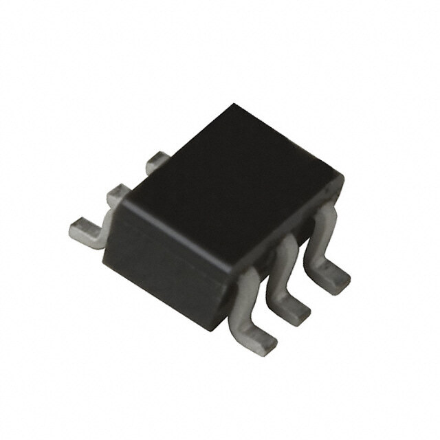
| 描述 | IC SWITCH SPST 1.65-2.75V 8-MSOPRF 开关 IC SGL WB 43dB Iso 1GHz CMOS 1.65-2.75V |
| 产品分类 | |
| IIP3 | 36dBm (标准) |
| 品牌 | Analog Devices Inc |
| 产品手册 | |
| 产品图片 |
|
| rohs | 符合RoHS无铅 / 符合限制有害物质指令(RoHS)规范要求 |
| 产品系列 | RF集成电路,RF 开关 IC,Analog Devices ADG902BRMZ- |
| 数据手册 | |
| P1dB | 17dBm (标准) P1dB |
| 产品型号 | ADG902BRMZ |
| RF类型 | 通用 |
| 产品培训模块 | http://www.digikey.cn/PTM/IndividualPTM.page?site=cn&lang=zhs&ptm=15131 |
| 产品目录页面 | |
| 产品种类 | RF 开关 IC |
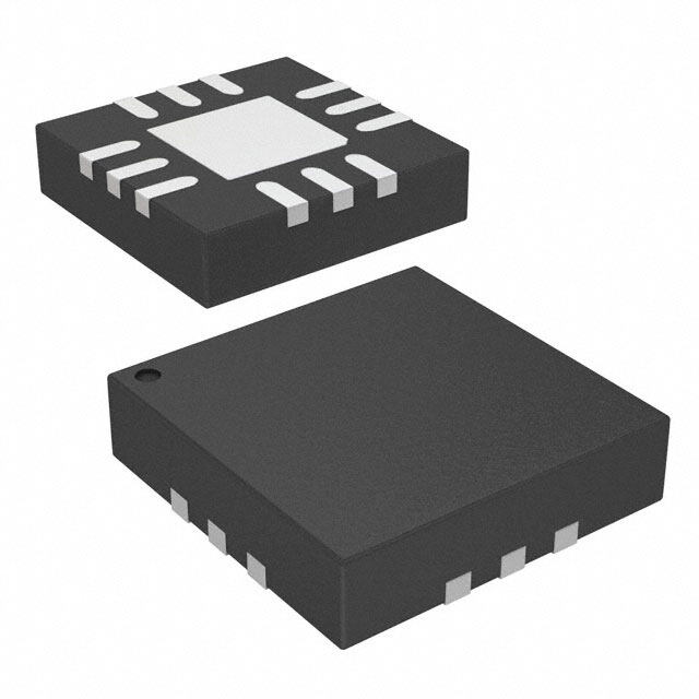
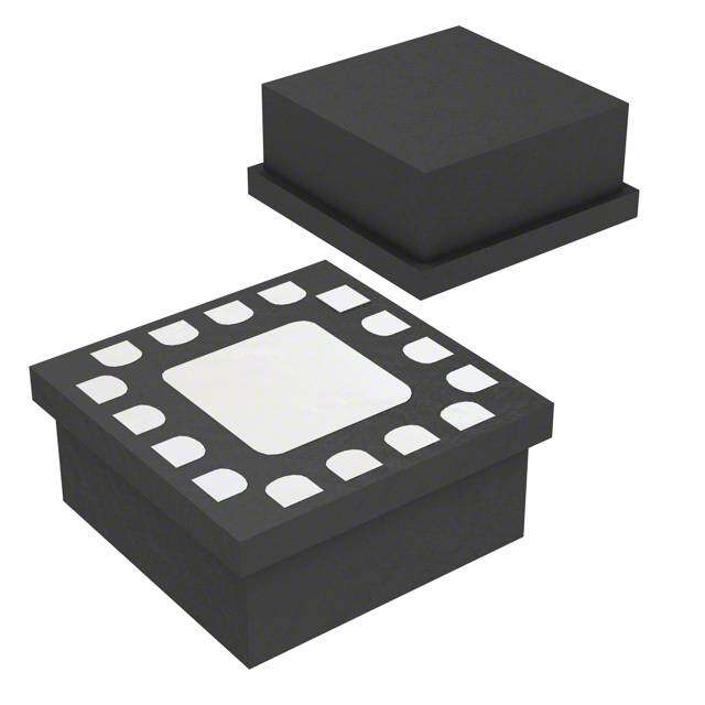
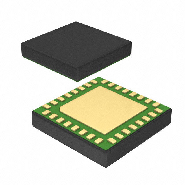
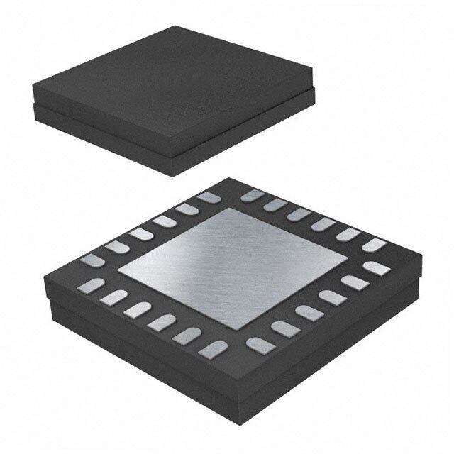
| 供应商器件封装 | 8-MSOP |
| 包装 | 管件 |
| 商标 | Analog Devices |
| 安装风格 | SMD/SMT |
| 封装 | Tube |
| 封装/外壳 | 8-TSSOP,8-MSOP(0.118",3.00mm 宽) |
| 封装/箱体 | MSOP-8 |
| 工作温度 | -40°C ~ 85°C |
| 工厂包装数量 | 50 |
| 开关数量 | Single |
| 开关配置 | SPST |
| 拓扑 | 反射 |
| 插损@频率 | 0.8dB @ 1GHz |
| 最大功率耗散 | 2.5 uW |
| 最大工作温度 | + 85 C |
| 最小工作温度 | - 40 C |
| 标准包装 | 50 |
| 特性 | - |
| 电压-电源 | 1.65 V ~ 2.75 V |
| 电源电压-最大 | 2.75 V |
| 电源电压-最小 | V |
| 电路 | SPST |
| 空闲时间—最大值 | 5.8 ns |
| 系列 | ADG902 |
| 视频文件 | http://www.digikey.cn/classic/video.aspx?PlayerID=1364138032001&width=640&height=505&videoID=2245193150001 |
| 运行时间—最大值 | 3.6 ns |
| 阻抗 | 50 欧姆 |
| 隔离@频率 | 40dB @ 1GHz (标准) |
| 频率 -上 | 2.5GHz |
| 频率 -下 | DC |


- 商务部:美国ITC正式对集成电路等产品启动337调查
- 曝三星4nm工艺存在良率问题 高通将骁龙8 Gen1或转产台积电
- 太阳诱电将投资9.5亿元在常州建新厂生产MLCC 预计2023年完工
- 英特尔发布欧洲新工厂建设计划 深化IDM 2.0 战略
- 台积电先进制程称霸业界 有大客户加持明年业绩稳了
- 达到5530亿美元!SIA预计今年全球半导体销售额将创下新高
- 英特尔拟将自动驾驶子公司Mobileye上市 估值或超500亿美元
- 三星加码芯片和SET,合并消费电子和移动部门,撤换高东真等 CEO
- 三星电子宣布重大人事变动 还合并消费电子和移动部门
- 海关总署:前11个月进口集成电路产品价值2.52万亿元 增长14.8%


PDF Datasheet 数据手册内容提取
0 Hz to 4.5 GHz, 40 dB Off Isolation at 1 GHz, 17 dBm P1dB at 1 GHz SPST Switches Data Sheet ADG901/ADG902 FEATURES FUNCTIONAL BLOCK DIAGRAMS ADG901 absorptive switch ADG901 ADG902 reflective switch RF1 RF2 Enables user to pass dc signals up to 0.5 V without dc blocking capacitor Operational from 0 Hz up to 4.5 GHz at −3 dB frequency 40 dB off isolation at 1 GHz typical 50Ω 50Ω 0.8 dB insertion loss at 1 GHz typical 17 dBm P1dB at 1 GHz typical A<1va μiAla bploew ine r3 c monmsu ×m 3p mtimon, 8-lead MSOP and 8-lead LFCSP CTRL 03336-001 CMOS/LVTTL control logic Figure 1. ADG901 Specified at 1.65 V to 2.75 V ADG902 APPLICATIONS RF1 RF2 Wireless communications General purpose RF switching Dual-band applications High speed filter selection Digital transceiver front-end switch ITFu snwerit mchoindgu les CTRL 03336-102 Antenna diversity switching list Figure 2. ADG902 GENERAL DESCRIPTION PRODUCT HIGHLIGHTS The ADG901/ADG902 are wideband switches that use a comple- mentary metal-oxide semiconductor (CMOS) process to provide 1. 40 dB Off Isolation at 1 GHz high isolation and low insertion loss to 1 GHz. The ADG901 is an 2. 0.8 dB Insertion Loss at 1 GHz absorptive (matched) switch with 50 Ω terminated shunt legs, while 3. 17 dBm P1dB at 1 GHz the ADG902 is a reflective switch. These devices are designed 0 such that the isolation is high over the dc to 1 GHz frequency TA = 25C –10 range. These switches enable the user to pass dc signals up to 0.5 V –20 without the use of a dc blocking capacitor. They have on-board CMOS control logic, thus eliminating the need for external –30 B) controlling circuitry. The control inputs are both CMOS and d –40 N ( LVTTL compatible. The low power consumption of these CMOS TIO –50 devices makes them ideally suited to wireless applications and OLA –60 VDD =2.5V general-purpose high frequency switching. IS –70 –80 –1–0900 VDD =1.8V 03336-002 10k 100k 1M 10M 100M 1G 10G FREQUENCY (Hz) Figure 3. Off Isolation vs. Frequency Rev. D Document Feedback Information furnished by Analog Devices is believed to be accurate and reliable. However, no responsibility is assumed by Analog Devices for its use, nor for any infringements of patents or other One Technology Way, P.O. Box 9106, Norwood, MA 02062-9106, U.S.A. rights of third parties that may result from its use. Specifications subject to change without notice. No license is granted by implication or otherwise under any patent or patent rights of Analog Devices. Tel: 781.329.4700 ©2003–2017 Analog Devices, Inc. All rights reserved. Trademarks and registered trademarks are the property of their respective owners. Technical Support www.analog.com
ADG901/ADG902 Data Sheet TABLE OF CONTENTS Features .............................................................................................. 1 ESD Caution...................................................................................5 Applications ....................................................................................... 1 Pin Configurations and Function Descriptions ............................6 Functional Block Diagrams ............................................................. 1 Typical Performance Characteristics ..............................................7 General Description ......................................................................... 1 Terminology .......................................................................................9 Product Highlights ........................................................................... 1 Test Circuits ..................................................................................... 10 Revision History ............................................................................... 2 Applications Information .............................................................. 11 Specifications ..................................................................................... 3 Absorptive vs. Reflective Switches ........................................... 11 Continous Current Per Channel ................................................ 4 ADG901/ADG902 Evaluation Board .......................................... 12 Absolute Maximum Ratings ............................................................ 5 Outline Dimensions ....................................................................... 13 Ordering Guide .......................................................................... 13 REVISION HISTORY 11/2017—Rev. C to Rev. D 10/2005—Rev. A to Rev. B Deleted Figure 3; Renumbered Sequentially ................................. 1 Changes to Figure 1 ........................................................................... 1 Added Figure 2; Renumbered Sequentially ................................. 1 Changes to Table 1 ............................................................................. 3 Changes to Features Section, Figure 1, General Description Changes to Ordering Guide .......................................................... 12 Section, and Product Highlights Section ...................................... 1 Deleted Endnote 4, Table 1; Renumbered Sequentially .............. 3 10/2004—Rev. 0 to Rev. A Change to −3 dB Frequency Parameter, Table 1 ........................... 3 Changes to Features ......................................................................... 1 Added Table 2; Renumbered Sequentially .................................... 4 Changes to Product Highlights ...................................................... 1 Changes to Table 3 ............................................................................ 5 Changes to Specifications ................................................................. 2 Change to Figure 4 ........................................................................... 6 Changes to Ordering Guide ............................................................. 3 Changes to Ordering Guide .......................................................... 12 Change to ADG9xx Evaluation Board Section ............................. 9 Changes to Ordering Guide .......................................................... 10 5/2016—Rev. B to Rev. C Changes to Figure 4 and Table 3 ..................................................... 5 8/2003—Revision 0: Initial Version Added Figure 5; Renumbered Sequentially .................................. 5 Updated Outline Dimensions ....................................................... 12 Changes to Ordering Guide .......................................................... 13 Rev. D | Page 2 of 13
Data Sheet ADG901/ADG902 SPECIFICATIONS V = 1.65 V to 2.75 V, GND = 0 V, input power = 0 dBm, all specifications T to T , unless otherwise specified.1 DD MIN MAX Table 1. B Version Parameter Symbol Test Conditions/Comments Min Typ2 Max Unit AC ELECTRICAL CHARACTERISTICS Operating Frequency3 DC 2.5 GHz −3 dB Frequency 4.5 GHz Input Power 0 V dc bias 7 dBm 0.5 V dc bias 16 dBm Insertion Loss S , S DC to 100 MHz; V = 2.5 V ± 10% 0.4 0.7 dB 21 12 DD 500 MHz; V = 2.5 V ± 10% 0.5 0.8 dB DD 1000 MHz; V = 2.5 V ± 10% 0.8 1.25 dB DD Isolation—RF1 to RF2 S , S 100 MHz 60 61 dB 21 12 CP Package 500 MHz 43 45 dB 1000 MHz 34 40 dB Isolation—RF1 to RF2 S , S 100 MHz 51 60 dB 21 12 RM Package 500 MHz 37.5 47 dB 1000 MHz 31 37 dB Return Loss (On Channel) S , S DC to 100 MHz 20 28 dB 11 22 500 MHz 23 29 dB 1000 MHz 25 28 dB Return Loss (Off Channel) S , S DC to 100 MHz 18 23 dB 11 22 500 MHz 17 21 dB 1000 MHz 15 19 dB On Switching Time t 50% CTRL to 90% RF 3.6 6 ns ON Off Switching Time t 50% CTRL to 10% RF 5.8 9.5 ns OFF Rise Time t 10% to 90% RF 3.1 5.5 ns RISE Fall Time t 90% to 10% RF 6.0 8.5 ns FALL 1 dB Compression P1dB 1000 MHz 17 dBm Third-Order Intermodulation Intercept IP3 900 MHz/901 MHz, 4 dBm 28.5 36 dBm Video Feedthrough4 2.5 mV p-p DC ELECTRICAL CHARACTERISTICS Input High Voltage V V = 2.25 V to 2.75 V 1.7 V INH DD V V = 1.65 V to 1.95 V 0.65 V V INH DD DD Input Low Voltage V V = 2.25 V to 2.75 V 0.7 V INL DD V V = 1.65 V to 1.95 V 0.35 V INL DD V DD Input Leakage Current I 0 ≤ V ≤ 2.75 V ±0.1 ±1 µA I IN CAPACITANCE RF1/RF2, RF Port On Capacitance C on f = 1 MHz 1.2 pF RF CTRL Input Capacitance C f = 1 MHz 2.1 pF CTRL POWER REQUIREMENTS V 1.65 2.75 V DD Quiescent Power Supply Current I Digital inputs = 0 V or V 0.1 1 µA DD DD 1 Temperature range for B version: −40°C to +85°C. 2 Typical values are at VDD = 2.5 V and 25°C, unless otherwise specified. 3 Point at which insertion loss degrades by 1 dB. 4 The dc transience at the output of any port of the switch when the control voltage is switched from high to low or low to high in a 50 Ω test setup, measured with 1 ns rise time pulses and 500 MHz bandwidth. Rev. D | Page 3 of 13
ADG901/ADG902 Data Sheet CONTINOUS CURRENT PER CHANNEL Table 2. Parameter 25°C 85°C 105°C 125°C Unit Test Conditions/Comments CONTINUOUS CURRENT PER CHANNEL 8-Lead LFCSP θ = 48°C/W, dc bias = 0.5 V JA V = 2.75 V, V = 0 V 70 7 3.85 2.8 mA maximum DD SS V = 1.65 V, V = 0 V 56 7 3.85 2.1 mA maximum DD SS 8-lead MSOP θ = 206°C/W, dc bias = 0.5 V JA V = 2.75 V, V = 0 V 51.1 7 3.85 2.8 mA maximum DD SS V = 1.65 V, V = 0 V 39.9 7 3.85 2.1 mA maximum DD SS Rev. D | Page 4 of 13
Data Sheet ADG901/ADG902 ABSOLUTE MAXIMUM RATINGS T = 25°C, unless otherwise specified. A Stresses at or above those listed under Absolute Maximum Ratings may cause permanent damage to the product. This is a Table 3. stress rating only; functional operation of the product at these Parameter Rating or any other conditions above those indicated in the operational VDD to GND −0.5 V to +4 V section of this specification is not implied. Operation beyond Inputs to GND −0.5 V to VDD + 0.3 V1 the maximum operating conditions for extended periods may Continuous Current Data2 + 15% affect product reliability. Input Power3 18 dBm Operating Temperature Range ESD CAUTION Industrial (B Version) −40°C to +85°C Storage Temperature Range −65°C to +150°C Junction Temperature 150°C θ Thermal Impedance JA MSOP Package 206°C/W LFCSP Package 2-Layer Board 84°C/W 4-Layer Board 48°C/W Lead Temperature, Soldering (10 sec) 300°C IR Reflow, Peak Temperature (<20 sec) 235°C ESD 1 kV 1 RF1/RF2 off port inputs to ground: −0.5 V to VDD – 0.5 V. 2 See Table 2. 3 Input power is tested with switch in both open and close position. Power is applied on RFx, while RFC is terminated to a 50 Ω resistor to GND. Rev. D | Page 5 of 13
ADG901/ADG902 Data Sheet PIN CONFIGURATIONS AND FUNCTION DESCRIPTIONS ADG901 VDD 1 8 RF2 VDD 1 ADG901/ 8 RF2 CTRL 2 7 GND CTRL 2 ADG902 7 GND TOP VIEW GRNFD1 34 (Not to Scale) 65 GGNNDD GRNFD1 34 (NToOt Pto V SIEcaWle) 65 GGNNDD 03336-103 NOTES 1. PTTAOHDE T. HLTFEHC ESS UEPBXPSPATOCRSKAEATDGE,PE GA HDNA DMS.UASNT E BXEP OTISEEDD 03336-004 Figure 4. 8-Lead LFCSP Pin Configuration Figure 5. 8-Lead MSOP Pin Configuration Table 4. Pin Function Descriptions Pin No. Mnemonic Description 1 V Power Supply Input. These devices can be operated from 1.65 V to 2.75 V; decouple V to GND. DD DD 2 CTRL CMOS or LVTTL Logic Level. CTRL input must not exceed V . DD Logic 0: RF1 isolated from RF2. Logic 1: RF1 to RF2. 3, 5, 6, 7 GND Ground Reference Point for All Circuitry on the Device. 4 RF1 RF1 Port. 8 RF2 RF2 Port. EPAD Exposed Pad. The LFCSP package has an exposed pad. The exposed pad must be tied to the substrate, GND. Table 5. Truth Table CTRL Signal Path 0 RF1 isolated from RF2 1 RF1 to RF2 Rev. D | Page 6 of 13
Data Sheet ADG901/ADG902 TYPICAL PERFORMANCE CHARACTERISTICS –0.4 –0.4 –40°C –0.6 –0.6 –0.8 VDD = 2.5V –0.8 +25°C B)–1.0 VDD = 2.25V B) –1.0 +85°C OSS (d––11..42 OSS (d ––11..42 N L–1.6 N L –1.6 ERTIO––21..08 ERTIO ––21..08 INS–2.2 VDD = 2.75V INS –2.2 –2.4 –2.4 –2.6 –2.6 ––32..08 TA = 25°C 03336-005 ––32..08 VDD = 2.5V 03336-008 10k 100k 1M 10M 100M 1G 10G 10k 100k 1M 10M 100M 1G 10G FREQUENCY (Hz) FREQUENCY (Hz) Figure 6. Insertion Loss vs. Frequency over Supplies (S12 and S21) Figure 9. Insertion Loss vs. Frequency over Temperature (S12 and S21) –0.40 0 –5 TA = 25°C –0.45 –10 –0.50 –15 B)–0.55 VDD =2.5V VDD =2.25V –––322005 OSS (d––00..6650 VDD =2.75V N (dB) –––443055 RTION L––00..7750 OLATIO –––655005 VDD =2.5V SE–0.80 IS –65 N –70 I –0.85 –75 –80 –––100...099050 TA = 25°C 03336-006 –1–––09980055 VDD =1.8V 03336-009 10k 100k 1M 10M 100M 1G 10G 10k 100k 1M 10M 100M 1G 10G FREQUENCY (Hz) FREQUENCY (Hz) Figure 7. Insertion Loss vs. Frequency over Supplies (S12 and S21) Figure 10. Off Isolation vs. Frequency over Supplies (S12 and S21) (Zoomed Figure 6 Plot) –0.4 0 –0.6 –5 VDD =2.5V –10 –0.8 –15 –1.0 VDD =1.8V VDD =1.95V –20 B) –1.2 –25 ERTION LOSS (d ––––2111....0864 SOLATION (dB) ––––––543543000555 +85°C S I –60 IN –2.2 VDD =1.65V –65 +25°C –2.4 –70 –2.6 –75 ––32..08 TA = 25°C 03336-007 –––988005 –40°C 03336-010 10k 100k 1M 10M 100M 1G 10G 10k 100k 1M 10M 100M 1G 10G FREQUENCY (Hz) FREQUENCY (Hz) Figure 8. Insertion Loss vs. Frequency over Supplies (S12 and S21) Figure 11. Off Isolation vs. Frequency over Temperature (S12 and S21) Rev. D | Page 7 of 13
ADG901/ADG902 Data Sheet 0 40 TA = 25°C –5 VDD = 2.5V 35 30 –10 B) SS (d –15 m) 25 O B RN L –20 OFF SWITCH P (d3 20 TU I 15 E R –25 10 ––3350 ON SWITCH 03336-011 05 VTAD D= =2 52.5CV 03336-014 10k 100k 1M 10M 100M 1G 10G 250 350 450 550 650 750 850 FREQUENCY (Hz) FREQUENCY (MHz) Figure 12. Return Loss vs. Frequency (S11) Figure 15. IP3 vs. Frequency 20 18 CH1 16 14 m) 12 B d CH2 (B 10 d P–1 8 6 4 CH1 = CTRL = 1V/DIV tRISE = 2.8ns 03336-012 020 250 500 750 1000 VT12AD5 D=0 =2 52.5CV150003336-015 CH2 = RFx = 100mV/DIV tFALL = 5.1ns FREQUENCY (MHz) Figure 13. Switch Timing Figure 16. P−1dB vs. Frequency 1 CTRL RFx 2 CH2 pk-pk 2.016mV 03336-013 CH1 500mV CH2 1mV 10.0ns Figure 14. Video Feedthrough Rev. D | Page 8 of 13
Data Sheet ADG901/ADG902 TERMINOLOGY V t DD FALL Most positive power supply potential. Fall time. Time for the RF signal to fall from 90% to 10% of the on level. I DD Positive supply current. Off Isolation The attenuation between input and output ports of the switch GND when the switch control voltage is in the off condition. Ground (0 V) reference. Insertion Loss CTRL The attenuation between input and output ports of the switch Logic control input. when the switch control voltage is in the on condition. V INL P1dB Maximum input voltage for Logic 0. 1 dB compression point. The RF input power level at which the V INH switch insertion loss increases by 1 dB over its low level value. It Minimum input voltage for Logic 1. is a measure of how much power the on switch can handle IINL (IINH) before the insertion loss increases by 1 dB. Input current of the digital input. IP3 CIN Third-order intermodulation intercept. This is a measure of the Digital input capacitance. power in false tones that occur when closely spaced tones are passed through a switch, whereby the nonlinearity of the switch t ON causes these false tones to be generated. Delay between applying the digital control input and the output switching on. Return Loss The amount of reflected power relative to the incident power at t OFF a port. Large return loss indicates good matching. By measuring Delay between applying the digital control input and the output return loss the voltage standing wave ratio VSWR can be switching off. calculated from conversion charts. The VSWR indicates the t RISE degree of matching present at a switch RF port. Rise time. Time for the RF signal to rise from 10% to 90% of the Video Feedthrough on level. The spurious signals present at the RF ports of the switch when the control voltage is switched from high to low or low to high without an RF signal present. Rev. D | Page 9 of 13
ADG901/ADG902 Data Sheet TEST CIRCUITS Similar setups for ADG902. VDD VDD 0.1µF 0.1µF VDD RF1 RF2 VOUT 50% 50% ADG901 VDD VS CTRL 5R0LΩ VVCOTURTL 90% 10% OSCILLOSCOPE RF1 RF2 NC 50Ω 50Ω GND tON tOFF 03336-016 CTRL GND Figure 17. Switching Timing: tON, tOFF VCTRL VDD 03336-020 0.1µF Figure 21. Video Feedthrough VDD VDD RF1 RF2 VOUT 50% 50% 0.1µF VCTRL VS CTRL 5R0LΩ 10% 90% 90% 10% SOURRFCE VOUT ADG901 VDD GND SPECTRUM tRISE tFALL 03336-017 ANALYZER RF1 RF2 COMBINER Figure 18. Switch Timing: tRISE, tFALL 50Ω 50Ω RF SOURCE CTRL VDD GND 0.1µF VCTRL 03336-021 RL VOUT Figure 22. IP3 ADG901 VDD 50Ω VDD RF1 RF2 50Ω 0.1µF VS 50Ω 50Ω CTRL NAENTAWLYOZREKR ADG901 VDD GND SPECTRUM RF VCTRL OFF ISOLATION = 20 LOG VOVUST 03336-018 ANALYZER RF1 RF2 SOURCE VS 50Ω 50Ω Figure 19. Off Isolation CTRL VDD GND 0.1µF VCTRL 03336-022 RL VOUT Figure 23. P1dB ADG901 VDD 50Ω RF1 RF2 50Ω VS 50Ω 50Ω NETWORK CTRL ANALYZER GND VCTRL INSERTION LOSS = 20 LOGVVOSUT 03336-019 Figure 20. Insertion Loss Rev. D | Page 10 of 13
Data Sheet ADG901/ADG902 APPLICATIONS INFORMATION The ADG901/ADG902 are ideal solutions for low power, high The ADG902 reflective switch is suitable for applications where frequency applications. The low insertion loss, high isolation high off port VSWR does not matter and the switch has some between ports, low distortion, and low current consumption of other desired performance feature. It can be used in many these parts make them excellent solutions for many high applications, including high speed filter selection. In most cases, frequency switching applications. an absorptive switch can be used instead of a reflective switch, but not vice versa. Applications include switching between high frequency filters, ASK generators, and FSK generators. ABSORPTIVE vs. REFLECTIVE SWITCHES The ADG901 is an absorptive (matched) switch with 50 Ω terminated shunt legs and the ADG902 is a reflective switch with 0 Ω terminated shunts to ground. The ADG901 absorptive switch has a good VSWR on each port, regardless of the switch mode. Use an absorptive switch when there is a need for a good VSWR that is looking into the port but not passing the through signal to the common port. The ADG901 is therefore ideal for applications that require minimum reflections back to the RF source. It also ensures that the maximum power is transferred to the load. Rev. D | Page 11 of 13
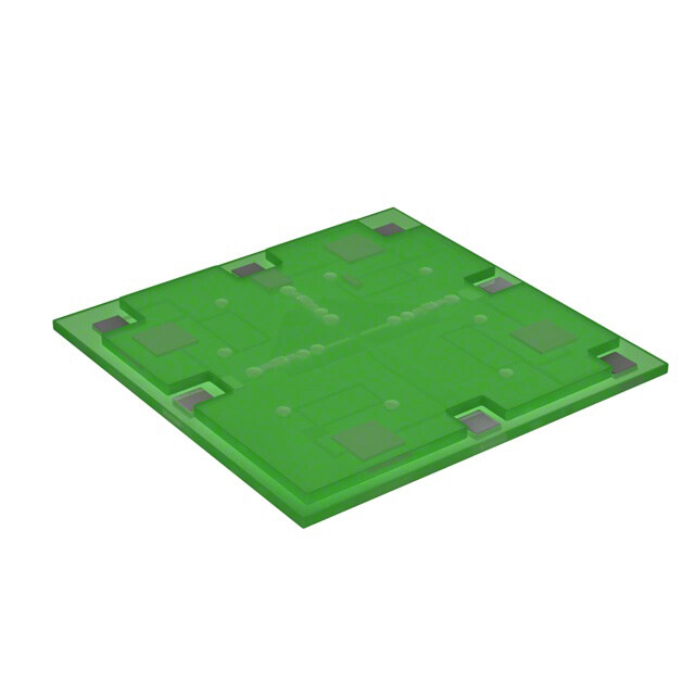
ADG901/ADG902 Data Sheet ADG901/ADG902 EVALUATION BOARD The ADG901/ADG902 evaluation board allows designers to evaluate the high performance wideband switches with a minimum of effort. To prove that these devices meet user requirements, the user requires only a power supply and a network analyzer along with the evaluation board. An application note is available with the evaluation board and provides complete information on operating the evaluation board. The RF1 port (see Figure 24) is connected through a 50 Ω transmission line to the top left SMA Connector J1. RF2 is connected through a 50 Ω transmission line to the top SMA Connector J2. J3 is connected to GND. A through transmission line connects J4 and J5 and this transmission line is used to estimate the loss of the PCB over the environmental conditions being evaluated. The board is constructed of a 4-layer, FR4 material with a dTiweloe cgtrroicu cnodn slataynetr so fw 4i.t3h agnrdo uann doevder pallal ntheisc kpnroesvsi doef 0g.r0o6u2n idn cfhoers . 03336-023 the RF transmission lines. The transmission lines were designed Figure 24. ADG901/ADG902 Evaluation Board Top View using a coplanar waveguide with ground plane model using a trace width of 0.052 inches, clearance to ground plane of 0.030 inches, dielectric thickness of 0.029 inches, and a metal thickness of 0.014 inches. Rev. D | Page 12 of 13
Data Sheet ADG901/ADG902 OUTLINE DIMENSIONS 3.20 3.00 2.80 8 5 5.15 3.20 4.90 3.00 4.65 2.80 1 4 PIN 1 IDENTIFIER 0.65 BSC 0.95 15° MAX 0.85 1.10 MAX 0.75 0.80 0.15 0.40 6° 0.23 0.55 CO0P.0L50A.1N0ARICTOYMPLIANT0. 2T5O JEDEC STA0°NDARDS 0M.0O9-187-AA 0.40 10-07-2009-B Figure 25. 8-Lead Mini Small Outline Package [MSOP] (RM-8) Dimensions shown in millimeters DETAIL A 1.84 (JEDEC 95) 3.10 1.74 3.00 SQ 2.90 0.50 1.64 BSC 5 8 PIN 1 INDEX EXPOSED 1.55 AREA PAD 1.45 0.50 1.35 0.40 0.30 4 1 TOP VIEW BOTTOM VIEW PIN 1 INDICATOR AREA OPTIONS (SEE DETAIL A) 0.80 FOR PROPER CONNECTION OF 0.75 SIDE VIEW 0.05 MAX TTHHEE EPXINP COOSENDFI GPAUDR,A RTEIOFNE RA NTOD 0.70 0.02 NOM FUNCTION DESCRIPTIONS COPLANARITY SECTION OF THIS DATA SHEET. SEATING 0.30 0.08 PLANE 0.25 0.203 REF PKG-003886 0C.O20MPLIANTTOJEDEC STANDARDS MO-229-WEED-4 02-10-2017-A Figure 26. 8-Lead Lead Frame Chip Scale Package [LFCSP] 3 mm × 3 mm Body and 0.75 mm Package Height (CP-8-13) Dimensions shown in millimeters ORDERING GUIDE Model1 Temperature Range Package Description Package Option Branding ADG901BRMZ −40°C to +85°C 8-Lead Mini Small Outline Package [MSOP] RM-8 S1T ADG901BRMZ-REEL7 −40°C to +85°C 8-Lead Mini Small Outline Package [MSOP] RM-8 S1T ADG901BCPZ-500RL7 −40°C to +85°C 8-Lead Lead Frame Chip Scale Package [LFCSP] CP-8-13 S1T ADG902BRMZ −40°C to +85°C 8-Lead Mini Small Outline Package [MSOP] RM-8 S1V EVAL-ADG901EBZ ADG901 Evaluation Board EVAL-ADG902EBZ ADG902 Evaluation Board 1 Z = RoHS Compliant Part. ©2003–2017 Analog Devices, Inc. All rights reserved. Trademarks and registered trademarks are the property of their respective owners. D03336-0-11/17(D) Rev. D | Page 13 of 13
Mouser Electronics Authorized Distributor Click to View Pricing, Inventory, Delivery & Lifecycle Information: A nalog Devices Inc.: EVAL-ADG901EBZ EVAL-ADG902EBZ ADG901BRMZ ADG901BRM ADG902BRMZ ADG901BCPZ-500RL7 ADG901BRMZ-REEL7 ADG901SCPZ-EP ADG901SCPZ-EP-RL7