ICGOO在线商城 > 集成电路(IC) > 接口 - 模拟开关,多路复用器,多路分解器 > ADG713BRZ
 Datasheet下载
- 型号: ADG713BRZ
- 制造商: Analog
- 库位|库存: xxxx|xxxx
- 要求:
| 数量阶梯 | 香港交货 | 国内含税 |
| +xxxx | $xxxx | ¥xxxx |
查看当月历史价格
查看今年历史价格
ADG713BRZ产品简介:
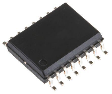
ICGOO电子元器件商城为您提供ADG713BRZ由Analog设计生产,在icgoo商城现货销售,并且可以通过原厂、代理商等渠道进行代购。 ADG713BRZ价格参考¥15.80-¥31.27。AnalogADG713BRZ封装/规格:接口 - 模拟开关,多路复用器,多路分解器, 4 Circuit IC Switch 1:1 4 Ohm 16-SOIC。您可以下载ADG713BRZ参考资料、Datasheet数据手册功能说明书,资料中有ADG713BRZ 详细功能的应用电路图电压和使用方法及教程。
ADG713BRZ是Analog Devices Inc.(ADI)生产的一款低电压、CMOS模拟开关,属于接口类的模拟开关、多路复用器和多路分解器。它具有低导通电阻(RON)、低泄漏电流和快速切换速度等特点,适用于多种应用场景。

 应用场景

1. 通信系统:
   - ADG713BRZ可以用于通信设备中的信号路由和切换。例如,在无线基站、路由器和其他网络设备中,它可以实现不同信道之间的快速切换,确保信号传输的高效性和稳定性。
   - 在多通道通信系统中,ADG713BRZ可以用作多路复用器或多路分解器,将多个输入信号合并到一个输出通道,或者将一个输入信号分配到多个输出通道。

2. 音频处理:
   - 在音频设备中,如调音台、耳机放大器和音响系统,ADG713BRZ可以用于选择不同的音频源或控制音频信号的路径。它的低导通电阻和低失真特性确保了音频信号的质量不会受到明显的影响。
   - 它还可以用于音频信号的动态路由,根据用户需求或系统状态自动切换不同的音频输入或输出端口。

3. 传感器接口:
   - 在工业自动化和物联网(IoT)应用中,ADG713BRZ可以用于连接多个传感器与单个处理器或控制器。通过多路复用功能,它可以依次读取多个传感器的数据,减少硬件资源的需求。
   - 例如,在环境监测系统中,ADG713BRZ可以用于选择不同的温度、湿度或气体传感器,并将数据传输给中央处理单元进行分析。

4. 医疗设备:
   - 在医疗电子设备中,如心电图机、血压计等,ADG713BRZ可以用于切换不同的生理信号采集通道。它的低泄漏电流特性有助于提高测量精度,确保患者安全。
   - 它还可以用于医疗成像设备中的信号路由,确保图像数据的准确性和实时性。

5. 消费电子产品:
   - 在智能手机、平板电脑和其他便携式设备中,ADG713BRZ可以用于管理多个外设接口,如USB、耳机插孔等。它的小尺寸和低功耗特性使其非常适合应用于对空间和能效有严格要求的便携式设备。

总之,ADG713BRZ凭借其优异的性能和广泛的适用性,成为许多领域中信号切换和路由的理想选择。
| 参数 | 数值 |
| 产品目录 | 集成电路 (IC)半导体 |
| 描述 | IC SWITCH QUAD SPST 16SOIC模拟开关 IC 2.5 Ohm 5.5V CMOS Quad SPST |
| 产品分类 | |
| 品牌 | Analog Devices |
| 产品手册 | |
| 产品图片 |
|
| rohs | 符合RoHS无铅 / 符合限制有害物质指令(RoHS)规范要求 |
| 产品系列 | 开关 IC,模拟开关 IC,Analog Devices ADG713BRZ- |
| 数据手册 | |
| 产品型号 | ADG713BRZ |
| PCN组件/产地 | |
| 产品培训模块 | http://www.digikey.cn/PTM/IndividualPTM.page?site=cn&lang=zhs&ptm=16845 |
| 产品种类 | 模拟开关 IC |
| 供应商器件封装 | 16-SOIC |
| 功能 | |
| 包装 | 管件 |
| 商标 | Analog Devices |
| 安装类型 | 表面贴装 |
| 安装风格 | SMD/SMT |
| 导通电阻 | 4 欧姆 |
| 封装 | Tube |
| 封装/外壳 | 16-SOIC(0.154",3.90mm 宽) |
| 封装/箱体 | SOIC-16 |
| 工作温度 | -40°C ~ 85°C |
| 工作电源电压 | 5.5 V |
| 工厂包装数量 | 48 |
| 开关数量 | 4 |
| 开关电压—最大值 | 5.5 V |
| 开关配置 | SPDT |
| 最大功率耗散 | 5 uW |
| 最大工作温度 | + 85 C |
| 最小工作温度 | - 40 C |
| 标准包装 | 48 |
| 电压-电源,单/双 (±) | 1.8 V ~ 5.5 V |
| 电压源 | 单电源 |
| 电流-电源 | 1nA |
| 电源电压-最大 | 5.5 V |
| 电源电压-最小 | V |
| 电源电流—最大值 | 1 uA |
| 电路 | 4 x SPST - NC/NO |
| 空闲时间—最大值 | 6 ns |
| 系列 | ADG713 |
| 运行时间—最大值 | 11 ns |


- 商务部:美国ITC正式对集成电路等产品启动337调查
- 曝三星4nm工艺存在良率问题 高通将骁龙8 Gen1或转产台积电
- 太阳诱电将投资9.5亿元在常州建新厂生产MLCC 预计2023年完工
- 英特尔发布欧洲新工厂建设计划 深化IDM 2.0 战略
- 台积电先进制程称霸业界 有大客户加持明年业绩稳了
- 达到5530亿美元!SIA预计今年全球半导体销售额将创下新高
- 英特尔拟将自动驾驶子公司Mobileye上市 估值或超500亿美元
- 三星加码芯片和SET,合并消费电子和移动部门,撤换高东真等 CEO
- 三星电子宣布重大人事变动 还合并消费电子和移动部门
- 海关总署:前11个月进口集成电路产品价值2.52万亿元 增长14.8%


PDF Datasheet 数据手册内容提取
CMOS Low Voltage, 4 Ω Quad, SPST Switches ADG711/ADG712/ADG713 FEATURES FUNCTIONAL BLOCK DIAGRAM 1.8 V to 5.5 V single supply S1 S1 S1 Low on resistance (2.5 Ω Typ) IN1 IN1 IN1 D1 D1 D1 Low on resistance flatness S2 S2 S2 −3 dB bandwidth > 200 MHz IN2 IN2 IN2 Rail-to-rail operation D2 D2 D2 ADG711 ADG712 ADG713 16-lead TSSOP and SOIC packages S3 S3 S3 Fast switching times: t =16 ns, t =10 ns IN3 IN3 IN3 ON OFF D3 D3 D3 Typical power consumption (< 0.01 μW) S4 S4 S4 TTL/CMOS compatible IN4 IN4 IN4 Qualified for automotive applications D4 D4 D4 APPLICATIONS SWITCHES SHOWN FOR A LOGIC “1” INPUT 00042-001 Figure 1. USB 1.1 signal switching circuits Cell phones PDAs Battery-powered systems Communication systems Sample hold systems Audio signal routing Video switching Mechanical reed relay replacement GENERAL DESCRIPTION The ADG711, ADG712, and ADG713 are monolithic CMOS The ADG711/ADG712/ADG713 are available in 16-lead TSSOP devices containing four independently selectable switches. These and 16-lead SOIC packages. switches are designed on an advanced submicron process that PRODUCT HIGHLIGHTS provides low power dissipation yet gives high switching speed, low on resistance, low leakage currents, and high bandwidth. 1. 1.8 V to 5.5 V Single-Supply Operation. The ADG711, ADG712, and ADG713 offer high performance They are designed to operate from a single 1.8 V to 5.5 V supply, and are fully specified and guaranteed with 3 V and 5 V making them ideal for use in battery-powered instruments and supply rails. with the new generation of DACs and ADCs from Analog Devices, Inc. Fast switching times and high bandwidth make the parts 2. Very Low RON (4.5 Ω maximum at 5 V, 8 Ω maximum at 3 V). suitable for switching USB 1.1 data signals and video signals. At supply voltage of 1.8 V, RON is typically 35 Ω over the temperature range. The ADG711, ADG712, and ADG713 contain four independent single-pole/single-throw (SPST) switches. The ADG711 and 3. Low On Resistance Flatness. ADG712 differ only in that the digital control logic is inverted. The 4. −3 dB Bandwidth >200 MHz. ADG711 switches are turned on with a logic low on the appropriate 5. Low Power Dissipation. CMOS construction ensures low control input, while a logic high is required to turn on the switches power dissipation. of the ADG712. The ADG713 contains two switches whose digital control logic is similar to the ADG711, while the logic is inverted 6. Fast tON/tOFF. on the other two switches. 7. Break-Before-Make Switching. Each switch conducts equally well in both directions when On. The This prevents channel shorting when the switches are ADG713 exhibits break-before-make switching action. configured as a multiplexer (ADG713 only). 8. 16-Lead TSSOP and 16-Lead SOIC Packages. Rev. B Information furnished by Analog Devices is believed to be accurate and reliable. However, no responsibility is assumed by Analog Devices for its use, nor for any infringements of patents or other One Technology Way, P.O. Box 9106, Norwood, MA 02062-9106, U.S.A. rights of third parties that may result from its use. Specifications subject to change without notice. No license is granted by implication or otherwise under any patent or patent rights of Analog Devices. Tel: 781.329.4700 www.analog.com Trademarks and registered trademarks are the property of their respective owners. Fax: 781.461.3113 ©2004–2011 Analog Devices, Inc. All rights reserved.
ADG711/ADG712/ADG713 TABLE OF CONTENTS Features..............................................................................................1 Pin Configuration and Function Descriptions..............................6 Applications.......................................................................................1 Typical Performance Characteristics..............................................7 Functional Block Diagram..............................................................1 Test Circuits........................................................................................9 General Description.........................................................................1 Terminology....................................................................................11 Product Highlights...........................................................................1 Applications Information..............................................................12 Revision History...............................................................................2 Outline Dimensions.......................................................................13 Specifications.....................................................................................3 Ordering Guide..........................................................................14 Absolute Maximum Ratings............................................................5 Automotive Products.................................................................14 ESD Caution..................................................................................5 REVISION HISTORY 6/11—Rev. A to Rev. B Updated Format..................................................................Universal Changes to Features Section............................................................1 Changes to Absolute Maximum Ratings Table.............................5 Changes to Ordering Guide..........................................................14 Added Automotive Products Section..........................................14 3/04—Rev. 0 to Rev. A Added Applications..........................................................................1 Changes to Ordering Guide............................................................4 Updated Outline Dimensions.......................................................10 Rev. B | Page 2 of 16
ADG711/ADG712/ADG713 SPECIFICATIONS V = +5 V ± 10%, GND = 0 V. All specifications −40°C to +85°C, unless otherwise noted. DD Table 1. Parameter +25°C −40°C to +85°C Unit Test Conditions/Comments ANALOG SWITCH Analog Signal Range 0 V to V V DD On Resistance (R ) 2.5 Ω typ V = 0 V to V , I = −10 mA; ON S DD S 4 4.5 Ω max See Figure 11 On Resistance Match Between 0.05 Ω typ V = 0 V to V , I = −10 mA S DD S Channels (ΔR ) 0.3 Ω max ON On Resistance Flatness (R ) 0.5 Ω typ V = 0 V to V , I = −10 mA FLAT(ON) S DD S 1.0 Ω max LEAKAGE CURRENTS V = +5.5 V DD Source Off Leakage I (Off) ±0.01 nA typ V = 4.5 V/1 V, V = 1 V/4.5 V S S D ±0.1 ±0.2 nA max See Figure 12 Drain Off Leakage I (Off) ±0.01 nA typ V = 4.5 V/1 V, V = 1 V/4.5 V D S D ±0.1 ±0.2 nA max See Figure 12 Channel On Leakage I , I (On) ±0.01 nA typ V = V = 1 V, or 4.5 V D S S D ±0.1 ±0.2 nA max See Figure 13 DIGITAL INPUTS Input High Voltage, V 2.4 V min INH Input Low Voltage, V 0.8 V max INL Input Current I or I 0.005 μA typ V = V or V INL INH IN INL INH ±0.1 μA max DYNAMIC CHARACTERISTICS1 t 11 ns typ R = 300 Ω, C = 35 pF ON L L 16 ns max V = 3 V; see Figure 14 S t 6 ns typ R = 300 Ω, C = 35 pF OFF L L 10 ns max V = 3 V; see Figure 14 S Break-Before-Make Time Delay, t 6 ns typ R = 300 Ω, C = 35 pF D L L (ADG713 Only) 1 ns min V = V = 3 V; see Figure 15 S1 S2 Charge Injection 3 pC typ V = 2 V; R = 0 Ω, C = 1 nF; see Figure 16 S S L Off Isolation −58 dB typ R = 50 Ω, C = 5 pF, f = 10 MHz L L −78 dB typ R = 50 Ω, C = 5 pF, f = 1 MHz; see Figure 17 L L Channel-to-Channel Crosstalk −90 dB typ R = 50 Ω, C = 5 pF, f = 10 MHz; see Figure 18 L L Bandwidth −3 dB 200 MHz typ R = 50 Ω, C = 5 pF; see Figure 19 L L C 10 pF typ S C 10 pF typ D C , C (On) 22 pF typ D S POWER REQUIREMENTS V = +5.5 V DD I 0.001 μA typ Digital inputs = 0 V or 5 V DD 1.0 μ max 1 Guaranteed by design, not subject to production test. Rev. B | Page 3 of 16
ADG711/ADG712/ADG713 V = +3 V ± 10%, GND = 0 V. All specifications −40°C to +85°C, unless otherwise noted. DD Table 2. Parameter +25°C −40°C to +85°C Unit Test Conditions/Comments ANALOG SWITCH Analog Signal Range 0 V to V V DD On Resistance (R ) 5 5.5 Ω typ V = 0 V to V , I = −10 mA; ON S DD S 8 Ω max See Figure 11 On Resistance Match Between 0.1 Ω typ V = 0 V to V , I = −10 mA S DD S Channels (ΔR ) 0.3 Ω max ON On Resistance Flatness (R ) 2.5 Ω typ V = 0 V to V , I = −10 mA FLAT(ON) S DD S LEAKAGE CURRENTS V = +3.3 V DD Source Off Leakage I (Off) ±0.01 nA typ V = 3 V/1 V, V = 1 V/3 V S S D ±0.1 ±0.2 nA max See Figure 12 Drain Off Leakage I (Off) ±0.01 nA typ V = 3 V/1 V, V = 1 V/ 3 V D S D ±0.1 ±0.2 nA max See Figure 12 Channel On Leakage I , I (On) ±0.01 nA typ V = V = 1 V, or 3 V D S S D ±0.1 ±0.2 nA max See Figure 13 DIGITAL INPUTS Input High Voltage, V 2.0 V min INH Input Low Voltage, V 0.4 V max INL Input Current I or I 0.005 μA typ V = V or V INL INH IN INL INH ±0.1 μA max DYNAMIC CHARACTERISTICS1 t 13 ns typ R = 300 Ω, C = 35 pF ON L L 20 ns max V = 2 V; see Figure 14 S t 7 ns typ R = 300 Ω, C = 35 pF OFF L L 12 ns max V = 2 V; see Figure 14 S Break-Before-Make Time Delay, t 7 ns typ R = 300 Ω, C = 35 pF D L L (ADG713 Only) 1 ns min V = V = 2 V; see Figure 15 S1 S2 Charge Injection 3 pC typ V = 1.5 V; R = 0 Ω, C = 1 nF; see Figure 16 S S L Off Isolation −58 dB typ R = 50 Ω, C = 5 pF, f = 10 MHz L L −78 dB typ R = 50 Ω, C = 5 pF, f = 1 MHz; see Figure 17 L L Channel-to-Channel Crosstalk −90 dB typ R = 50 Ω, C = 5 pF, f = 10 MHz; see Figure 18 L L Bandwidth −3 dB 200 MHz typ R = 50 Ω, C = 5 pF; see Figure 19 L L C 10 pF typ S C 10 pF typ D C , C (On) 22 pF typ D S POWER REQUIREMENTS V = +3.3 V DD I 0.001 μA typ Digital inputs = 0 V or 3 V DD 1.0 μ max 1 Guaranteed by design, not subject to production test. Rev. B | Page 4 of 16
ADG711/ADG712/ADG713 ABSOLUTE MAXIMUM RATINGS T = +25°C, unless otherwise noted. Stresses above those listed under Absolute Maximum Ratings A may cause permanent damage to the device. This is a stress Table 3. rating only; functional operation of the device at these or any Parameter Rating other conditions above those indicated in the operational VDD to GND −0.3 V to +6 V section of this specification is not implied. Exposure to absolute Analog, Digital Inputs1 −0.3 V to VDD +0.3 V or maximum rating conditions for extended periods may affect 30 mA, whichever occurs device reliability. first Continuous Current, S or D 30 mA Only one absolute maximum rating may be applied at any Peak Current, S or D 100 mA (Pulsed at 1 ms, one time. 10% duty cycle maximum) ESD CAUTION Operating Temperature Range −40°C to +85°C Storage Temperature Range −65°C to +150°C Junction Temperature 150°C TSSOP Package, Power Dissipation 430 mW θJA Thermal Impedance 150°C/W θJC Thermal Impedance 27°C/W SOIC Package, Power Dissipation 520 mW θ Thermal Impedance 125°C/W JA θ Thermal Impedance 42°C/W JC Lead Temperature, Soldering Vapor Phase (60 sec) 215°C Infrared (15 sec) 220°C Soldering(Pb-Free) Reflow, Peak Temperature 260(+0/−5)°C Time at Peak Temperature 20 sec to 40 sec ESD 2 kV 1 Overvoltages at IN, S or D will be clamped by internal diodes. Currents should be limited to the maximum ratings given. Rev. B | Page 5 of 16
ADG711/ADG712/ADG713 PIN CONFIGURATION AND FUNCTION DESCRIPTIONS IN1 1 16 IN2 D1 2 ADG711/ 15 D2 S1 3 ADG712/ 14 S2 NC 4 ADG713 13 VDD GND 5 12 NC S4 6 TOP VIEW 11 S3 D4 7 (Not to Scale) 10 D3 IN4 8 9 IN3 N1.O CNTOCE NS=N NEOC TCOTON NTEHCIST .P DINO. NOT 00042-004 Figure 2. Pin Configuration Table 4. Pin Number Mnemonic Description 1 IN1 Digital Control Input. Its logic state controls the status of the Switch S1-D1. 2 D1 Drain Pin. Can be used as input or output. 3 S1 Source Pin. Can be used as input or output. 4 NC Not internally connected. 5 GND The most negative power supply pin. 6 S4 Source Pin. Can be used as input or output. 7 D4 Drain Pin. Can be used as input or output. 8 IN4 Digital Control Input. Its logic state controls the status of the Switch S4-D4. 9 IN3 Digital Control Input. Its logic state controls the status of the Switch S3-D3. 10 D3 Drain Pin. Can be used as input or output. 11 S3 Source Pin. Can be used as input or output. 12 NC Not internally connected. 13 V The most positive power supply pin. DD 14 S2 Source Pin. Can be used as input or output. 15 D2 Drain Pin. Can be used as input or output. 16 IN2 Digital Control Input. Its logic state controls the status of the Switch S3-D3. Table 5. Truth Table (ADG711/ADG712) ADG711 In ADG712 In Switch Condition 0 1 On 1 0 Off Table 6. Truth Table (ADG713) Logic Switch 1, 4 Switch 2, 3 0 Off On 1 On Off Rev. B | Page 6 of 16
ADG711/ADG712/ADG713 TYPICAL PERFORMANCE CHARACTERISTICS 6.0 10m VDD = 5V 5.5 TA = 25°C 1m 5.0 VDD = 2.7V 4.5 100µ 4.0 4 SW (Ω)ON 33..50 VDD = 3.0V VDD = 4.5V (A)PLY 10µ 8 SW R 2.5 UP 1µ S I 2.0 VDD = 5.0V 100n 1.5 1.0 10n 0.5 00 0.5 1.0DR1A.I5N OR2. 0SOU2R.C5E V3O.0LTAG3E.5 (V)4.0 4.5 5.0 00042-005 1n100 1k F1R0EkQUENCY1 (0H0zk) 1M 10M 00042-008 Figure 3. On Resistance as a Function of VD (VS) Figure 6. Supply Current vs. Input Switching Frequency 6.0 –30 5.5 VDD = 3V –40 VDD = 5V, 3V 5.0 TA = +85°C –50 4.5 TA = +25°C 4.0 dB) –60 R (Ω)ON 332...505 F ISOLATION ( –––789000 2.0 TA = –40°C OF–100 1.5 –110 1.0 –120 0.5 00 0.5 DRAI1N. 0OR SOU1R.C5E VOLTA2.G0E (V) 2.5 3.0 00042-006 –13010k 100k FREQU1EMNCY (Hz) 10M 100M 00042-009 Figure 4. On Resistance as a Function of VD (VS) for Different Temperatures Figure 7. Off Isolation vs. Frequency VDD = 3 V 6.0 –30 5.5 VDD = 5V –40 VDD = 5V, 3V 5.0 –50 4.5 –60 Ω) 43..05 TA = +85°C K (dB) –70 (N 3.0 TA = +25°C AL –80 O T R 2.5 OS –90 R 2.0 C –100 1.5 TA = –40°C –110 1.0 –120 0.5 00 0.5 1.0DR1A.I5N OR2. 0SOU2R.C5E V3O.0LTAG3E.5 (V)4.0 4.5 5.0 00042-007 –13010k 100k FREQU1EMNCY (Hz) 10M 100M 00042-010 Figure 5. On Resistance as a Function of VD (VS) for Different Temperatures Figure 8. Crosstalk vs. Frequency VDD = 5 V Rev. B | Page 7 of 16
ADG711/ADG712/ADG713 0 25 TA = 25°C VDD = 5V 20 15 B) –2 SE (d C) 10 VDD = 5V ESPON Q (pINJ 5 VDD = 3V R N –4 O 0 –5 –610k 100k FREQ1MUENCY (Hz)10M 100M 00042-011 –100 0.5 1.0 1.5SOU2R.0CE V2O.5LTA3G.0E (V)3.5 4.0 4.5 5.0 00042-012 Figure 9. On Response vs. Frequency Figure 10. Charge Injection vs. Source Voltage Rev. B | Page 8 of 16
ADG711/ADG712/ADG713 TEST CIRCUITS IDS V1 S D ID (AON) S D VS VD 00042-015 VS RON = V1/IDS 00042-013 Figure 13. On Leakage Figure 11. On Resistance IS (OFF) S D ID (OFF) A A VS VD 00042-014 Figure 12. Off Leakage VDD 0.1µF VIN ADG711 50% 50% VDD VIN ADG712 50% 50% S D VOUT VS IN R30L0Ω C35LpF VOUT VS 90% 90% GND tON tOFF 00042-016 Figure 14. Switching Times VDD 0.1µF VIN 50% 50% 0V VDD 90% 90% S1 D1 VOUT1 VS1 VOUT1 0V VS2 S2 D2 VOUT2 R30L01Ω C35Lp1F IN1, IN2 R30L02Ω C35Lp2F VOUT2 90% 90% ADGGND713 0V tD tD 00042-017 Figure 15. Break-Before-Make Time Delay, tD VDD SW ON SW OFF VDD VIN RS S D VOUT VS IN C15LnF VOUT ∆VOUT GND QINJ = CL × VOUT 00042-018 Figure 16. Charge Injection
ADG711/ADG712/ADG713 VDD VDD 0.1µF 0.1µF VDD VDD S D S D VOUT VOUT RL RL 50Ω 50Ω VS VIN IN VS VIN IN GND 00042-019 GND 00042-021 Figure 17. Off Isolation Figure 19. Bandwidth VDD 0.1µF VDD S D 50Ω VS VIN1 VIN2 S D NC VOUT RL 50Ω GND CHANNEL-TO-CHANNEL CROSSTALK = 20 × log |VS/VOUT| 00042-020 Figure 18. Channel-to-Channel Crosstalk Rev. B | Page 10 of 16
ADG711/ADG712/ADG713 TERMINOLOGY t R ON ON Delay between applying the digital control input and the output Ohmic resistance between D and S. switching on. ΔR ON t On resistance match between any two channels, ie., R max − OFF ON Delay between applying the digital control input and the output R min. ON switching off. R FLAT(ON) t Flatness is defined as the difference between the maximum and D Off time or on time measured between the 90% points of both minimum value of on resistance as measured over the specified switches, when switching from one address state to another analog signal range. (ADG713 only). I (OFF) S Crosstalk Source leakage current with the switch off. A measure of unwanted signal that is coupled through from one I (OFF) D channel to another as a result of parasitic capacitance. Drain leakage current with the switch off. Off Isolation I , I (ON) D S A measure of unwanted signal coupling through an off switch. Channel leakage current with the switch on. Charge Injection V (V) D S A measure of the glitch impulse transferred from the digital Analog voltage on Terminals D, S. input to the analog output during switching. C (OFF) S Bandwidth Off switch source capacitance. The frequency at which the output is attenuated by 3 dB. C (OFF) On Response D Off switch drain capacitance. The frequency response of the on switch. C , C (ON) D S On switch capacitance.
ADG711/ADG712/ADG713 APPLICATIONS INFORMATION Figure 20 illustrates a photodetector circuit with programmable C1 gain. An AD820 is used as the output operational amplifier. R1 With the resistor values shown in the circuit, and using different 33kΩ +5V combinations of the switches, gain in the range of 2 to 16 can be AD820 achieved. D1 +2.5V VOUT R2 510kΩ +5V R4 R5 S1 D1 240kΩ 240kΩ (LSB) IN1 R6 R7 R3 S2 D2 120kΩ 120kΩ 510kΩ IN2 R8 S3 D3 120kΩ IN3 R9 S4 D4 120kΩ +2.5V (MSB) IN4 R10 GND 120kΩ 00042-022 Figure 20. Photodetector Circuit with Programmable Gain Rev. B | Page 12 of 16
ADG711/ADG712/ADG713 OUTLINE DIMENSIONS 10.00 (0.3937) 9.80 (0.3858) 4.00 (0.1575) 16 9 6.20 (0.2441) 3.80 (0.1496) 1 8 5.80 (0.2283) 1.27 (0.0500) 0.50 (0.0197) BSC 45° 1.75 (0.0689) 0.25 (0.0098) 0.25 (0.0098) 1.35 (0.0531) 8° 0.10 (0.0039) 0° COPLANARITY SEATING 0.10 0.51 (0.0201) PLANE 0.25 (0.0098) 1.27 (0.0500) 0.31 (0.0122) 0.17 (0.0067) 0.40 (0.0157) COMPLIANTTO JEDEC STANDARDS MS-012-AC C(RINOEFNPEATRRREOENNLCLTEIHN EOGSN EDLSIYM)AEANNRDSEI AORRNOESU NANORDEET DAIN-PO MPFRIFLO LMPIIMRLELIATIMTEEER TFSEO; RIRN ECUQHSU EDI VIINMA LEDENENSSTIIOGSN NFS.OR 060606-A Figure 21. 16-Lead Standard Small Outline Package [SOIC] Narrow Body (R-16) Dimensions shown in millimeters and (inches) 5.10 5.00 4.90 16 9 4.50 6.40 4.40 BSC 4.30 1 8 PIN 1 1.20 MAX 0.15 0.20 0.05 0.09 0.75 0.30 8° 0.60 B0S.6C5 0.19 SEATING 0° 0.45 PLANE COPLANARITY 0.10 COMPLIANT TO JEDEC STANDARDS MO-153-AB Figure 22. 16-Lead Thin Shrink Small Outline Package [TSSOP] (RU-16) Dimensions shown in millimeters Rev. B | Page 13 of 16
ADG711/ADG712/ADG713 ORDERING GUIDE Model1, 2 Temperature range Package Description Package Option ADG711BR −40°C to +85°C Standard Small Outline(SOIC) R-16 ADG711BR-REEL −40°C to +85°C Standard Small Outline(SOIC) R-16 ADG711BR-REEL7 −40°C to +85°C Standard Small Outline(SOIC) R-16 ADG711BRZ −40°C to +85°C Standard Small Outline(SOIC) R-16 ADG711BRZ-REEL −40°C to +85°C Standard Small Outline(SOIC) R-16 ADG711BRZ-REEL7 −40°C to +85°C Standard Small Outline(SOIC) R-16 ADG711BRU −40°C to +85°C Thin Shrink Small Outline(TSSOP) RU-16 ADG711BRU-REEL −40°C to +85°C Thin Shrink Small Outline(TSSOP) RU-16 ADG711BRU-REEL7 −40°C to +85°C Thin Shrink Small Outline(TSSOP) RU-16 ADG711BRUZ −40°C to +85°C Thin Shrink Small Outline(TSSOP) RU-16 ADG711BRUZ-REEL −40°C to +85°C Thin Shrink Small Outline(TSSOP) RU-16 ADG711BRUZ-REEL7 −40°C to +85°C Thin Shrink Small Outline(TSSOP) RU-16 ADG711WBRUZ-REEL −40°C to +85°C Thin Shrink Small Outline(TSSOP) RU-16 ADG712BR −40°C to +85°C Standard Small Outline(SOIC) R-16 ADG712BR-REEL −40°C to +85°C Standard Small Outline(SOIC) R-16 ADG712BR-REEL7 −40°C to +85°C Standard Small Outline(SOIC) R-16 ADG712BRZ −40°C to +85°C Standard Small Outline(SOIC) R-16 ADG712BRZ-REEL −40°C to +85°C Standard Small Outline(SOIC) R-16 ADG712BRZ-REEL7 −40°C to +85°C Standard Small Outline(SOIC) R-16 ADG712BRU −40°C to +85°C Thin Shrink Small Outline(TSSOP) RU-16 ADG712BRU-REEL −40°C to +85°C Thin Shrink Small Outline(TSSOP) RU-16 ADG712BRU-REEL7 −40°C to +85°C Thin Shrink Small Outline(TSSOP) RU-16 ADG712BRUZ −40°C to +85°C Thin Shrink Small Outline(TSSOP) RU-16 ADG712BRUZ-REEL −40°C to +85°C Thin Shrink Small Outline(TSSOP) RU-16 ADG712BRUZ-REEL7 −40°C to +85°C Thin Shrink Small Outline(TSSOP) RU-16 ADG713BR −40°C to +85°C Standard Small Outline(SOIC) R-16 ADG713BRZ −40°C to +85°C Standard Small Outline(SOIC) R-16 ADG713BRZ-REEL −40°C to +85°C Standard Small Outline(SOIC) R-16 ADG713BRZ-REEL7 −40°C to +85°C Standard Small Outline(SOIC) R-16 ADG713BRU −40°C to +85°C Thin Shrink Small Outline(TSSOP) RU-16 ADG713BRU-REEL −40°C to +85°C Thin Shrink Small Outline(TSSOP) RU-16 ADG713BRU-REEL7 −40°C to +85°C Thin Shrink Small Outline(TSSOP) RU-16 ADG713BRUZ −40°C to +85°C Thin Shrink Small Outline(TSSOP) RU-16 ADG713BRUZ-REEL −40°C to +85°C Thin Shrink Small Outline(TSSOP) RU-16 ADG713BRUZ-REEL7 −40°C to +85°C Thin Shrink Small Outline(TSSOP) RU-16 1 Z = RoHS Compliant Part. 2 W = Qualified for Automotive Applications. AUTOMOTIVE PRODUCTS The AD711W models are available with controlled manufacturing to support the quality and reliability requirements of automotive applications. Note that these automotive models may have specifications that differ from the commercial models; therefore, designers should review the Specifications section of this data sheet carefully. Only the automotive grade products shown are available for use in automotive applications. Contact your local Analog Devices account representative for specific product ordering information and to obtain the specific Automotive Reliability reports for these models. Rev. B | Page 14 of 16
ADG711/ADG712/ADG713 NOTES Rev. B | Page 15 of 16
ADG711/ADG712/ADG713 NOTES ©2004–2011 Analog Devices, Inc. All rights reserved. Trademarks and registered trademarks are the property of their respective owners. D00042-0-6/11(B) Rev. B | Page 16 of 16
Mouser Electronics Authorized Distributor Click to View Pricing, Inventory, Delivery & Lifecycle Information: A nalog Devices Inc.: ADG713BR-REEL ADG711BR-REEL7 ADG711WBRUZ-REEL ADG712BRU-REEL7 ADG713BRUZ-REEL7 ADG712BRUZ ADG712BRZ ADG713BRUZ ADG711BRUZ ADG713BRZ ADG712BRUZ-REEL7 ADG711BRZ ADG713BRZ-REEL7 ADG712BRUZ-REEL ADG713BRUZ-REEL ADG713BRZ-REEL ADG711BRUZ-REEL ADG711BRZ-REEL ADG712BRZ-REEL7 ADG711BRZ-REEL7 ADG711BRUZ-REEL7 ADG711BRU ADG711BR ADG712BRU