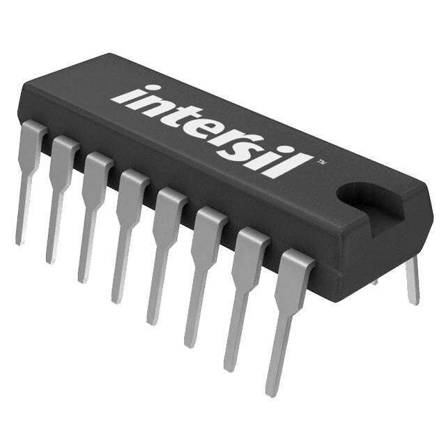
ICGOO在线商城 > 集成电路(IC) > 接口 - 模拟开关,多路复用器,多路分解器 > ADG608BRZ-REEL
- 型号: ADG608BRZ-REEL
- 制造商: Analog
- 库位|库存: xxxx|xxxx
- 要求:
| 数量阶梯 | 香港交货 | 国内含税 |
| +xxxx | $xxxx | ¥xxxx |
查看当月历史价格
查看今年历史价格
ADG608BRZ-REEL产品简介:
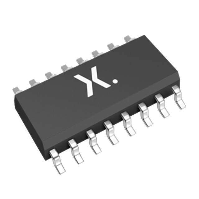
ICGOO电子元器件商城为您提供ADG608BRZ-REEL由Analog设计生产,在icgoo商城现货销售,并且可以通过原厂、代理商等渠道进行代购。 ADG608BRZ-REEL价格参考。AnalogADG608BRZ-REEL封装/规格:接口 - 模拟开关,多路复用器,多路分解器, 1 Circuit IC Switch 8:1 30Ohm 16-SOIC。您可以下载ADG608BRZ-REEL参考资料、Datasheet数据手册功能说明书,资料中有ADG608BRZ-REEL 详细功能的应用电路图电压和使用方法及教程。
| 参数 | 数值 |
| 产品目录 | 集成电路 (IC) |
| 描述 | IC MULTIPLEXER 8X1 16SOIC |
| 产品分类 | |
| 品牌 | Analog Devices Inc |
| 数据手册 | |
| 产品图片 |
|
| 产品型号 | ADG608BRZ-REEL |
| PCN组件/产地 | |
| rohs | 无铅 / 符合限制有害物质指令(RoHS)规范要求 |
| 产品系列 | - |
| 产品培训模块 | http://www.digikey.cn/PTM/IndividualPTM.page?site=cn&lang=zhs&ptm=16845 |
| 供应商器件封装 | 16-SOIC |
| 其它名称 | ADG608BRZ-REELCT |
| 功能 | 多路复用器 |
| 包装 | 剪切带 (CT) |
| 安装类型 | 表面贴装 |
| 导通电阻 | 50 欧姆 |
| 封装/外壳 | 16-SOIC(0.154",3.90mm 宽) |
| 工作温度 | -40°C ~ 85°C |
| 标准包装 | 1 |
| 电压-电源,单/双 (±) | 3V, 5V, ±5V |
| 电压源 | 单/双电源 |
| 电流-电源 | 50nA |
| 电路 | 1 x 8:1 |



- 商务部:美国ITC正式对集成电路等产品启动337调查
- 曝三星4nm工艺存在良率问题 高通将骁龙8 Gen1或转产台积电
- 太阳诱电将投资9.5亿元在常州建新厂生产MLCC 预计2023年完工
- 英特尔发布欧洲新工厂建设计划 深化IDM 2.0 战略
- 台积电先进制程称霸业界 有大客户加持明年业绩稳了
- 达到5530亿美元!SIA预计今年全球半导体销售额将创下新高
- 英特尔拟将自动驾驶子公司Mobileye上市 估值或超500亿美元
- 三星加码芯片和SET,合并消费电子和移动部门,撤换高东真等 CEO
- 三星电子宣布重大人事变动 还合并消费电子和移动部门
- 海关总署:前11个月进口集成电路产品价值2.52万亿元 增长14.8%


PDF Datasheet 数据手册内容提取
a 3 V/5 V, 4/8 Channel High Performance Analog Multiplexers ADG608/ADG609 FEATURES FUNCTIONAL BLOCK DIAGRAMS +3 V, +5 V, (cid:54)5 V Power Supplies V to V Analog Signal Range ADG608 ADG609 SS DD Low On Resistance (30 (cid:86) max) S1 S1A Fast Switching Times DA tON 75 ns max S4A t 45 ns max OFF Low Power Dissipation (1.5 (cid:109)W max) D Break-Before-Make Construction S1B ESD > 5000 V as per Military Standard 3015.7 DB TTL and CMOS Compatible Inputs S8 S4B APPLICATIONS 1 OF 8 1 OF 4 DECODER DECODER Automatic Test Equipment Data Acquisition Systems Communication Systems A0A1A2EN A0A1EN Avionics and Military Systems Microprocessor Controlled Analog Systems Medical Instrumentation The ability to operate from single +3 V, +5 V or – 5 V bipolar Battery Powered Instruments supplies makes the ADG608 and ADG609 perfect for use in Remote Powered Equipment battery operated instruments and with the new generation of Compatible with (cid:54)5 V DACs and ADCs such as DACs and ADCs from Analog Devices. The use of 5 V sup- AD7840/8, AD7870/1/2/4/5/6/8 plies and reduced operating currents gives much lower power dissipation than devices operating from – 15 V supplies. GENERAL DESCRIPTION The ADG608 and ADG609 are monolithic CMOS analog mul- PRODUCT HIGHLIGHTS tiplexers comprising eight single channels and four differential 1. Extended Signal Range channels respectively, fully specified for – 5 V, +5 V and +3 V The ADG608/ADG609 are fabricated on an enhanced power supplies. The ADG608 switches one of eight inputs to a LC2MOS process giving an increased signal range which common output as determined by the 3-bit binary address lines extends to the supplies. A0, A1 and A2. The ADG609 switches one of four differential 2. Low Power Dissipation inputs to a common differential output as determined by the 2-bit binary address lines A0 and A1. An EN input on both de- 3. Low R ON vices is used to enable or disable the device. When disabled, all 4. Fast Switching Times channels are switched OFF. All the address and enable inputs 5. Break-Before-Make Switching are TTL compatible over the full specified operating tempera- Switches are guaranteed break-before-make so that input ture range, making the parts suitable for bus-controlled systems signals are protected against momentary shorting. such as data acquisition systems, process controls, avionics and ATEs since the TTL compatible address inputs simplify the digital 6. Single/Dual Supply Operation interface design and reduce the board space requirements. The ADG608/ADG609 are designed on an enhanced LC2MOS ORDERING GUIDE process that provides low power dissipation yet gives high Model Temperature Range Package Option* switching speed and low on resistance. Each channel conducts equally well in both directions when ON and has an input signal ADG608BN –40(cid:176) C to +85(cid:176) C N-16 range which extends to the supplies. In the OFF condition, sig- ADG608BR –40(cid:176) C to +85(cid:176) C R-16A nal levels up to the supplies are blocked. All channels exhibit ADG608BRU –40(cid:176) C to +85(cid:176) C RU-16 break-before-make switching action preventing momentary ADG608TRU –55(cid:176) C to +125(cid:176) C RU-16 shorting when switching channels. Inherent in the design is low ADG609BN –40(cid:176) C to +85(cid:176) C N-16 charge injection for minimum transients when switching the ADG609BR –40(cid:176) C to +85(cid:176) C R-16A digital inputs. ADG609BRU –40(cid:176) C to +85(cid:176) C RU-16 *N = Plastic DIP; RU = Thin Shrink Small Outline Package (TSSOP); REV.A R = 0.15" Small Outline IC (SOIC). Information furnished by Analog Devices is believed to be accurate and © Analog Devices, Inc., 1995 reliable. However, no responsibility is assumed by Analog Devices for its use, nor for any infringements of patents or other rights of third parties which may result from its use. No license is granted by implication or One Technology Way, P.O. Box 9106, Norwood, MA 02062-9106, U.S.A. otherwise under any patent or patent rights of Analog Devices. Tel: 617/329-4700 Fax: 617/326-8703
ADG608/ADG609–SPECIFICATIONS DUAL SUPPLY1 (V = +5 V (cid:54) 10%, V = –5 V (cid:54) 10%, GND = 0 V, unless otherwise noted) DD SS Parameter B Version T Version +25(cid:56)C –40(cid:176) C to +25(cid:56)C –55(cid:56)C to Test Conditions/ +85(cid:56)C +125(cid:56)C Units Comments ANALOG SWITCH Analog Signal Range V to V V to V V SS DD SS DD R 22 22 W typ –3.5 V < V < +3.5 V, I = –1 mA; ON S S 30 35 30 40 W max V = +4.5 V, V = –4.5 V; DD SS Test Circuit 1 D R 5 6 5 6 W max –3 V < V < +3 V, I = –1 mA; ON S DS V = +5 V, V = –5 V DD SS R Match 2 3 2 3 W max V = 0 V, I = –1 mA; ON S DS V = +5 V, V = –5 V DD SS LEAKAGE CURRENTS V = +5.5 V, V = –5.5 V DD SS Source OFF Leakage I (OFF) – 0.05 – 0.05 nA typ V = – 4.5 V, V = (cid:55)4.5 V; S D S – 0.5 – 2 – 0.5 – 10 nA max Test Circuit 2 Drain OFF Leakage I (OFF) – 0.05 – 0.05 nA typ V = – 4.5 V, V = (cid:55)4.5 V; D D S ADG608 – 0.5 – 2 – 0.5 – 10 nA max Test Circuit 3 ADG609 – 0.5 – 1 – 0.5 – 5 nA max Channel ON Leakage I , I (ON) – 0.05 – 0.05 nA typ V = V = – 4.5 V; D S S D ADG608 – 0.5 – 3 – 0.5 – 20 nA max Test Circuit 4 ADG609 – 0.5 – 1.5 – 0.5 – 10 nA max DIGITAL INPUTS Input High Voltage, V 2.4 2.4 V min INH Input Low Voltage, V 0.8 0.8 V max INL Input Current I or I – 1 – 1 m A max V = 0 or V INL INH IN DD C , Digital Input Capacitance 5 5 pF typ IN DYNAMIC CHARACTERISTICS2 t 50 50 ns typ R = 300 W , C = 35 pF; TRANSITION L L 75 90 75 100 ns max V = – 3.5 V, V = (cid:55)3.5 V; S1 S8 Test Circuit 5 t 10 10 ns min R = 300 W , C = 35 pF; OPEN L L V = +3.5 V; Test Circuit 6 S t (EN) 50 50 ns typ R = 300 W , C = 35 pF; ON L L 75 90 75 100 ns max V = +3.5 V; Test Circuit 7 S t (EN) 30 30 ns typ R = 300 W , C = 35 pF; OFF L L 45 60 45 75 ns max V = +3.5 V; Test Circuit 7 S Charge Injection 6 6 pC typ V = 0 V, R = 0 W , C = 1 nF; S S L Test Circuit 8 OFF Isolation 85 85 dB typ R = 1 kW , C = 15 pF, f = 100 kHz; L L V = 3 V rms; Test Circuit 9 S Channel-to-Channel Crosstalk 85 85 dB typ R = 1 kW , C = 15 pF, f = 100 kHz; L L Test Circuit 10 C (OFF) 9 9 pF typ S C (OFF) D ADG608 40 40 pF typ ADG609 20 20 pF typ C (ON) D ADG608 54 54 pF typ ADG609 34 34 pF typ POWER REQUIREMENTS I 0.05 0.2 0.05 0.2 m A typ V = 0 V or V DD IN DD 0.2 2 0.2 2 m A max I 0.01 0.1 0.01 0.1 m A typ SS 0.1 1 0.1 1 m A max NOTES 1Temperature ranges are as follows: B Version: –40(cid:176)C to +85(cid:176)C; T Version: –55(cid:176)C to +125(cid:176)C. 2Guaranteed by design, not subject to production test. Specifications subject to change without notice. –2– REV. A
ADG608/ADG609 SINGLE SUPPLY1 (V = +5 V (cid:54) 10%, V = 0 V, GND = 0 V, unless otherwise noted) DD SS Parameter B Version T Version +25(cid:56)C –40(cid:56)C to +25(cid:56)C –55(cid:56)C to Test Conditions/ +85(cid:56)C +125(cid:56)C Units Comments ANALOG SWITCH Analog Signal Range 0to V 0 to V V DD DD R 40 40 W typ V = +3.5 V, I = –1 mA; ON S S 50 60 50 70 W max V = +4.5 V; DD Test Circuit 1 D R 5 6 5 6 W max +1 V < V < +3 V, I = –1 mA; ON S DS V = +5 V DD R Match 2 3 2 3 W max V = 0 V, I = –1 mA; ON S DS V = +5 V DD LEAKAGE CURRENTS V = +5.5 V DD Source OFF Leakage I (OFF) – 0.05 – 0.05 nA typ V = 4.5 V/0.1 V, V = 0.1 V/4.5 V; S D S – 0.5 – 2 – 0.5 – 10 nA max Test Circuit 2 Drain OFF Leakage I (OFF) – 0.05 – 0.05 nA typ V = 4.5 V/0.1 V, V = 0.1 V/4.5 V; D D S ADG608 – 0.5 – 2 – 0.5 – 10 nA max Test Circuit 3 ADG609 – 0.5 – 1 – 0.5 – 5 nA max Channel ON Leakage I , I (ON) – 0.05 – 0.05 nA typ V = V = 4.5 V/0.1 V; D S S D ADG608 – 0.5 – 3 – 0.5 – 20 nA max Test Circuit 4 ADG609 – 0.5 – 1.5 – 0.5 – 10 nA max DIGITAL INPUTS Input High Voltage, V 2.4 2.4 V min INH Input Low Voltage, V 0.8 0.8 V max INL Input Current I or I – 1 – 1 m A max V = 0 or V INL INH IN DD C , Digital Input Capacitance 5 5 pF typ IN DYNAMIC CHARACTERISTICS2 t 80 80 ns typ R = 300 W , C = 35 pF; TRANSITION L L 100 130 100 150 ns max V = 3.5 V/0 V, V = 0 V/3.5 V; S1 S8 Test Circuit 5 t 10 10 ns min R = 300 W , C = 35 pF; OPEN L L V = +3.5 V; Test Circuit 6 S t (EN) 80 80 ns typ R = 300 W , C = 35 pF; ON L L 100 130 100 150 ns max V = +3.5 V; Test Circuit 7 S t (EN) 40 40 ns typ R = 300 W , C = 35 pF; OFF L L 50 60 50 75 ns max V = +3.5 V; Test Circuit 7 S Charge Injection 0.5 0.5 pC typ V = 0 V, R = 0 W , C = 1 nF; S S L 3 3 pC max Test Circuit 8 OFF Isolation 85 85 dB typ R = 1 kW , C = 15 pF, f = 100 kHz; L L V = 1.5 V rms; Test Circuit 9 S Channel-to-Channel Crosstalk 85 85 dB typ R = 1 kW , C = 15 pF, f = 100 kHz; L L Test Circuit 10 C (OFF) 9 9 pF typ S C (OFF) D ADG608 40 40 pF typ ADG609 20 20 pF typ C (ON) D ADG608 54 54 pF typ ADG609 34 34 pF typ POWER REQUIREMENTS I 0.05 0.2 0.05 0.2 m A typ V = 0 V or V DD IN DD 0.2 2 0.2 2 m A max NOTES 1Temperature ranges are as follows: B Version: –40(cid:176)C to +85(cid:176)C; T Version: –55(cid:176)C to +125(cid:176)C. 2Guaranteed by design, not subject to production test. Specifications subject to change without notice. REV. A –3–
ADG608/ADG609–SPECIFICATIONS SINGLE SUPPLY1 (V = +3.3 V (cid:54) 10%, V = 0 V, GND = 0 V, unless otherwise noted) DD SS Parameter B Version T Version +25(cid:56)C –40(cid:56)C to +25(cid:56)C –55(cid:56)C to Test Conditions/ +85(cid:56)C +125(cid:56)C Units Comments ANALOG SWITCH Analog Signal Range 0to V 0 to V V DD DD R 60 60 W typ V = +1.5 V, I = –1 mA; ON S S 90 100 90 120 W max V = +3 V; Test Circuit 1 DD R Match 3 3 3 3 W max V = 0 V, I = –1 mA, V = +3.3 V ON S DS DD LEAKAGE CURRENTS V = +3.6 V DD Source OFF Leakage I (OFF) – 0.05 – 0.05 nA typ V = 2.6 V/0.1 V, V = 0.1 V/2.6 V; S D S – 0.5 – 2 – 0.5 – 10 nA max Test Circuit 2 Drain OFF Leakage I (OFF) – 0.05 – 0.05 nA typ V = 2.6 V/0.1 V, V = 0.1 V/2.6 V; D D S ADG608 – 0.5 – 2 – 0.5 – 10 nA max Test Circuit 3 ADG609 – 0.5 – 1 – 0.5 – 5 nA max Channel ON Leakage I , I (ON) – 0.05 – 0.05 nA typ V = V = 2.6 V/0.1 V; D S S D ADG608 – 0.5 – 3 – 0.5 – 20 nA max Test Circuit 4 ADG609 – 0.5 – 1.5 – 0.5 – 10 nA max DIGITAL INPUTS Input High Voltage, V 2.4 2.4 V min INH Input Low Voltage, V 0.8 0.8 V max INL Input Current I or I – 1 – 1 m A max V = 0 or V INL INH IN DD C , Digital Input Capacitance 5 5 pF typ IN DYNAMIC CHARACTERISTICS2 t 120 120 ns typ R = 300 W , C = 35 pF; TRANSITION L L 170 225 170 250 ns max V = 1.5 V/0 V, V = 0 V/1.5 V; S1 S8 Test Circuit 5 t 10 10 ns min R = 300 W , C = 35 pF; OPEN L L V = +1.5 V; Test Circuit 6 S t (EN) 120 120 ns typ R = 300 W , C = 35 pF; ON L L 170 225 170 250 ns max V = +1.5 V; Test Circuit 7 S t (EN) 40 40 ns typ R = 300 W , C = 35 pF; OFF L L 60 75 60 90 ns max V = +1.5 V; Test Circuit 7 S Charge Injection 0.5 0.5 pC typ V = 0 V, R = 0 W , C = 1 nF; S S L 3 3 pC max Test Circuit 8 OFF Isolation 85 85 dB typ R = 1 kW , C = 15 pF, f = 100 kHz; L L V = 1 V rms; Test Circuit 9 S Channel-to-Channel Crosstalk 85 85 dB typ R = 1 kW , C = 15 pF, f = 100 kHz; L L Test Circuit 10 C (OFF) 9 9 pF typ S C (OFF) D ADG608 40 40 pF typ ADG609 20 20 pF typ C (ON) D ADG608 54 54 pF typ ADG609 34 34 pF typ POWER REQUIREMENTS I 0.05 0.2 0.05 0.2 m A typ V = 0 V or V DD IN DD 0.2 2 0.2 2 m A max NOTES 1Temperature ranges are as follows: B Version: –40(cid:176)C to +85(cid:176)C; T Version: –55(cid:176)C to +125(cid:176)C. 2Guaranteed by design, not subject to production test. Specifications subject to change without notice. –4– REV. A
ADG608/ADG609 ABSOLUTE MAXIMUM RATINGS1 SOIC Package (TA = +25(cid:176) C unless otherwise noted) q JA, Thermal Impedance . . . . . . . . . . . . . . . . . . . . . . 77(cid:176) C/W V to V . . . . . . . . . . . . . . . . . . . . . . . . . . . . . . . . . . +13V Lead Temperature, Soldering DD SS V to GND . . . . . . . . . . . . . . . . . . . . . . . . . –0.3 V to +6.5 V Vapor Phase (60 sec) . . . . . . . . . . . . . . . . . . . . . . +215(cid:176) C DD V to GND . . . . . . . . . . . . . . . . . . . . . . . . . +0.3 V to –6.5 V Infrared (15 sec) . . . . . . . . . . . . . . . . . . . . . . . . . . +220(cid:176) C SS Analog, Digital Inputs2 . . . . . . . . . . . . . . –0.3 V to V + 2 V TSSOP Package DD or 20 mA, Whichever Occurs First q , Thermal Impedance . . . . . . . . . . . . . . . . . . . . . 158(cid:176) C/W JA Continuous Current, S or D . . . . . . . . . . . . . . . . . . . . 20 mA Lead Temperature, Soldering Peak Current, S or D Vapor Phase (60 sec) . . . . . . . . . . . . . . . . . . . . . . +215(cid:176) C (Pulsed at 1 ms, 10% Duty Cycle Max) . . . . . . . . . . 40 mA Infrared (15 sec) . . . . . . . . . . . . . . . . . . . . . . . . . . +220(cid:176) C Operating Temperature Range ESD Rating . . . . . . . . . . . . . . . . . . . . . . . . . . . . . . . . >5000 V Industrial (B Version) . . . . . . . . . . . . . . . . –40(cid:176) C to +85(cid:176) C NOTES Extended (T Version) . . . . . . . . . . . . . . . –55(cid:176) C to +125(cid:176) C 1Stresses above those listed under “Absolute Maximum Ratings” may cause Storage Temperature Range . . . . . . . . . . . . –65(cid:176) C to +150(cid:176) C permanent damage to the device. This is a stress rating only and functional operation of the device at these or any other conditions above those listed in the Junction Temperature . . . . . . . . . . . . . . . . . . . . . . . . +150(cid:176) C operational sections of this specification is not implied. Exposure to absolute Plastic DIP Package maximum rating conditions for extended periods may affect device reliability. q , Thermal Impedance . . . . . . . . . . . . . . . . . . . . 117(cid:176) C/W Only one absolute maximum rating may be applied at any one time. LJeAad Temperature, Soldering (10 sec) . . . . . . . . . . +260(cid:176) C 2Overvoltages at A, S, D or EN will be clamped by internal diodes. Current should be limited to the maximum ratings given. Table I. ADG608 Truth Table Table II. ADG609 Truth Table A2 A1 A0 EN ON SWITCH A1 A0 EN ON SWITCH PAIR X X X 0 NONE X X 0 NONE 0 0 0 1 1 0 0 1 1 0 0 1 1 2 0 1 1 2 0 1 0 1 3 1 0 1 3 0 1 1 1 4 1 1 1 4 1 0 0 1 5 X = Don’t Care 1 0 1 1 6 1 1 0 1 7 1 1 1 1 8 X = Don’t Care PIN CONFIGURATIONS DIP/SOIC/TSSOP DIP/SOIC/TSSOP A0 1 16 A1 A0 1 16 A1 EN 2 15 GND EN 2 15 A2 VSS 3 14 GND VSS 3 ADG609 14 VDD S1 4 ADG608 13 VDD S1A 4 TOP VIEW 13 S1B S2 5 (NToOt Pto V SIEcaWle) 12 S5 S2A 5 (Not to Scale) 12 S2B S3 6 11 S6 S3A 6 11 S3B S4 7 10 S7 S4A 7 10 S4B D 8 9 S8 DA 8 9 DB REV. A –5–
ADG608/ADG609–Typical Performance Characteristics 50 100 45 TA = +25oC 90 TA = +25oC 40 80 WCE – 3305 VDD = +3V WCE – 6700 VVDSSD == 0+V3V AN VSS = –3V AN ST 25 ST 50 SI SI RE 20 RE 40 N N O 1150 VVDSSD == –+55VV O 3200 VVDSSD == 0+V5V 5 10 0 0 –5.0 –4.0 –3.0 –2.0 –1.0 0.0 1.0 2.0 3.0 4.0 5.0 0.0 0.5 1.0 1.5 2.0 2.5 3.0 3.5 4.0 4.5 5.0 VD (VS) – Volts VD (VS) – Volts Figure 1.R as a Function of V (V): Dual Supply Voltage Figure 4.R as a Function of V (V): Single Supply Voltage ON D S ON D S 50 100 45 VDD = +5V 90 VDD = +5V VSS = –5V VSS = 0V 40 80 35 70 WON RESISTANCE – 21325500 +++1228555oooCCC WON RESISTANCE – 53640000 ++2+518o25C5ooCC 10 20 5 10 0 0 –5.0 –4.0 –3.0 –2.0 –1.0 0.0 1.0 2.0 3.0 4.0 5.0 0.0 0.5 1.0 1.5 2.0 2.5 3.0 3.5 4.0 4.5 5.0 VD (VS) – Volts VD (VS) – Volts Figure 2.R as a Function of V (V) for Different Figure 5.R as a Function of V (V) for Different ON D S ON D S Temperatures Temperatures 100 0.03 90 VDD = +3V +125oC VDD = +5V 80 VSS = 0V +85oC 0.02 TVAS S= = + –255oVC 70 +25oC – nA ID(OFF) W– S 0.01 CE 60 NT STAN 50 URRE 0.00 IS(OFF) ESI 40 E C ON R 30 AKAG–0.01 ID(ON) E L 20 –0.02 10 0 –0.03 0.0 0.5 1.0 1.5 2.0 2.5 3.0 –5 –4 –3 –2 –1 0 1 2 3 4 5 VD (VS) – Volts VS, VD – Volts Figure 3.R as a Function of V (V) for Different Figure 6.Leakage Currents as a Function of V (V) ON D S D S Temperatures –6– REV. A
ADG608/ADG609 0.02 0.02 VVDSSD == 0+V5V VVDSSD == 0+V3V ID(OFF) TA = +25oC ID(OFF) TA = +25oC A A NTS – n0.01 NTS – n0.01 ID(ON) RE ID(ON) RE R R U U GE C IS(OFF) GE C IS(OFF) KA0.00 KA0.00 A A E E L L –0.01 –0.01 0 1 2 3 4 5 0 0.5 1.0 1.5 2.0 2.5 3.0 VS,VD – Volts VS, VD – Volts Figure 10.Leakage Currents as a Function of V (V) Figure 7.Leakage Currents as a Function of V (V) D S D S 104 104 VDD = +5V VDD = +5V VSS = –5V 103 VSS = –5V 103 102 102 EN = 2.4V I– µADD 101 EN = 2.4V I– µASS 101 EN = 0V 100 EN = 0V 100 10–1 10–110 100 1k 10k 100k 1M 10M 10–210 100 1k 10k 100k 1M 10M FREQUENCY – Hz FREQUENCY – Hz Figure 8.Positive Supply Current vs. Switching Frequency Figure 11.Negative Supply Current vs. Switching Frequency 30 120 CL = 1nF 110 VDD = +5V VSS = –5V 20 C 100 p – N TIO 90 EC 10 VDD = +5V B GE INJ VDD = +5V VSS = 0V d 80 HAR VSS = –5V 70 C 0 VDD = +3V VSS = 0V 60 –10 50 –5 –4 –3 –2 –1 0 1 2 3 4 5 100 1k 10k 100k 1M SOURCE VOLTAGE – V FREQUENCY – Hz Figure 9. Charge Injection vs. Analog Voltage V Figure 12.Crosstalk and Off Isolation vs. Frequency S REV. A –7–
ADG608/ADG609 Test Circuits IDS VDD VSS V1 VDD VSS S1 ID (OFF) S2 D S D A S8 +0.8V VD VS EN VS GND RON = V1/IDS Test Circuit 1.On Resistance Test Circuit 3.I (OFF) D VDD VSS VDD VSS IS (OAFF) S1 VDD VSS S1 VDD VSS D ID (ON) A S2 D S8 VS VD S8 +2.4V +0.8V EN EN VS GND VD GND Test Circuit 2.I (OFF) Test Circuit 4.I (ON) S D VDD VSS 3V A2VDD VSSS1 VS1 DARDIVDER (EVSINS) 50% 50% VIN 50W A1 S2 THRU S7 0V A0 ADG608* S8 VS8 +2.4V EN D VOUT 90% GND R30L0W C35LpF VOUT 90% * SIMILAR CONNECTION FOR ADG609 tTRANSITION tTRANSITION Test Circuit 5.Switching Time of Multiplexer, t TRANSITION –8– REV. A
ADG608/ADG609 VDD VSS 3V VDD VSS ADDRESS A2 S1 VS DRIVE (VIN) VIN 50W A1 S2 THRU S7 0V A0 ADG608* S8 +2.4V EN D VOUT GND R30L0W C35LpF VOUT 80% 80% tOPEN * SIMILAR CONNECTION FOR ADG609 Test Circuit 6.Break-Before-Make Delay, t OPEN VDD VSS 3V A2VDD VSS DREIVNEA (BVLINE) 50% 50% S1 VS A1 S2 THRU S8 0V A0 ADG608* tOFF (EN) EN D VOUT V0 0.9V0 0.9V0 VIN 50W GND R30L0W C35LpF OUTPUT 0V tON (EN) * SIMILAR CONNECTION FOR ADG609 Test Circuit 7.Enable Delay, t (EN), t (EN) ON OFF VDD VSS 3V VDD VSS A2 LOGIC A1 INPUT (VIN) A0 ADG608* 0V RS S D VOUT VS VIN EN GND C1nLF VOUT D VOUT QINJ = CL x D VOUT * SIMILAR CONNECTION FOR ADG609 Test Circuit 8.Charge Injection REV. A –9–
ADG608/ADG609 VDD VDD VDD S1 A2 VDD A2 A1 EN 2.4V A1 S8 A0 ADG608 VS 1kW SA10 ADG608 D EN D VOUT S2 R1kLW VOUT RL S8 GND VSS 1kW VS GND VSS VSS VSS Test Circuit 9.OFF Isolation Test Circuit 10.Channel-to-Channel Crosstalk TERMINOLOGY t (EN) Delay time between the 50% and 90% points OFF V Most positive power supply potential. of the digital input and switch “OFF” DD condition. V Most negative power supply potential in dual SS supplies. In single supply applications, it may t Delay time between the 50% and 90% points TRANSITION be connected to ground. of the digital inputs and the switch “ON” condition when switching from one address GND Ground (0 V) reference. state to another. R Ohmic resistance between D and S. ON t “OFF” time measured between the 80% D RON RON variation due to a change in the analog OPEN points of both switches when switching from input voltage with a constant load current. one address state to another. RON Match Difference between the RON of any two VINL Maximum input voltage for logic “0.” channels. V Minimum input voltage for logic “1.” INH I (OFF) Source leakage current when the switch is off. S I (I ) Input current of the digital input. INL INH I (OFF) Drain leakage current when the switch is off. D Crosstalk A measure of unwanted signal which is ID, IS (ON) Channel leakage current when the switch is coupled through from one channel to another on. as a result of parasitic capacitance. VD, VS Analog voltage on terminals D, S. Off Isolation A measure of unwanted signal coupling C (OFF) Channel input capacitance for “OFF” through an “OFF” channel. S condition. Charge Injection A measure of the glitch impulse transferred C (OFF) Channel output capacitance for “OFF” from the digital input to the analog output D condition. during switching. C , C (ON) “ON” switch capacitance. I Positive supply current. D S DD C Digital input capacitance. I Negative supply current. IN SS t (EN) Delay time between the 50% and 90% points ON of the digital input and switch “ON” condition. –10– REV. A
ADG608/ADG609 OUTLINE DIMENSIONS Dimensions shown in inches and (mm). 16-Pin Plastic (N-16) 16 9 0.280 (7.11) PIN 1 0.240 (6.10) 1 8 0.840 (21.33) 0.325 (8.25) 0.745 (18.93) 0.300 (7.62) 0.060 (1.52) 0.210 0.015 (0.38) 0.195 (4.95) (5.33) 0.115 (2.93) 0.200 (5.05) 0.150 0.015 (0.381) 0.125 (3.18) (3.81) 0.008 (0.204) 0.022 (0.558) 0.100 0.070 (1.77) SPLEAANTEING 0.014 (0.356) (2.54) 0.045 (1.15) BSC 16-Pin SOIC (R-16A) 0.3937 (10.00) 0.3859 (9.80) 0.1574 (4.00) 16 9 0.2440 (6.20) 0.1497 (3.80) 1 8 0.2284 (5.80) PIN 1 0.0688 (1.75) 0.0196 (0.50) 0.0098 (0.25) 0.0532 (1.35) 0.0099 (0.25)x 45(cid:176) 0.0040 (0.10) 8(cid:176) SEPALTAINNGE 0(B1.0.S25C70)0 00..00119328 ((00..4395)) 00..00009795 ((00..2159)) 0(cid:176) 00..00510600 ((10..2471)) 16-Pin TSSOP (RU-16) 0.201 (5.10) 0.193 (4.90) 16 9 0.177 (4.50)0.169 (4.30) 0.256 (6.50)0.246 (6.25) 1 8 PIN 1 0.006 (0.15) 0.002 (0.05) 0.0433 (1.10) MAX 8(cid:176) 0.028 (0.70) SEPALTAINNGE 0(B0.0.S62C55)6 00..00101785 ((00..3109)) 00.0.0003759 ( (00.0.2900))0(cid:176) 0.020 (0.50) REV. A –11–
6 9 4/ – 8 1 – a 1 2 0 2 C A. S. U. N D I E T N RI P –12–
Mouser Electronics Authorized Distributor Click to View Pricing, Inventory, Delivery & Lifecycle Information: A nalog Devices Inc.: ADG609BRUZ ADG608BR ADG608BRU-REEL7 ADG609BRZ-REEL ADG608TRUZ-REEL ADG608TRU ADG608TRUZ ADG609BNZ ADG608BR-REEL ADG609BRUZ-REEL7 ADG609BR ADG608BRZ ADG608TRU- REEL7 ADG608BRZ-REEL ADG608BRUZ ADG609BRU ADG608TRUZ-REEL7 ADG608BNZ ADG609BRZ ADG608BRU ADG608BRUZ-REEL7
 Datasheet下载


