ICGOO在线商城 > 集成电路(IC) > 接口 - 模拟开关,多路复用器,多路分解器 > ADG528AKNZ
 Datasheet下载
- 型号: ADG528AKNZ
- 制造商: Analog
- 库位|库存: xxxx|xxxx
- 要求:
| 数量阶梯 | 香港交货 | 国内含税 |
| +xxxx | $xxxx | ¥xxxx |
查看当月历史价格
查看今年历史价格
ADG528AKNZ产品简介:
ICGOO电子元器件商城为您提供ADG528AKNZ由Analog设计生产,在icgoo商城现货销售,并且可以通过原厂、代理商等渠道进行代购。 ADG528AKNZ价格参考。AnalogADG528AKNZ封装/规格:接口 - 模拟开关,多路复用器,多路分解器, 1 Circuit IC Switch 8:1 450 Ohm 18-PDIP。您可以下载ADG528AKNZ参考资料、Datasheet数据手册功能说明书,资料中有ADG528AKNZ 详细功能的应用电路图电压和使用方法及教程。
| 参数 | 数值 |
| 产品目录 | 集成电路 (IC)半导体 |
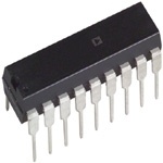
| 描述 | IC MULTIPLEXER 8X1 18DIP多路器开关 IC 8:1 280 Ohm Latchable |
| 产品分类 | |
| 品牌 | Analog Devices |
| 产品手册 | |
| 产品图片 |
|
| rohs | 符合RoHS无铅 / 符合限制有害物质指令(RoHS)规范要求 |
| 产品系列 | 开关 IC,多路器开关 IC,Analog Devices ADG528AKNZ- |
| 数据手册 | |
| 产品型号 | ADG528AKNZ |
| 产品培训模块 | http://www.digikey.cn/PTM/IndividualPTM.page?site=cn&lang=zhs&ptm=16843http://www.digikey.cn/PTM/IndividualPTM.page?site=cn&lang=zhs&ptm=16845 |
| 产品目录页面 | |
| 产品种类 | 多路器开关 IC |
| 传播延迟时间 | 300 ns |
| 供应商器件封装 | 18-PDIP |
| 关闭隔离—典型值 | 68 dB |
| 功能 | 多路复用器 |
| 包装 | 管件 |
| 商标 | Analog Devices |
| 安装类型 | 通孔 |
| 安装风格 | Through Hole |
| 导通电阻 | 700 欧姆 |
| 导通电阻—最大值 | 700 Ohms |
| 封装 | Tube |
| 封装/外壳 | 18-DIP(0.300",7.62mm) |
| 封装/箱体 | PDIP-18 |
| 工作温度 | -40°C ~ 85°C |
| 工作电源电压 | 10.8 V to 16.5 V |
| 工作电源电流 | 600 uA |
| 工厂包装数量 | 20 |
| 开关数量 | 1 |
| 最大功率耗散 | 470 mW |
| 最大工作温度 | + 85 C |
| 最小工作温度 | - 40 C |
| 标准包装 | 20 |
| 特色产品 | http://www.digikey.cn/product-highlights/cn/zh/analog-devices-adg52-54-switches-multiplexers/2995 |
| 电压-电源,单/双 (±) | 10.8 V ~ 16.5 V, ±10.8 V ~ 16.5 V |
| 电压源 | 单/双电源 |
| 电流-电源 | 600µA |
| 电路 | 1 x 8:1 |
| 空闲时间—最大值 | 600 ns |
| 系列 | ADG528A |
| 运行时间—最大值 | 600 ns |
| 通道数量 | 8 Channel |


- 商务部:美国ITC正式对集成电路等产品启动337调查
- 曝三星4nm工艺存在良率问题 高通将骁龙8 Gen1或转产台积电
- 太阳诱电将投资9.5亿元在常州建新厂生产MLCC 预计2023年完工
- 英特尔发布欧洲新工厂建设计划 深化IDM 2.0 战略
- 台积电先进制程称霸业界 有大客户加持明年业绩稳了
- 达到5530亿美元!SIA预计今年全球半导体销售额将创下新高
- 英特尔拟将自动驾驶子公司Mobileye上市 估值或超500亿美元
- 三星加码芯片和SET,合并消费电子和移动部门,撤换高东真等 CEO
- 三星电子宣布重大人事变动 还合并消费电子和移动部门
- 海关总署:前11个月进口集成电路产品价值2.52万亿元 增长14.8%


PDF Datasheet 数据手册内容提取
CMOS Latched 4-/8-Channel Analog Multiplexers ADG528A FEATURES FUNCTIONAL BLOCK DIAGRAMS 44 V Supply Maximum Rating V to V Analog Signal Range SS DD Single-/Dual-Supply Specifications Wide Supply Ranges (10.8 V to 16.5 V) Microprocessor Compatible (100 ns WR Pulse) Extended Plastic Temperature Range (–40°C to +85°C) Low Leakage (20 pA typ) Low Power Dissipation (28 mW max) Available in 18-Lead DIP/SOIC and 20-Lead PLCC Packages Superior Alternative to: DG528 DG529 ADG529A is obsolete GENERAL DESCRIPTION PRODUCT HIGHLIGHTS The ADG528A and ADG529A are CMOS monolithic analog 1. Single-/dual-supply specifications with a wide tolerance. multiplexers with eight channels and four dual channels, respec- The devices are specified in the 10.8 V to 16.5 V range for tively. On-chip latches facilitate microprocessor interfacing. The both single- and dual-supplies. ADG528A switches one of eight inputs to a common output, 2. Easily Interfaced depending on the state of three binary addresses and an enable The ADG528A and ADG529A can be easily interfaced with input. The ADG529A switches one of four differential inputs to microprocessors. The WR signal latches the state of the a common differential output, depending on the state of two address control lines and the enable line. The RS signal binary addresses and an enable input. Both devices have TTL clears both the address and enable data in the latches result- and 5 V CMOS logic-compatible digital inputs. ing in no output (all switches off). RS can be tied to the The ADG528A and ADG529A are designed on an enhanced microprocessor reset pin. LC2MOS process, which gives an increased signal capability of 3. Extended Signal Range VSS to VDD and enables operation over a wide range of supply The enhanced LC2MOS processing results in a high breakdown voltages. The devices can comfortably operate anywhere in the and an increased analog signal range of V to V . 10.8 V to 16.5 V single- or dual-supply range. These SS DD multiplex-ers also feature high switching and low R . 4. Break-Before-Make Switching ON Switches are guaranteed break-before-make so that input signals are protected against momentary shorting. The ADG529A is no longer available. 5. Low Leakage Leakage currents in the range of 20 pA make these multiplexers suitable for high precision circuits.
ADG528A–SPECIFICATIONS DUAL SUPPLY (V = +10.8 V to +16.5 V, V = –10.8 V to –16.5 V, unless otherwise noted.) DD SS ADG528A ADG528A ADG528A ADG529A ADG529A ADG529A K Version B Version T Version –40°C to –40°C to –55°C to Parameter +25°C +85°C +25°C +85°C +25°C +125°C Units Comments ANALOG SWITCH Analog Signal Range V V V V V V V min SS SS SS SS SS SS V V V V V V V max DD DD DD DD DD DD R 280 280 280 Ω typ –10 V ≤ V ≤ +10 V, I = 1 mA; ON S DS Test Circuit 1 450 600 450 600 450 600 Ω max 300 400 300 400 Ω max V = 15 V (±10%), V = –15 V (±10%) DD SS 300 400 Ω max V = 15 V (±5%), V = –15 V (±5%) DD SS R Drift 0.6 0.6 0.6 %/°C typ –10 V ≤ V ≤ +10 V, I = 1 mA ON S DS R Match 5 5 5 % typ –10 V ≤ V ≤ +10 V, I = 1 mA ON S DS I (OFF), Off Input S Leakage 0.02 0.02 0.02 nA typ V1 = ±10 V, V2 = (cid:1)10 V; Test Circuit 2 1 50 1 50 1 50 nA max I (OFF), Off Input D Leakage 0.04 0.04 0.04 nA typ V1 = ±10 V, V2 = (cid:1)10 V; Test Circuit 3 ADG528A 1 100 1 100 1 100 nA max ADG529A 1 50 1 50 1 50 nA max I (ON), On Channel D Leakage 0.04 0.04 0.04 nA typ V1 = ±10 V, V2 = (cid:1)10 V; Test Circuit 4 ADG528A 1 100 1 100 1 100 nA max ADG529A 1 50 1 50 1 50 nA max I , Differential Off DIFF Output Leakage (ADG529A only) 25 25 25 nA max V1 = ±10 V, V2 = (cid:1)10 V; Test Circuit 5 DIGITAL CONTROL V , Input High Voltage 2.4 2.4 2.4 V min INH V , Input Low Voltage 0.8 0.8 0.8 V max INL I or I 1 1 1 µA max V = 0 to V INL INH IN DD C Digital Input IN Capacitance 8 8 8 pF max DYNAMIC CHARACTERISTICS1 t 200 200 200 ns typ V1 = ±10 V, V2 = (cid:1)10 V; Test Circuit 6 TRANSITION 300 400 300 400 300 400 ns max t 50 50 50 ns typ Test Circuit 7 OPEN 25 10 25 10 25 10 ns min t (EN, WR) 200 200 200 ns typ Test Circuits 8 and 9 ON 300 400 300 400 300 400 ns max t (EN, RS) 200 200 200 ns typ Test Circuits 8 and 10 OFF 300 400 300 400 300 400 ns max t Write Pulse Width 100 120 100 120 100 130 ns min See Figure 1 W t Address, S Enable Setup Time 100 100 100 ns min See Figure 1 t , Address, H Enable Hold Time 10 10 10 ns min See Figure 1 t Reset Pulse Width 100 100 100 ns min See Figure 2 RS OFF Isolation 68 68 68 dB typ V = 0.8 V, R = 1 kΩ, C = 15 pF, EN L L 50 50 50 dB min V = 7 V rms, f = 100 kHz S C (OFF) 5 5 5 pF typ V = 0.8 V S EN C (OFF) D ADG528A 22 22 22 pF typ V = 0.8 V EN ADG529A 11 11 11 pF typ Q , Charge Injection 4 4 4 pC typ R = 0 Ω, V = 0 V; Test Circuit 11 INJ S S –2– REV. C
ADG528A ADG528A ADG528A ADG528A ADG529A ADG529A ADG529A K Version B Version T Version –40°C to –40°C to –55°C to Parameter +25°C +85°C +25°C +85°C +25°C +125°C Units Comments POWER SUPPLY I 0.6 0.6 0.6 mA typ V = V or V DD IN INL INH 1.5 1.5 1.5 mA max I 20 20 20 µA typ V = V or V SS IN INL INH 0.2 0.2 0.2 mA max Power Dissipation 10 10 10 mW typ 2.8 2.8 2.8 mW max NOTE 1Sample tested at +25°C to ensure compliance. Specifications subject to change without notice. SINGLE SUPPLY (V = +10.8 V to +16.5 V, V = GND = 0 V, unless otherwise noted.) DD SS ADG528A ADG528A ADG528A ADG529A ADG529A ADG529A K Version B Version T Version –40°C to –40°C to –55°C to Parameter +25°C +85°C +25°C +85°C +25°C +125°C Units Comments ANALOG SWITCH Analog Signal Range GND GND GND GND GND GND V min V V V V V V V max DD DD DD DD DD DD R ON 500 500 500 Ω typ GND ≤ V ≤ +10 V, I = 0.5 mA; S DS Test Circuit 1 700 1000 700 1000 700 1000 Ω max R Drift 0.6 0.6 0.6 %/°C typ GND ≤ V ≤ +10 V, I = 0.5 mA ON S DS R Match 5 5 5 % typ GND ≤ V ≤ +10 V, I = 0.5 mA ON S DS I (OFF), Off Input S Leakage 0.02 0.02 0.02 nA typ V1 = +10 V/GND, V2 = GND/+10 V; 1 50 1 50 1 50 nA max Test Circuit 2 I (OFF), Off Input D Leakage 0.04 0.04 0.04 nA typ V1 = +10 V/GND, V2 = GND/+10 V; ADG528A 1 100 1 100 1 100 nA max Test Circuit 3 ADG529A 1 50 1 50 1 50 nA max I (ON), On Channel D Leakage 0.04 0.04 0.04 nA typ V1 = +10 V/GND, V2 = GND/+10 V; ADG528A 1 100 1 100 1 100 nA max Test Circuit 4 ADG529A 1 50 1 50 1 50 nA max I , Differential Off DIFF Output Leakage (ADG529A only) 25 25 25 nA max V1 = +10 V/GND, V2 = GND/+10 V; Test Circuit 5 DIGITAL CONTROL V , Input High Voltage 2.4 2.4 2.4 V min INH V , Input Low Voltage 0.8 0.8 0.8 V max INL I or I 1 1 1 µA max V = 0 to V INL INH IN DD C Digital Input IN Capacitance 8 8 8 pF max DYNAMIC CHARACTERISTICS1 t 300 300 300 ns typ V1 = +10 V/GND, V2 = GND/+10 V; TRANSITION Test Circuit 6 450 600 450 600 450 600 ns max t 50 50 50 ns typ Test Circuit 7 OPEN 25 10 25 10 25 10 ns min t (EN, WR) 250 250 250 ns typ Test Circuits 8 and 9 ON 450 600 450 600 450 600 ns max t (EN, RS) 250 250 250 ns typ Test Circuits 8 and 10 OFF 450 600 450 600 450 600 ns max t Write Pulse Width 100 120 100 120 100 130 ns min See Figure 1 W REV. C –3–
ADG528A ADG528A ADG528A ADG528A ADG529A ADG529A ADG529A K Version B Version T Version –40°C to –40°C to –55°C to Parameter +25°C +85°C +25°C +85°C +25°C +125°C Units Comments DYNAMIC CHARACTERISTICS1 (Cont’d) t Address, S Enable Setup Time 100 100 100 ns min See Figure 1 t Address, H Enable Hold Time 10 10 10 ns min See Figure 1 t Reset Pulse Width 100 100 100 ns min See Figure 2 RS OFF Isolation 68 68 68 dB typ V = 0.8 V, R = 1 kΩ, C = 15 pF, EN L L 50 50 50 dB min V = 3.5 V rms, f = 100 kHz S C (OFF) 5 5 5 pF typ V = 0.8 V S EN C (OFF) D ADG528A 22 22 22 pF typ V = 0.8 V EN ADG529A 11 11 11 pF typ Q , Charge Injection 4 4 4 pC typ R = 0 Ω, V = 0 V; Test Circuit 11 INJ S S POWER SUPPLY I 0.6 0.6 0.6 mA typ V = V or V DD IN INL INH 1.5 1.5 1.5 mA max Power Dissipation 11 10 10 mW typ 25 25 25 mW max NOTE 1Sample tested at +25°C to ensure compliance. Specifications subject to change without notice. –4– REV. C
ADG528A PIN CONFIGURATIONS ABSOLUTE MAXIMUM RATINGS1 (T = +25°C, unless otherwise noted) A DIP/SOIC PLCC V to V . . . . . . . . . . . . . . . . . . . . . . . . . . . . . . . . . . . . .44 V DD SS V to GND . . . . . . . . . . . . . . . . . . . . . . . . . . . . . . . . . . .25 V DD V to GND . . . . . . . . . . . . . . . . . . . . . . . . . . . . . . . . . . .–25 V SS Analog Inputs2 Voltage at S, D . . . . . . . . .V – 2 V to V + 2 V or 20 mA, SS DD whichever Occurs First Continuous Current, S or D . . . . . . . . . . . . . . . . . . . 20 mA Pulsed Current, S or D 1 ms duration, 10% Duty Cycle . . . . . . . . . . . . . . . 40 mA Digital Inputs1 Voltage at A, EN, WR, RS . . . . . . V – 4 V to V + 4 V or SS DD 20 mA, whichever Occurs First Power Dissipation (Any Package) Up to +75°C .. . . . . . . . . . . . . . . . . . . . . . . . . . . . .470 mW Derates above +75°C . . . . . . . . . . . . . . . . . . . . . . . 6 mW/°C Operating Temperature Commercial (K Version) . . . . . . . . . . . . . . .–40°C to +85°C Industrial (B Version) . . . . . . . . . . . . . . . . .–40°C to +85°C Extended (T Version) . . . . . . . . . . . . . . . .–55°C to +125°C Storage Temperature Range . . . . . . . . . . . . .–65°C to +150°C Lead Temperature (Soldering, 10 sec) . . . . . . . . . . . . +300°C NOTES 1Stresses above those listed under “Absolute Maximum Ratings” may cause permanent damage to the device. This is a stress rating only and functional operation of the device at these or any other conditions above those indicated in the operational sections of this specification is not implied. Exposure to absolute maximum rating conditions for extended periods may affect device reliability. 2Overvoltage at A, EN, WR, RS, S or D will be clamped by diodes. Current should be limited to the maximum rating above. REV. C –5–
ADG528A TRUTH TABLES TIMING DIAGRAMS A2 A1 A0 EN WR RS ON SWITCH PAIR X X X X 1 Retains Previous Switch Condition X X X X X 0 NONE (Address and Enable Latches Cleared) X X X 0 0 1 NONE 0 0 0 1 0 1 1 0 0 1 1 0 1 2 0 1 0 1 0 1 3 0 1 1 1 0 1 4 Figure 1. 1 0 0 1 0 1 5 1 0 1 1 0 1 6 1 1 0 1 0 1 7 1 1 1 1 0 1 8 X = Don’t Care ADG528A A1 A0 EN WR RS ON SWITCH PAIR X X X 1 Retains Previous Switch Condition Figure 2. X X X X 0 NONE (Address and Enable Latches Cleared) Figure 1 shows the timing sequence for latching the switch X X 0 0 1 NONE address and enable inputs. The latches are level sensitive; there- 0 0 1 0 1 1 fore, while WR is held low, the latches are transparent and the 0 1 1 0 1 2 switches respond to the address and enable inputs. This input 1 0 1 0 1 3 data is latched on the rising edge of WR. 1 1 1 0 1 4 Figure 2 shows the Reset Pulse Width, t , and Reset Turn-off RS Time, t (RS). X = Don’t Care ADG529A OFF Note: All digital input signals rise and fall times measured from 10% to 90% of 3 V. t = t = 20 ns. R F –6– REV. C
Typical Performance Characteristics–ADG528A The multiplexers are guaranteed functional with reduced single or dual supplies down to 4.5 V. TPC 1. R as a Function of V(V): Dual Supply TPC 4. Trigger Levels vs. Power Supply Voltage, ON D S Voltage, T = +25°C Dual or Single Supply, T = +25°C A A TPC 2. Leakage Current as a Function of Temperature TPC 5. t vs. Supply Voltage: Dual and TRANSITION (Note: Leakage Currents Reduce as the Supply Single Supplies, T = +25°C A Voltages Reduce) (Note: For V and |V | < 10 V; V1 = V /V , V2 = DD SS DD SS V /V . See Test Circuit 6) SS DD TPC 3. R as a Function of V(V): Single Supply TPC 6. I vs. Supply Voltage: Dual or Single ON D S DD Voltage, T = +25°C Supply, T = +25°C A A REV. C –7–
ADG528A Test Circuits Test Circuit 1. R Test Circuit 4. I (ON) ON D Test Circuit 2. I (OFF) Test Circuit 5. I S DIFF Test Circuit 6. Switching Time of Multiplexer, t Test Circuit 3. I (OFF) TRANSITION D Test Circuit 7. Break-Before-Make Delay, t OPEN –8– REV. C
ADG528A Test Circuit 8. Enable Delay, t (EN), t (EN) ON OFF Test Circuit 9. Write Turn-On Time, t (WR) ON Test Circuit 10. Reset Turn-Off Time, t (RS) OFF Test Circuit 11. Charge Injection REV. C –9–
ADG528A TERMINOLOGY R Ohmic resistance between terminals D and S t (EN) Delay time between the 50% and 10% points of ON OFF R Match Difference between the RON of any two channels the digital input and switch “OFF” condition ON R Drift Change in RON versus temperature t Delay time between the 50% and 90% points of ON TRANSITION I (OFF) Source terminal leakage current when the switch the digital inputs and switch “ON” condition S is off. when switching from one address state to another. I (OFF) Drain terminal leakage current when the switch is t “OFF” time measured between 50% points of D OPEN off. both switches when switching from one address I (ON) Leakage current that flows from the closed switch state to another D into the body. V Maximum input voltage for Logic “0” INL V (V ) Analog voltage on terminal S or D V Minimum input voltage for Logic “1” S D INH C (OFF) Channel input capacitance for “OFF” condition I (I ) Input current of the digital input S INL INH C (OFF) Channel output capacitance for “OFF” condition V Most positive voltage supply D DD C Digital input capacitance V Most negative voltage supply IN SS t (EN) Delay time between the 50% and 90% points of I Positive supply current ON DD the digital input and switch “ON” condition. I Negative supply current SS –10– REV. C
Data Sheet ADG528A OUTLINE DIMENSIONS 0.920 (23.37) 0.900 (22.86) 0.880 (22.35) 18 10 0.280 (7.11) 0.250 (6.35) 1 9 0.240 (6.10) 0.325 (8.26) 0.310 (7.87) 0.100 (2.54) 0.300 (7.62) BSC 0.060 (1.52) 0.195 (4.95) 0.210 (5.33) MAX 0.130 (3.30) MAX 0.115 (2.92) 0.015 0.150 (3.81) (0.38) 0.015 (0.38) 0.130 (3.30) MIN GAUGE 0.115 (2.92) SEATING PLANE 0.014 (0.36) PLANE 0.010 (0.25) 0.022 (0.56) 0.008 (0.20) 0.005 (0.13) 0.430 (10.92) 0.018 (0.46) MIN MAX 0.014 (0.36) 0.070 (1.78) 0.060 (1.52) 0.045 (1.14) COMPLIANTTO JEDEC STANDARDS MS-001 CONTROLLING DIMENSIONSARE IN INCHES; MILLIMETER DIMENSIONS (RCINEOFRPEANRREERENN LCTEEHA EODSNSEL MSY)AAAYNR BDEE AR CROOEU NNNFODIGETUDAR-POEPFDRFOA INSPC RWHIAH ETOEQL UFEIO VORAR LU EHSNAETL ISFN FLDOEEARSDIGS.N. 070706-A Figure 1. 18-Lead Plastic Dual In-Line Package [PDIP] Narrow Body (N-18) Dimensions Shown in inches and (millimeters) 0.180 (4.57) 0.048 (1.22 ) 0.165 (4.19) 0.042 (1.07) 0.056 (1.42) 0.042 (1.07) 0M.I2N0 (0.51) 0.020R (0.50) 3 19 0.021 (0.53) 00..004482 ((11..2027)) 4 IDEPNITNI F1IER 18 (01.0.2570) 0.013 (0.33)0.330 (8.38) BOTTOM TOP VIEW BSC 0.032 (0.81)0.290 (7.37) VIEW (PINS DOWN) 0.026 (0.66) (PINS UP) 8 14 9 13 0.020 0.045 (1.14) (0.R51) 00..335560 ((98..0849))SQ 0.025 (0.64) R 0.120 (3.04) 0.395 (10.03)SQ 0.090 (2.29) 0.385 (9.78) COMPLIANT TO JEDEC STANDARDS MO-047-AA CONTROLLING DIMENSIONS ARE IN INCHES; MILLIMETER DIMENSIONS (IN PARENTHESES) ARE ROUNDED-OFF INCH EQUIVALENTS FOR REFERENCE ONLY AND ARE NOT APPROPRIATE FOR USE IN DESIGN. Figure 2. 20-Lead Plastic Leaded Chip Carrier [PLCC] (P-20) Dimensions shown in inches and (millimeters) Rev. C | Page 11 of 13
ADG528A Data Sheet 0.005 0.098 (2.49) (0.13) MAX 0.310 (7.87) MIN 0.220 (5.59) 18 10 1 9 PIN 1 0.060 (1.52) 0.015 (0.38) 0.320 (8.13) 0.200 (5.08) 0.960 (24.38) MAX MAX 0.290 (7.37) 0.150 (3.81) MIN 0.015 (0.38) 0.200 (5.08) 15° 0.008 (0.20) 0.125 (3.18) 0.100 0.070 (1.78) SEATING 0° 0.023 (0.58) (2.54) 0.030 (0.76) PLANE BSC 0.014 (0.36) CONTROLLING DIMENSIONS ARE IN INCHES; MILLIMETERS DIMENSIONS (IN PARENTHESES) ARE ROUNDED-OFF INCH EQUIVALENTS FOR REFERENCE ONLY AND ARE NOT APPROPRIATE FOR USE IN DESIGN. Figure 3. 18-Lead Ceramic Dual In-Line Package [CERDIP] (Q-18) Dimensions shown in inches and (millimeters) ORDERING GUIDE Model1 Temperature Range Package Description Package Option ADG528AKN −40°C to +85°C 18-Lead Plastic Dual In-Line Package [PDIP] N–18 ADG528AKNZ −40°C to +85°C 18-Lead Plastic Dual In-Line Package [PDIP] N–18 ADG528AKP −40°C to +85°C 20-Lead Plastic Leaded Chip Carrier [PLCC] P–20 ADG528AKP-REEL −40°C to +85°C 20-Lead Plastic Leaded Chip Carrier [PLCC] P–20 ADG528AKPZ −40°C to +85°C 20-Lead Plastic Leaded Chip Carrier [PLCC] P-20 ADG528AKPZ-REEL −40°C to +85°C 20-Lead Plastic Leaded Chip Carrier [PLCC] P-20 ADG528ATQ −55°C to +125°C 18-Lead Ceramic Dual In-Line Package [CERDIP] Q-18 ADG528ABCHIPS −55°C to +125°C DIE 1 Z = RoHS Compliant Part. Rev. C | Page 12 of 13
Data Sheet ADG528A REVISION HISTORY 8/2017—Rev. B to Rev. C Added ADG529A Obsolete Note .................................................... 1 Updated Outline Dimensions ........................................................ 11 Changes to Ordering Guide` ......................................................... 12 10/2004—Rev. A to Rev. B Deleted 20-Lead LCC Package ......................................... Universal Changes to Features .......................................................................... 5 Changes to Ordering Guide ............................................................. 6 SOIC added to DIP Pin Configuration .......................................... 5 ©2004–2017 Analog Devices, Inc. All rights reserved. Trademarks and registered trademarks are the property of their respective owners. D03337-0-8/17(C)