ICGOO在线商城 > 电路保护 > TVS - 混合技术 > ADG467BRSZ
 Datasheet下载
- 型号: ADG467BRSZ
- 制造商: Analog
- 库位|库存: xxxx|xxxx
- 要求:
| 数量阶梯 | 香港交货 | 国内含税 |
| +xxxx | $xxxx | ¥xxxx |
查看当月历史价格
查看今年历史价格
ADG467BRSZ产品简介:
ICGOO电子元器件商城为您提供ADG467BRSZ由Analog设计生产,在icgoo商城现货销售,并且可以通过原厂、代理商等渠道进行代购。 ADG467BRSZ价格参考。AnalogADG467BRSZ封装/规格:TVS - 混合技术, 。您可以下载ADG467BRSZ参考资料、Datasheet数据手册功能说明书,资料中有ADG467BRSZ 详细功能的应用电路图电压和使用方法及教程。
ADG467BRSZ 是由 Analog Devices Inc. 生产的一款 TVS(瞬态电压抑制器)混合技术产品。其主要应用场景包括保护电子电路免受静电放电(ESD)、电气快速瞬变(EFT)和其他瞬态电压事件的损害。以下是该型号的具体应用场景:

1. 通信接口保护:
   ADG467BRSZ 可用于保护各种通信接口,如 USB、HDMI、以太网和 RS-232 等。这些接口容易受到外部设备插入或环境因素引起的瞬态电压影响,使用 TVS 器件可以有效降低损坏风险。

2. 工业自动化设备:
   在工业环境中,由于电磁干扰(EMI)和复杂的电气系统,设备可能面临较高的瞬态电压威胁。ADG467BRSZ 可用于保护控制器、传感器接口和数据总线等关键部件。

3. 汽车电子系统:
   汽车电子系统需要承受极端环境条件,例如点火开关噪声、负载突降和电池反接等。ADG467BRSZ 的高可靠性使其适合应用于车载信息娱乐系统、导航模块和 CAN 总线保护。

4. 消费类电子产品:
   在智能手机、平板电脑和其他便携式设备中,TVS 器件可防止因用户操作(如插拔充电器或耳机)引发的静电放电问题。ADG467BRSZ 提供低电容特性,适合高速信号线路。

5. 电源管理电路:
   对于 DC-DC 转换器、稳压器和其他电源管理模块,ADG467BRSZ 能够抑制输入端可能出现的电压尖峰,确保电路稳定运行。

6. 医疗设备保护:
   医疗设备对可靠性和安全性要求极高,ADG467BRSZ 可用于保护患者监护仪、超声波设备和心电图机等敏感仪器的输入/输出端口。

总之,ADG467BRSZ 凭借其优异的瞬态抑制性能、低泄漏电流和紧凑封装设计,广泛适用于需要高精度和高可靠性的应用场合。在选择具体应用场景时,应根据实际需求评估其工作电压范围、箝位电压和响应时间等参数。
| 参数 | 数值 |
| 产品目录 | |
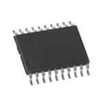
| 描述 | IC CHAN PROTECTOR OCTAL 20-SSOP模拟开关 IC Octal CH Protector |
| 产品分类 | |
| 品牌 | Analog Devices Inc |
| 产品手册 | |
| 产品图片 |
|
| rohs | 符合RoHS无铅 / 符合限制有害物质指令(RoHS)规范要求 |
| 产品系列 | 开关 IC,模拟开关 IC,Analog Devices ADG467BRSZ- |
| 数据手册 | |
| 产品型号 | ADG467BRSZ |
| 产品目录页面 | |
| 产品种类 | 模拟开关 IC |
| 供应商器件封装 | 20-SSOP |
| 功率(W) | - |
| 包装 | 管件 |
| 商标 | Analog Devices |
| 安装风格 | SMD/SMT |
| 封装 | Tube |
| 封装/外壳 | 20-SSOP(0.209",5.30mm 宽) |
| 封装/箱体 | SSOP-20 |
| 工作电源电压 | 20 V |
| 工厂包装数量 | 66 |
| 应用 | 通用 |
| 开关数量 | 8 |
| 开关电压—最大值 | 20 V |
| 技术 | 混合技术 |
| 最大功率耗散 | 15 uW |
| 最大工作温度 | + 85 C |
| 最小工作温度 | - 40 C |
| 标准包装 | 66 |
| 电压-工作 | - |
| 电压-箝位 | ±40V |
| 电源电压-最大 | 20 V |
| 电源电压-最小 | 20 V |
| 电源电流—最大值 | 500 nA |
| 电路数 | 8 |
| 系列 | ADG467 |


- 商务部:美国ITC正式对集成电路等产品启动337调查
- 曝三星4nm工艺存在良率问题 高通将骁龙8 Gen1或转产台积电
- 太阳诱电将投资9.5亿元在常州建新厂生产MLCC 预计2023年完工
- 英特尔发布欧洲新工厂建设计划 深化IDM 2.0 战略
- 台积电先进制程称霸业界 有大客户加持明年业绩稳了
- 达到5530亿美元!SIA预计今年全球半导体销售额将创下新高
- 英特尔拟将自动驾驶子公司Mobileye上市 估值或超500亿美元
- 三星加码芯片和SET,合并消费电子和移动部门,撤换高东真等 CEO
- 三星电子宣布重大人事变动 还合并消费电子和移动部门
- 海关总署:前11个月进口集成电路产品价值2.52万亿元 增长14.8%


PDF Datasheet 数据手册内容提取
Octal Channel Protectors ADG467 FEATURES FUNCTIONAL BLOCK DIAGRAM Fault and overvoltage protection up to ±40 V VDD VSS Signal paths open circuit with power off VD1 VS1 Signal path resistance of R with power on ON 44 V supply maximum ratings VD2 VS2 Low on resistance: 62 Ω typical ±1 nA maximum path current leakage @ +25°C VD3 VS3 Low R match (5 Ω maximum) ON Low power dissipation 0.8 μW typical Latch-up proof construction VIN VD8 VS8 VOUT ADG467 APPLICATIONS VIN VOUT ATE equipment Sensitive measurement equipment VDD VDD Hot insertion rack systems OUTPAUTT VCDLDA M– P1.E5DV 08191-001 Figure 1. GENERAL DESCRIPTION The ADG467 is an octal channel protector. The channel connected and open circuit when power is disconnected. With protector is placed in series with the signal path. The channel power supplies of ±15 V, the on resistance of the ADG467 is protector protects sensitive components from voltage transience 62 Ω typical with a leakage current of ±1 nA maximum. When in the signal path regardless if the power supplies are present or power is disconnected, the input leakage current is approx- not. For this reason, the channel protectors are ideal for use in imately ±0.5 nA typical. applications where correct power sequencing cannot always be The ADG467 is available in an 18-lead SOIC package and a guaranteed (for example, hot insertion rack systems) to protect 20-lead SSOP package. analog inputs. This is described further, and some example PRODUCT HIGHLIGHTS circuits are given in the Applications Information section. 1. Fault Protection. Each channel protector has an independent operation and con- The ADG467 can withstand continuous voltage inputs sists of an N-channel MOSFET, a P-channel MOSFET, and an from −40 V to +40 V. When a fault occurs due to the N-channel MOSFET, connected in series. The channel protector power supplies being turned off or due to an overvoltage behaves just like a series resistor during normal operation, that being applied to the ADG467, the output is clamped. is, (V + 1.5 V) < V < (V − 1.5 V). When a channel’s analog SS IN DD When power is turned off, current is limited to the input exceeds the power supplies (including V and V = 0 V), DD SS microampere level. one of the MOSFETs switches off, clamping the output to either 2. Low Power Dissipation. V + 1.5 V or V − 1.5 V. Circuitry and signal source protec- SS DD 3. Low R . 62 Ω typical. tion is provided in the event of an overvoltage or power loss. ON 4. Trench Isolation Latch-Up Proof Construction. The channel protectors can withstand overvoltage inputs from A dielectric trench separates the p- and n-channel −40 V to +40 V. See the Circuit Information section. MOSFETs thereby preventing latch-up. The ADG467 can operate off both bipolar and unipolar supplies. The channels are normally on when power is Rev. B Information furnished by Analog Devices is believed to be accurate and reliable. However, no responsibility is assumed by Analog Devices for its use, nor for any infringements of patents or other One Technology Way, P.O. Box 9106, Norwood, MA 02062-9106, U.S.A. rights of third parties that may result from its use. Specifications subject to change without notice. No license is granted by implication or otherwise under any patent or patent rights of Analog Devices. Tel: 781.329.4700 www.analog.com Trademarks and registered trademarks are the property of their respective owners. Fax: 781.461.3113 ©2011 Analog Devices, Inc. All rights reserved.
ADG467 TABLE OF CONTENTS Features..............................................................................................1 Typical Performance Characteristics..............................................6 Applications.......................................................................................1 Test Circuits........................................................................................8 Functional Block Diagram..............................................................1 Circuit Information...........................................................................9 General Description.........................................................................1 Overvoltage Protection.................................................................9 Product Highlights...........................................................................1 Trench Isolation..............................................................................11 Revision History...............................................................................2 Applications Information..............................................................12 Specifications.....................................................................................3 Overvoltage and Power Supply Sequencing Protection........12 Dual Supply...................................................................................3 High Voltage Surge Suppression..............................................13 Absolute Maximum Ratings............................................................4 Outline Dimensions.......................................................................14 ESD Caution..................................................................................4 Ordering Guide..........................................................................15 Pin Configuration and Function Descriptions.............................5 REVISION HISTORY 2/11—Rev. A to Rev. B Added Test Circuits Section and Figure 16 to Figure 20..............8 Updated Format..................................................................Universal Changes to Overvoltage Protection Section and Figure 23.........9 Deleted ADG466................................................................Universal Changes to Figure 24......................................................................10 Changes to Features Section, General Description Section, Change to Figure 26.......................................................................11 Figure 1, and Product Highlights Section.....................................1 Changes to Overvoltage and Power Supply Sequencing Changes to Power Requirements, V /V Parameter, Table 1...3 Protection Section and Figure 27.................................................12 DD SS Deleted 8-Lead DIP, SOIC, and μSOIC Pin Configuration........3 Changes to High Voltage Surge Suppression Section and Deleted Figure 12; Renumbered Sequentially..............................5 Figure 28..........................................................................................13 Changes to Figure 4 to Figure 6......................................................6 Changes to Outline Dimensions..................................................14 Added Figure 7; Renumbered Sequentially..................................6 Changes to Ordering Guide..........................................................15 Changes to Figure 11 to Figure 15..................................................7 Rev. B | Page 2 of 16
ADG467 SPECIFICATIONS DUAL SUPPLY V = +15 V, V = −15 V, GND = 0 V, unless otherwise noted. DD SS Table 1. ADG467 Parameter +25°C −40°C to +85°C Unit Test Conditions/Comments FAULT PROTECTED CHANNEL Fault-Free Analog Signal Range V + 1.5 V typ Output open circuit SS V − 1.5 V typ DD V + 1.7 V typ Output loaded, 1 mA SS V − 1.7 V typ DD R 62 80 Ω typ −10 V ≤ V ≤ +10 V, I = 1 mA ON Sx Sx 95 Ω max R Flatness 6 Ω max −5 V ≤ V ≤ +5 V ON Sx R Match between Channels 5 6 Ω max V = ±10 V, I = 1 mA ON Sx Sx LEAKAGE CURRENTS Channel Output Leakage, I V = V = ±10 V S(ON) Sx Dx (Without Fault Condition) ±0.04 ±0.2 nA typ ±1 ±5 nA max Channel Input Leakage, I V = ±25 V D(ON) Sx (with Fault Condition) ±0.2 ±0.4 nA typ V = open circuit Dx ±2 ±5 nA max Channel Input Leakage, I V = 0 V, V = 0 V D(OFF) DD SS (with Power Off and Fault) ±0.5 ±2 nA typ V = ±35 V Sx ±2 ±10 nA max V = open circuit Dx Channel Input Leakage, I V = 0 V, V = 0 V D(OFF) DD SS (with Power Off and Output Short Circuit) ±0.006 ±0.16 μA typ V = ±35 V, V = 0 V Sx Dx ±0.015 ±0.5 μA max POWER REQUIREMENTS I ±0.05 μA typ DD ±0.5 ±8 μA max I ±0.05 μA typ SS ±0.5 ±8 μA max V /V ±4.5/±20 V min/max DD SS Rev. B | Page 3 of 16
ADG467 ABSOLUTE MAXIMUM RATINGS T = +25°C, unless otherwise noted. Stresses above those listed under Absolute Maximum Ratings A may cause permanent damage to the device. This is a stress Table 2. rating only; functional operation of the device at these or any Parameter Rating other conditions above those indicated in the operational VDD to VSS +44 V section of this specification is not implied. Exposure to absolute VSx, VDx, Analog Input Overvoltage with VSS − 20 V to VDD + 20 V maximum rating conditions for extended periods may affect Power On1 device reliability. V , V , Analog Input Overvoltage with −40 V to +40 V Sx Dx Power Off1 Continuous Current, VSx, VDx 20 mA ESD CAUTION Peak Current, V , V (Pulsed at 1 ms, 40 mA Sx Dx 10% Duty Cycle Maximum) Operating Temperature Range Industrial (B Version) −40°C to +85°C Storage Temperature Range −65°C to +125°C Junction Temperature +150°C SOIC Package θ , Thermal Impedance 160°C/W JA Lead Temperature, Soldering Vapor Phase (60 sec) +215°C Infrared (15 sec) +220°C SSOP Package θ , Thermal Impedance 130°C/W JA Lead Temperature, Soldering Vapor Phase (60 sec) +215°C Infrared (15 sec) +220°C 1 Overvoltages at VSx or VDx are clamped by the channel protector; see the Circuit Information section. Rev. B | Page 4 of 16
ADG467 PIN CONFIGURATION AND FUNCTION DESCRIPTIONS VD1 1 20 NC VD1 1 18 VDD VD2 2 19 VDD VD2 2 17 VS1 VD3 3 18 VS1 VVVDDD345 345 (NAToODt PtGo V S4IEc6Wa7le) 111654 VVVSSS234 VVVVDDDD4567 4567 (NAToODt PtGo V S4IEc6Wa7le) 11117654 VVVVSSSS2345 VD6 6 13 VS5 VD8 8 13 VS6 VD7 7 12 VS6 VSS 9 12 VS7 VVSDS8 89 1110 VVSS78 08191-002 NC 10 NC = NO CONNECT11 VS8 08191-003 Figure 2. 18-Lead SOIC Pin Configuration Figure 3. 20-Lead SSOP Pin Configuration Table 3. Pin Function Descriptions Pin No. SOIC SSOP Mnemonic Description 1 1 V Drain Terminal 1. This pin can be an input or an output. D1 2 2 V Drain Terminal 2. This pin can be an input or an output. D2 3 3 V Drain Terminal 3. This pin can be an input or an output. D3 4 4 V Drain Terminal 4. This pin can be an input or an output. D4 5 5 V Drain Terminal 5. This pin can be an input or an output. D5 6 6 V Drain Terminal 6. This pin can be an input or an output. D6 7 7 V Drain Terminal 7. This pin can be an input or an output. D7 8 8 V Drain Terminal 8. This pin can be an input or an output. D8 9 9 V Most Negative Power Supply Potential. In single-supply applications, this pin can be connected to SS ground. N/A 10 NC No Connect. 10 11 V Source Terminal 1. This pin can be an input or an output. S8 11 12 V Source Terminal 2. This pin can be an input or an output. S7 12 13 V Source Terminal 3. This pin can be an input or an output. S6 13 14 V Source Terminal 4. This pin can be an input or an output. S5 14 15 V Source Terminal 5. This pin can be an input or an output. S4 15 16 V Source Terminal 6. This pin can be an input or an output. S3 16 17 V Source Terminal 7. This pin can be an input or an output. S2 17 18 V Source Terminal 8. This pin can be an input or an output. S1 18 19 V Most Positive Power Supply Potential. DD N/A 20 NC No Connect. Do not connect to this pin. Rev. B | Page 5 of 16
ADG467 TYPICAL PERFORMANCE CHARACTERISTICS 100 120 VDD, VSS = ±16.5V 90 VDD, VSS = ±15V 110 80 VVDDDD,, VVSSSS == ±±1230.V5V 100 VVDDDD == 2103V.2V Ω) Ω) VDD = 12V E ( E ( VDD = 10.8V NC 70 NC 90 A A T T S S SI 60 SI 80 E E R R N N O 50 O 70 40 60 TA = 25°C TVAS S= = 2 50°VC 3–019–17–15–13–11–9–7IN–P5U–T3 V–O1LT1AG3E (5V)7 9 111315 171908191-004 501 3 5 7INPUT9 VOLT1A1GE (V1)3 15 17 1908191-007 Figure 4. On Resistance as a Function of VDD and VSx (Input Voltage), Figure 7. On Resistance as a Function of VDD and VSx (Input Voltage), Dual Supply Single Supply 80 VDD = +15V +85°C 75 VSS = –15V +25°C POSITIVE OVERVOLTAGE ON INPUT 70 –+4100°5C°C CRLL == 110000kpΩF CE (Ω) 6650 VVDSSD == –+1100VV –S5TVEPTO IN +P1U5TV N 15V A T 55 S SI 10V E 50 R N CHANNEL PROTECTOR O 45 5V OUTPUT 40 0V 35 –5V 30–10 –8 –6 –4 INP–U2T VO0LTAGE2 (V) 4 6 8 10 08191-005 CH1 5.00V CH2 5.00V M 50.0ns A CH1 500mV 08191-008 Figure 5. On Resistance as a Function of Temperature and VSx (Input Voltage) Figure 8. Positive Overvoltage Transience Response 260 250 224300 VVDDDD,, VVSSSS == ±±55.V5V NEGATIVE OVERVOLTAGE ON INPUT 220 VDD, VSS = ±4.5V 5V CE (Ω)221109000 0V CVRVDSLLS D== = =11 00–+0011kp00ΩVFV N180 –5V CHANNEL PROTECTOR TA170 OUTPUT S SI160 –10V RE150 N 140 O –15V 130 +5VTO –15V 120 STEP INPUT 110 100 90 80–4 –3 –2 IN–P1UT VO0LTAGE 1(V) 2 3 408191-006 CH1 5.00V CH2 5.00V M 50.0ns A CH1 500mV 08191-009 Figure 6. On Resistance as a Function of VDD and VSx (Input Voltage), Figure 9. Negative Overvoltage Transience Response 5 V Dual Supply Rev. B | Page 6 of 16
ADG467 0 VDD = +15V –10VTO +10V INPUT VRDL D= =1 0+05kVΩ –20 TVASS = = 2 5–°1C5V VSS = –5V INPUT = 0dBm 1 20V –40 B) d S ( –60 S VCLAMP = 4.5V LO –80 OUTPUT 2 –100 CH1 5.00V CH2 5.00VVCLAMPM = 140V0µs A CH1 500mV08191-010 –1201k 10k 100kFREQUE1MNCY (Hz)10M 100M 1G08191-013 Figure 10. Overvoltage Ramp Figure 13. Crosstalk Between Adjacent Channels 0 0 –1 VDD = 0V –10 VSS = 0V –2 –20 TA = 25°C –3 INPUT = 0dBm B) –4 –30 OSS (d ––56 dB) –40 RTION L ––78 LOSS ( ––5600 E –9 S IN –10 –70 –11 VDD = +15V –80 –12 VSS = –15V TA = 25°C –90 –13 INPUT = 0dBm –11400k 1M FREQU1E0NMCY (Hz) 100M 1G08191-011 –1001M 10MFREQUENCY (Hz)100M 1G08191-014 Figure 11. Frequency Response (Magnitude) Figure 14. Off Isolation 10 0 –10 11.8ns s) –20 e e gr –30 1 e D SE ( –40 A H P –50 –60 VDD = +15V 12.2ns VSS = –15V –70 TA = 25°C INPUT = 0dBm 2 –81000k 1MFREQUENCY (Hz)10M 100M08191-012 CH1 2.00V CH2 2.00V M 10.0ns A CH1 2.2V08191-015 Figure 12. Frequency Response (Phase) Figure 15. Propagation Delay Rev. B | Page 7 of 16
ADG467 TEST CIRCUITS IDS V1 S D VDD VSS VS RON = V1/IDS 08191-016 0.1µF 0.1µF NETWORK Figure 16. On Resistance VDD VSS ANALYZER S 50Ω IN 50Ω VS D VIN RL VOUT ID(ON) 50Ω S D NC A NC = NO CONNECT VD 08191-017 OFF ISOLATION = 20 logVVOSUT 08191-019 Figure 17. On Leakage Figure 19. Off Isolation VDD VSS VDD VSS 0.1µF 0.1µF 0.1µF 0.1µF NETWORK NETWORK ANALYZER VDD VSS VDD VSS ANALYZER VOUT RL VS1 50Ω S 50Ω VDx RL IN VS VS2 50Ω D VS VIN RL VOUT 50Ω CHANNEL-TO-CHANNEL CROSSTALK = 20 log VVOSUT 08191-018 INSERTION LOSS = 20 logVOVUOTUWTIWTHITOHU STW SIWTCITHCH 08191-020 Figure 18. Channel-to-Channel Crosstalk Figure 20. Bandwidth Rev. B | Page 8 of 16
ADG467 CIRCUIT INFORMATION Figure 21 shows a simplified schematic of a channel protector the output of the channel protector (no load) is clamped at these circuit. The circuit is made up of four MOS transistors—two threshold voltages. However, the channel protector output NMOS and two PMOS. One of the PMOS devices does not lie clamps at a voltage value that is inside these thresholds if the directly in the signal path but is used to connect the source of output is loaded. For example, with an output load of 1 kΩ, V = DD the second PMOS device to its backgate. This has the effect of 15 V, and a positive overvoltage on the input, the output clamps lowering the threshold voltage and thus increasing the input at V − V − ΔV = 15 V − 1.5 V − 0.6 V = 12.9 V, where ΔV is DD TN signal range of the channel for normal operation. The source due to an I × R voltage drop across the channels of the MOS and backgate of the NMOS devices are connected for the same devices (see Figure 23). As can be seen from Figure 23, the current reason. During normal operation, the channel protectors have during fault condition is determined by the load on the output an on resistance of 62 Ω typical. The channel protectors are very (that is, V /R). However, if the supplies are off, the fault CLAMP L low power devices, and even under fault conditions, the supply current is limited to the nano-ampere level. current is limited to sub microampere levels. All transistors are Figure 22, Figure 24, and Figure 25 show the operating condi- dielectrically isolated from each other using a trench isolation tions of the signal path transistors during various fault conditions. method. This makes it impossible to latch up the channel protec- Figure 22 shows how the channel protectors operate when a tors. For further details, see the Trench Isolation section. positive overvoltage is applied to the channel protector. VSS VD(+D1 3–. 5VVTN)1 POSITIVE NMOS PMOS NMOS PMOS OVERVOLTAGE (+20V) NMOS NMOS SATURATED NON- NON- SATURATED SATURATED VDD VSSPMOS VDD 08191-021 1VTN = NMOS THRESHOLVDD DV O(+L1T5AVG)E (+1.5VV)S.S (–15V) VDD (+15V) 08191-022 Figure 21. The Channel Protector Circuit Figure 22. Positive Overvoltage on the Channel Protector OVERVOLTAGE PROTECTION The first NMOS transistor goes into a saturated mode of When a fault condition occurs on the input of a channel protec- operation as the voltage on its drain exceeds the gate voltage tor, the voltage on the input has exceeded some threshold voltage (VDD) − the threshold voltage (VTN). This situation is shown in set by the supply rail voltages. The threshold voltages are related Figure 23. The potential at the source of the NMOS device is to the supply rails as follows. For a positive overvoltage, the equal to VDD − VTN. The other MOS devices are in a nonsatu- threshold voltage is given by V − V , where V is the threshold rated mode of operation. DD TN TN voltage of the NMOS transistor (1.5 V typical). In the case of a negative overvoltage, the threshold voltage is given by V − V , SS TP where V is the threshold voltage of the PMOS device (−1.5 V TP typical). If the input voltage exceeds these threshold voltages, VDx VG VSx V (20V) (VDD = 15V) (13.5V) PMOS NMOS N+ N-CHANNEL N+ P+ NONSATURATED VCLAMP OVERVOLTAGE EFFECTIVE OPERATION RL OPERATION SPACE CHARGE (SATURATED) VT = 1.5VREGIONP– (VO – VTN = 13.5V) IOUT 08191-023 Figure 23. Positive Overvoltages Operation of the Channel Protector Rev. B | Page 9 of 16
ADG467 When a negative overvoltage is applied to the channel protector The channel protector is also functional when the supply rails circuit, the PMOS transistor enters a saturated mode of operation are down (for example, power failure) or momentarily uncon- as the drain voltage exceeds V − V (see Figure 24). As in the nected (for example, rack system). This is where the channel SS TP case of the positive overvoltage, the other MOS devices are protector has an advantage over more conventional protection nonsaturated. methods such as diode clamping (see the Applications Information NEGATIVE section). When VDD and VSS equal 0 V, all transistors are off and OVERVOLTAGE VSS – VTP1 the current is limited to subnano-ampere levels (see Figure 25). (–20V) (–13.5V) (0V) NEGATIVE NMOS PMOS NMOS OVERVOLTAGE (–20V) POSITIVE OR NMOS PMOS NMOS NON- SATURATED NON- NEGATIVE SATURATED SATURATED OVERVOLTAGE OFF OFF OFF 1VTP = PMOS THRESHOLVDD DV O(+L1T5AVG)E (–1.5VV).SS (–15V) VDD (+15V) 08191-024 VDD (0V) VSS (0V) VDD (0V) 08191-025 Figure 24. Negative Overvoltage on the Channel Protector Figure 25. Channel Protector Supplies Equal to 0 V Rev. B | Page 10 of 16
ADG467 TRENCH ISOLATION The MOS devices that make up the channel protector are CMOS devices are normally isolated from each other by isolated from each other by an oxide layer (trench) (see Figure 26). junction isolation. In junction isolation, the N and P wells of the When the NMOS and PMOS devices are not electrically CMOS transistors form a diode that is reverse biased under isolated from each other, parasitic junctions between CMOS normal operation. However, during overvoltage conditions, this transistors may cause latch-up. Latch-up is caused when P-N diode becomes forward biased. A silicon-controlled rectifier junctions that are normally reverse biased become forward (SCR) type circuit is formed by the two transistors causing a biased, causing large currents to flow, which can be destructive. significant amplification of the current that, in turn, leads to latch-up. With trench isolation, this diode is removed; the result is a latch-up-proof circuit. VG VG VSx VDx VSx VDx RT P+ P-CHANNEL P+ RT N+ N-CHANNEL N+ RT E E E N N N CH N– CH P– CH BURIED OXIDE LAYER SUBSTRATE (BACKGATE) 08191-026 Figure 26. Trench Isolation Rev. B | Page 11 of 16
ADG467 APPLICATIONS INFORMATION OVERVOLTAGE AND POWER SUPPLY Figure 27 shows a typical application that requires overvoltage SEQUENCING PROTECTION and power supply sequencing protection. The application shows a hot insertion rack system. This involves plugging a circuit The ADG467 is ideal for use in applications where input overvol- board or module into a live rack via an edge connector. In this tage protection is required and correct power supply sequencing type of application, it is not possible to guarantee correct power cannot always be guaranteed. The overvoltage protection ensures supply sequencing. Correct power supply sequencing means that the output voltage of the channel protector does not exceed the that the power supplies should be connected before any external threshold voltages set by the supplies (see the Circuit Information signals. Incorrect power sequencing can cause a CMOS device section) when there is an overvoltage on the input. When the to latch up. This is true of most CMOS devices regardless of the input voltage does not exceed these threshold voltages, the channel functionality. RC networks are used on the supplies of the channel protector behaves like a series resistor (62 Ω typical). The resis- protector (see Figure 27) to ensure that the rest of the circuitry tance of the channel protector does vary slightly with operating is powered up before the channel protectors. In this way, the conditions (see the Typical Performance Characteristics outputs of the channel protectors are clamped well below V section). DD and V until the capacitors are charged. The diodes ensure that SS The power sequencing protection is provided by the channel the supplies on the channel protector never exceed the supply protector, which becomes a high resistance device when the rails of the board when it is being disconnected. This ensures supplies to the channel protector are not connected. Under this that signals on the inputs of the CMOS devices never exceed the condition, all transistors in the channel protector are off and the supplies. only currents that flow are leakage currents, which are at the microampere level. EDGE CONNECTOR VDD +5V VSS –5V ANALOG IN VD1 VS1 ADC –2.5VTO +2.5V VD2 VS2 LOGIC VD3 VS3 LOGIC VD4 VS4 LOGIC CONTROL LOGIC VD5 VS5 LOGIC VD6 VS6 LOGIC VD7 VS7 LOGIC VD8 VS8 LOGIC ADG467 GND 08191-027 Figure 27. Overvoltage and Power Supply Sequencing Protection Rev. B | Page 12 of 16
ADG467 HIGH VOLTAGE SURGE SUPPRESSION voltage of a TVS is the normal peak operating voltage of the circuit. Also, a TVS offers no protection against latch-up of The ADG467 is not intended for use in high voltage applications sensitive CMOS devices when the power supplies are off. The like surge suppression. The ADG467 has breakdown voltages in ideal solution is to use a channel protector in conjunction with excess of V − 20 V and V + 20 V on the inputs when the SS DD a TVS to provide the optimal leakage current specification and power supplies are connected. When the power supplies are circuit protection. disconnected, the breakdown voltages on the input of the Figure 28 shows an input protection scheme that uses both a channel protector are ±40 V. In applications where inputs are TVS and a channel protector. The TVS is selected with a reverse likely to be subject to overvoltages exceeding the breakdown standoff voltage that is much greater than the operating voltage voltages specified for the channel protectors, transient voltage of the circuit (TVSs with higher breakdown voltages tend to suppressors (TVSs) should be used. These devices are have better standby leakage current specifications) but is inside commonly used to protect vulnerable circuits from electric the breakdown voltage of the channel protector. This circuit overstress such as that caused by electrostatic discharge, protects the circuitry regardless of whether the power supplies inductive load switching, and induced lightning. However, are present. TVSs can have a substantial standby (leakage) current (300 μA typical) at the reverse standoff voltage. The reverse stand-off VDD= +5V VSS= –5V VD1 VS1 VD2 VS2 VD3 VS3 VD4 VS4 ADC VD5 VS5 VD6 VS6 VD7 VS7 VD8 VS8 ADG467 TVVOSLsT ABGREE A= K2D0VOWN 08191-028 Figure 28. High Voltage Protection Rev. B | Page 13 of 16
ADG467 OUTLINE DIMENSIONS 11.75 (0.4626) 11.35 (0.4469) 18 10 7.60 (0.2992) 7.40 (0.2913) 1 10.65 (0.4193) 9 10.00 (0.3937) 0.75 (0.0295) 45° 2.65 (0.1043) 0.25 (0.0098) 0.30 (0.0118) 2.35 (0.0925) 8° 0.10 (0.0039) 0° COPLANARITY 0.10 (0.10.52070) 00..5311 ((00..00210212)) SPLEAATNIENG 00..3230 ((00..00103709)) 10..2470 ((00..00510507)) BSC COMPLIANTTO JEDEC STANDARDS MS-013-AB C(RINOEFNPEATRRREOENNLCLTEIHN EOGSN EDLSIYM)AEANNRDSEI AORRNOESU NANORDEET DAIN-PO MPFRIFLO LMPIIMRLELIATIMTEEER TFSEO; RIRN ECUQHSU EDI VIINMA LEDENENSSTIIOGSN NFS.OR 060706-A Figure 29. 18-Lead Standard Small Outline Package [SOIC_W] Wide Body (RW-18) Dimensions shown in millimeters and (inches) 7.50 7.20 6.90 20 11 5.60 5.30 5.00 8.20 7.80 1 7.40 10 1.85 0.25 2.00 MAX 1.75 0.09 1.65 COPLA0N.0A5R MITIYN 0.65 BSC 00..3282 SPELAATNIENG 840°°° 000...975555 0.10 COMPLIANTTO JEDEC STANDARDS MO-150-AE 060106-A Figure 30. 20-Lead Shrink Small Outline Package [SSOP] (RS-20) Dimensions shown in millimeters Rev. B | Page 14 of 16
ADG467 ORDERING GUIDE Model1 Temperature Range Package Description Package Option ADG467BR −40°C to +85°C 18-Lead Standard Small Outline Package [SOIC_W] RW-18 ADG467BR-REEL −40°C to +85°C 18-Lead Standard Small Outline Package [SOIC_W] RW-18 ADG467BR-REEL7 −40°C to +85°C 18-Lead Standard Small Outline Package [SOIC_W] RW-18 ADG467BRZ −40°C to +85°C 18-Lead Standard Small Outline Package [SOIC_W] RW-18 ADG467BRZ-REEL −40°C to +85°C 18-Lead Standard Small Outline Package [SOIC_W] RW-18 ADG467BRZ-REEL7 −40°C to +85°C 18-Lead Standard Small Outline Package [SOIC_W] RW-18 ADG467BRS −40°C to +85°C 20-Lead Shrink Small Outline Package [SSOP] RS-20 ADG467BRS-REEL −40°C to +85°C 20-Lead Shrink Small Outline Package [SSOP] RS-20 ADG467BRSZ −40°C to +85°C 20-Lead Shrink Small Outline Package [SSOP] RS-20 ADG467BRSZ-REEL −40°C to +85°C 20-Lead Shrink Small Outline Package [SSOP] RS-20 1 Z = RoHS Compliant Part. Rev. B | Page 15 of 16
ADG467 NOTES ©2011 Analog Devices, Inc. All rights reserved. Trademarks and registered trademarks are the property of their respective owners. D08191-0-2/11(B) Rev. B | Page 16 of 16
Mouser Electronics Authorized Distributor Click to View Pricing, Inventory, Delivery & Lifecycle Information: A nalog Devices Inc.: ADG467BRZ-REEL7 ADG467BRSZ ADG467BRZ ADG467BR ADG467BR-REEL7 ADG467BRS ADG467BRSZ- REEL ADG467BRS-REEL ADG467BRZ-REEL ADG467BR-REEL