ICGOO在线商城 > 集成电路(IC) > 数据采集 - 模数转换器 > ADC124S101CIMM/NOPB
- 型号: ADC124S101CIMM/NOPB
- 制造商: Texas Instruments
- 库位|库存: xxxx|xxxx
- 要求:
| 数量阶梯 | 香港交货 | 国内含税 |
| +xxxx | $xxxx | ¥xxxx |
查看当月历史价格
查看今年历史价格
ADC124S101CIMM/NOPB产品简介:
ICGOO电子元器件商城为您提供ADC124S101CIMM/NOPB由Texas Instruments设计生产,在icgoo商城现货销售,并且可以通过原厂、代理商等渠道进行代购。 ADC124S101CIMM/NOPB价格参考¥33.26-¥54.70。Texas InstrumentsADC124S101CIMM/NOPB封装/规格:数据采集 - 模数转换器, 12 Bit Analog to Digital Converter 4 Input 1 SAR 10-VSSOP。您可以下载ADC124S101CIMM/NOPB参考资料、Datasheet数据手册功能说明书,资料中有ADC124S101CIMM/NOPB 详细功能的应用电路图电压和使用方法及教程。
| 参数 | 数值 |
| 产品目录 | 集成电路 (IC)半导体 |
| 描述 | IC ADC 12BIT 4CHAN 1MSPS 10MSOP模数转换器 - ADC 4-CH 500ksps-1Msps 12B A/D Cnvtr |
| 产品分类 | |
| 品牌 | Texas Instruments |
| 产品手册 | |
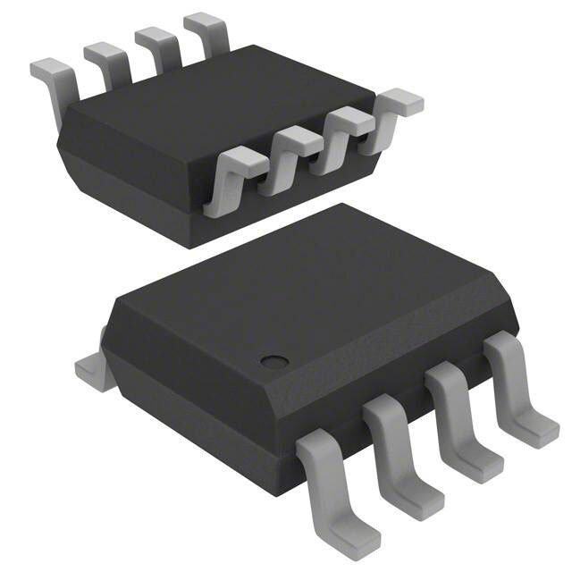
| 产品图片 |
|
| rohs | 符合RoHS无铅 / 符合限制有害物质指令(RoHS)规范要求 |
| 产品系列 | 数据转换器IC,模数转换器 - ADC,Texas Instruments ADC124S101CIMM/NOPB- |
| 数据手册 | |
| 产品型号 | ADC124S101CIMM/NOPB |
| 产品目录页面 | |
| 产品种类 | 模数转换器 - ADC |
| 位数 | 12 |
| 供应商器件封装 | 10-VSSOP |
| 信噪比 | 72.4 dB |
| 其它名称 | *ADC124S101CIMM/NOPB |
| 分辨率 | 12 bit |
| 包装 | 剪切带 (CT) |
| 商标 | Texas Instruments |
| 安装类型 | 表面贴装 |
| 安装风格 | SMD/SMT |
| 封装 | Reel |
| 封装/外壳 | 10-TFSOP,10-MSOP(0.118",3.00mm 宽) |
| 封装/箱体 | MSOP |
| 工作温度 | -40°C ~ 85°C |
| 工作电源电压 | 3.3 V, 5 V |
| 工厂包装数量 | 1000 |
| 接口类型 | Serial (4-Wire, Microwire, QSPI, SPI) |
| 数据接口 | DSP,MICROWIRE™,QSPI™,串行,SPI™ |
| 最大工作温度 | + 85 C |
| 最小工作温度 | - 40 C |
| 标准包装 | 1 |
| 特性 | - |
| 电压参考 | Supply |
| 电压源 | 单电源 |
| 系列 | ADC124S101 |
| 结构 | SAR |
| 转换器数 | 1 |
| 转换器数量 | 1 |
| 转换速率 | 1 MS/s |
| 输入数和类型 | 4 个单端,单极 |
| 输入类型 | Differential |
| 通道数量 | 4 Channel |
| 配用 | /product-detail/zh/ADC124S101EVAL/ADC124S101EVAL-ND/1640518 |
| 采样率(每秒) | 500k ~ 1M |




- 商务部:美国ITC正式对集成电路等产品启动337调查
- 曝三星4nm工艺存在良率问题 高通将骁龙8 Gen1或转产台积电
- 太阳诱电将投资9.5亿元在常州建新厂生产MLCC 预计2023年完工
- 英特尔发布欧洲新工厂建设计划 深化IDM 2.0 战略
- 台积电先进制程称霸业界 有大客户加持明年业绩稳了
- 达到5530亿美元!SIA预计今年全球半导体销售额将创下新高
- 英特尔拟将自动驾驶子公司Mobileye上市 估值或超500亿美元
- 三星加码芯片和SET,合并消费电子和移动部门,撤换高东真等 CEO
- 三星电子宣布重大人事变动 还合并消费电子和移动部门
- 海关总署:前11个月进口集成电路产品价值2.52万亿元 增长14.8%


PDF Datasheet 数据手册内容提取
ADC124S101 www.ti.com SNAS283D–MARCH2005–REVISEDMARCH2013 ADC124S101 4 Channel, 500 ksps to 1 Msps, 12-Bit A/D Converter CheckforSamples:ADC124S101 FEATURES DESCRIPTION 1 • SpecifiedOveraRangeofSampleRates The ADC124S101 is a low-power, four-channel 2 CMOS 12-bit analog-to-digital converter with a high- • FourInputChannels speed serial interface. Unlike the conventional • VariablePowerManagement practice of specifying performance at a single sample • SinglePowerSupplywith2.7V-5.25Vrange rate only, the ADC124S101 is fully specified over a sample rate range of 500 ksps to 1 Msps. The APPLICATIONS converter is based on a successive-approximation register architecture with an internal track-and-hold • PortableSystems circuit. It can be configured to accept up to four input • RemoteDataAcquisition signalsatinputsIN1throughIN4. • InstrumentationandControlSystems The output serial data is straight binary, and is compatible with several standards, such as SPI™, KEY SPECIFICATIONS QSPI™, MICROWIRE, and many common DSP serialinterfaces. • DNL:+0.9/−0.6LSB(typ) The ADC124S101 operates with a single supply that • INL:±0.64LSB(typ) can range from +2.7V to +5.25V. Normal power • SNR:72.4dB(typ) consumption using a +3V or +5V supply is 4.3 mW • PowerConsumption and 13.1 mW, respectively. The power-down feature – 3VSupply:4.3mW(typ) reducesthepowerconsumptiontojust0.14µWusing a+3Vsupply,or0.32µWusinga+5Vsupply. – 5VSupply:13.1mW(typ) The ADC124S101 is available in a 10-lead VSSOP package. Operation over the industrial temperature rangeof−40°Cto+85°C. Thesedeviceshavelimitedbuilt-inESDprotection.Theleadsshouldbeshortedtogetherorthedeviceplacedinconductivefoam duringstorageorhandlingtopreventelectrostaticdamagetotheMOSgates. Table1.PIN-COMPATIBLEALTERNATIVESBYRESOLUTIONANDSPEED(1) Resolution SpecifiedforSampleRateRangeof: 50to200ksps 200to500ksps 500kspsto1Msps 12-bit ADC124S021 ADC124S051 ADC124S101 10-bit ADC104S021 ADC104S051 ADC104S101 8-bit ADC084S021 ADC084S051 ADC084S101 (1) Alldevicesarefullypinandfunctioncompatible. Connection Diagram CS 1 10 SCLK VA 2 9 DOUT ADC124S101 GND 3 8 DIN IN4 4 7 IN1 IN3 5 6 IN2 Figure1. 10-LeadVSSOP SeeDGSPackage 1 Pleasebeawarethatanimportantnoticeconcerningavailability,standardwarranty,anduseincriticalapplicationsof TexasInstrumentssemiconductorproductsanddisclaimerstheretoappearsattheendofthisdatasheet. Alltrademarksarethepropertyoftheirrespectiveowners. 2 PRODUCTIONDATAinformationiscurrentasofpublicationdate. Copyright©2005–2013,TexasInstrumentsIncorporated Products conform to specifications per the terms of the Texas Instruments standard warranty. Production processing does not necessarilyincludetestingofallparameters.
ADC124S101 SNAS283D–MARCH2005–REVISEDMARCH2013 www.ti.com Block Diagram IN1 . 12-Bit VA . MUX T/H SUCCESSIVE APPROXIMATION . ADC GND IN4 GND SCLK CONTROL CS LOGIC DIN DOUT Figure2. PINDESCRIPTIONSANDEQUIVALENTCIRCUITS PinNo. Symbol Description ANALOGI/O 4-7 IN1toIN4 Analoginputs.Thesesignalscanrangefrom0VtoV . A DIGITALI/O 10 SCLK Digitalclockinput.Thisclockdirectlycontrolstheconversionandreadoutprocesses. 9 DOUT Digitaldataoutput.TheoutputsamplesareclockedoutofthispinonfallingedgesoftheSCLKpin. Digitaldatainput.TheADC124S101'sControlRegisterisloadedthroughthispinonrisingedgesof 8 DIN theSCLKpin. Chipselect.OnthefallingedgeofCS,aconversionprocessbegins.Conversionscontinueaslong 1 CS asCSisheldlow. POWERSUPPLY Positivesupplypin.Thispinshouldbeconnectedtoaquiet+2.7Vto+5.25Vsourceandbypassed 2 V toGNDwitha1µFcapacitoranda0.1µFmonolithiccapacitorlocatedwithin1cmofthepower A pin. 3 GND Thegroundreturnforthesupplyandsignals. 2 SubmitDocumentationFeedback Copyright©2005–2013,TexasInstrumentsIncorporated ProductFolderLinks:ADC124S101
ADC124S101 www.ti.com SNAS283D–MARCH2005–REVISEDMARCH2013 Absolute Maximum Ratings(1)(2)(3) SupplyVoltageV −0.3Vto6.5V A VoltageonAnyPintoGND −0.3VtoV +0.3V A InputCurrentatAnyPin (4) ±10mA PackageInputCurrent(4) ±20mA PowerConsumptionatT =25°C See (5) A ESDSusceptibility (6) HumanBodyModel 2500V MachineModel 250V JunctionTemperature +150°C StorageTemperature −65°Cto+150°C (1) AbsoluteMaximumRatingsindicatelimitsbeyondwhichdamagetothedevicemayoccur.OperatingRatingsindicateconditionsfor whichthedeviceisfunctional,butdonotensurespecificperformancelimits.Forensuredspecificationsandtestconditions,seethe ElectricalCharacteristics.Theensuredspecificationsapplyonlyforthetestconditionslisted.Someperformancecharacteristicsmay degradewhenthedeviceisnotoperatedunderthelistedtestconditions. (2) AllvoltagesaremeasuredwithrespecttoGND=0V,unlessotherwisespecified. (3) IfMilitary/Aerospacespecifieddevicesarerequired,pleasecontacttheTISalesOffice/Distributorsforavailabilityandspecifications. (4) Whentheinputvoltageatanypinexceedsthepowersupply(thatis,V <GNDorV >V ),thecurrentatthatpinshouldbelimitedto IN IN A 10mA.The20mAmaximumpackageinputcurrentratinglimitsthenumberofpinsthatcansafelyexceedthepowersupplieswithan inputcurrentof10mAtotwo.TheAbsoluteMaximumRatingspecificationdoesnotapplytotheV pin.ThecurrentintotheV pinis A A limitedbytheAnalogSupplyVoltagespecification. (5) Theabsolutemaximumjunctiontemperature(Tmax)forthisdeviceis150°C.Themaximumallowablepowerdissipationisdictatedby J Tmax,thejunction-to-ambientthermalresistance(θ ),andtheambienttemperature(T ),andcanbecalculatedusingtheformula J JA A P MAX=(Tmax−T )/θ .Thevaluesformaximumpowerdissipationlistedabovewillbereachedonlywhenthedeviceisoperatedin D J A JA aseverefaultcondition(e.g.wheninputoroutputpinsaredrivenbeyondthepowersupplyvoltages,orthepowersupplypolarityis reversed).Obviously,suchconditionsshouldalwaysbeavoided. (6) Humanbodymodelis100pFcapacitordischargedthrougha1.5kΩresistor.Machinemodelis220pFdischargedthroughzeroohms. Operating Ratings(1)(2) OperatingTemperatureRange −40°C≤T ≤+85°C A V SupplyVoltage +2.7Vto+5.25V A DigitalInputPinsVoltageRange −0.3VtoV A ClockFrequency 50kHzto16MHz AnalogInputVoltage 0VtoV A (1) AbsoluteMaximumRatingsindicatelimitsbeyondwhichdamagetothedevicemayoccur.OperatingRatingsindicateconditionsfor whichthedeviceisfunctional,butdonotensurespecificperformancelimits.Forensuredspecificationsandtestconditions,seethe ElectricalCharacteristics.Theensuredspecificationsapplyonlyforthetestconditionslisted.Someperformancecharacteristicsmay degradewhenthedeviceisnotoperatedunderthelistedtestconditions. (2) AllvoltagesaremeasuredwithrespecttoGND=0V,unlessotherwisespecified. Package Thermal Resistance(1)(2) Package θ JA 10-leadVSSOP 190°C/W (1) SolderingprocessmustcomplywithTI'sReflowTemperatureProfilespecifications. (2) Reflowtemperatureprofilesaredifferentforlead-freeandnon-lead-freepackages. Copyright©2005–2013,TexasInstrumentsIncorporated SubmitDocumentationFeedback 3 ProductFolderLinks:ADC124S101
ADC124S101 SNAS283D–MARCH2005–REVISEDMARCH2013 www.ti.com ADC124S101 Converter Electrical Characteristics(1) ThefollowingspecificationsapplyforV =+2.7Vto5.25V,GND=0V,f =8to16MHz,f =500kspsto1Msps, A SCLK SAMPLE C =35pF,unlessotherwisenoted.BoldfacelimitsapplyforT =T toT :allotherlimitsT =25°C. L A MIN MAX A Symbol Parameter Conditions Typical Limits(2) Units STATICCONVERTERCHARACTERISTICS ResolutionwithNoMissingCodes 12 Bits +0.64 +1.6 LSB(max) INL IntegralNon-Linearity −0.64 −1.2 LSB(min) +0.9 +1.6 LSB(max) DNL DifferentialNon-Linearity −0.6 −1.0 LSB(min) V OffsetError 0.44 ±1.3 LSB(max) OFF OEM ChanneltoChannelOffsetErrorMatch ±0.1 ±1.0 LSB(max) FSE FullScaleError −0.34 ±1.5 LSB(max) ChanneltoChannelFull-ScaleError FSEM ±0.1 ±1.0 LSB(max) Match DYNAMICCONVERTERCHARACTERISTICS V =+2.7Vto5.25V SINAD Signal-to-NoisePlusDistortionRatio A 72 69.2 dB(min) f =40.3kHz,−0.02dBFS IN V =+2.7Vto5.25V SNR Signal-to-NoiseRatio A 72.4 70.6 dB(min) f =40.3kHz,−0.02dBFS IN V =+2.7Vto5.25V THD TotalHarmonicDistortion A −82 −75 dB(max) f =40.3kHz,−0.02dBFS IN V =+2.7Vto5.25V SFDR Spurious-FreeDynamicRange A 83 76 dB(min) f =40.3kHz,−0.02dBFS IN ENOB EffectiveNumberofBits V =+2.7Vto5.25V 11.7 11.2 Bits(min) A V =+5.25V Channel-to-ChannelCrosstalk A −86 dB f =40.3kHz IN IntermodulationDistortion,Second V =+5.25V A −87 dB OrderTerms f =40.161kHz,f =41.015kHz a b IMD IntermodulationDistortion,ThirdOrder V =+5.25V A −88 dB Terms f =40.161kHz,f =41.015kHz a b V =+5V 11 MHz A FPBW -3dBFullPowerBandwidth V =+3V 8 MHz A ANALOGINPUTCHARACTERISTICS V InputRange 0toV V IN A I DCLeakageCurrent ±0.02 ±1 µA(max) DCL TrackMode 33 pF C InputCapacitance INA HoldMode 3 pF DIGITALINPUTCHARACTERISTICS V =+5.25V 2.4 V(min) A V InputHighVoltage IH V =+3.6V 2.1 V(min) A V InputLowVoltage 0.8 V(max) IL I InputCurrent V =0VorV ±0.1 ±10 µA(max) IN IN A C DigitalInputCapacitance 2 4 pF(max) IND DIGITALOUTPUTCHARACTERISTICS I =200µA V −0.03 V −0.5 V(min) SOURCE A A V OutputHighVoltage OH I =1mA V −0.10 SOURCE A I =200µA 0.02 0.4 V(max) SINK V OutputLowVoltage OL I =1mA 0.1 SINK I ,I TRI-STATELeakageCurrent ±1 µA(max) OZH OZL (1) Min/maxspecificationlimitsarespecifiedbydesign,test,orstatisticalanalysis. (2) TestedlimitsarespecifiedtoAOQL(AverageOutgoingQualityLevel). 4 SubmitDocumentationFeedback Copyright©2005–2013,TexasInstrumentsIncorporated ProductFolderLinks:ADC124S101
ADC124S101 www.ti.com SNAS283D–MARCH2005–REVISEDMARCH2013 ADC124S101 Converter Electrical Characteristics(1) (continued) ThefollowingspecificationsapplyforV =+2.7Vto5.25V,GND=0V,f =8to16MHz,f =500kspsto1Msps, A SCLK SAMPLE C =35pF,unlessotherwisenoted.BoldfacelimitsapplyforT =T toT :allotherlimitsT =25°C. L A MIN MAX A Symbol Parameter Conditions Typical Limits(2) Units C TRI-STATEOutputCapacitance 2 4 pF(max) OUT OutputCoding Straight(Natural)Binary POWERSUPPLYCHARACTERISTICS(C =10pF) L 2.7 V(min) V SupplyVoltage A 5.25 V(max) V =+5.25V, A 2.5 3.0 mA(max) SupplyCurrent,NormalMode fSAMPLE=1Msps,fIN=40kHz (Operational,CSlow) V =+3.6V, A 1.2 1.6 mA(max) f =1Msps,f =40kHz SAMPLE IN I A V =+5.25V, A 60 nA f =0ksps SAMPLE SupplyCurrent,Shutdown(CShigh) V =+3.6V, A 38 nA f =0ksps SAMPLE PowerConsumption,NormalMode VA=+5.25V 13.1 15.8 mW(max) (Operational,CSlow) V =+3.6V 4.3 5.8 mW(max) A P D PowerConsumption,Shutdown(CS VA=+5.25V 0.32 µW high) V =+3.6V 0.14 µW A ACELECTRICALCHARACTERISTICS 8 MHz(min) f MaximumClockFrequency See(3) SCLK 16 MHz(max) 500 ksps(min) f SampleRate See(3) S 1 Msps(max) t ConversionTime 13 SCLKcycles CONV 30 %(min) DC SCLKDutyCycle f =16MHz 50 SCLK 70 %(max) t Track/HoldAcquisitionTime Full-ScaleStepInput 3 SCLKcycles ACQ ThroughputTime AcquisitionTime+ConversionTime 16 SCLKcycles (3) Thisisthefrequencyrangeoverwhichtheelectricalperformanceisspecified.Thedeviceisfunctionaloverawiderrangewhichis specifiedunderOperatingRatings. ADC124S101 Timing Specifications ThefollowingspecificationsapplyforV =+2.7Vto5.25V,GND=0V,f =8MHzto16MHz,f =500kspsto A SCLK SAMPLE 1Msps,C =35pF,BoldfacelimitsapplyforT =T toT :allotherlimitsT =25°C. L A MIN MAX A Symbol Parameter Conditions Typical Limits(1) Units V =+3.0V −3.5 t SetupTimeSCLKHightoCSFallingEdge See(2) A 10 ns(min) CSU V =+5.0V −0.5 A V =+3.0V +4.5 t HoldtimeSCLKLowtoCSFallingEdge See(2) A 10 ns(min) CLH V =+5.0V +1.5 A V =+3.0V +4 A t DelayfromCSUntilDOUTactive 30 ns(max) EN V =+5.0V +2 A V =+3.0V +14.5 A t DataAccessTimeafterSCLKFallingEdge 30 ns(max) ACC V =+5.0V +13 A t DataSetupTimePriortoSCLKRisingEdge +3 10 ns(min) SU t DataValidSCLKHoldTime +3 10 ns(min) H t SCLKHighPulseWidth 0.5xt 0.3xt ns(min) CH SCLK SCLK (1) TestedlimitsarespecifiedtoAOQL(AverageOutgoingQualityLevel). (2) ClockmaybeeitherhighorlowwhenCSisassertedaslongassetupandholdtimest andt arestrictlyobserved. CSU CLH Copyright©2005–2013,TexasInstrumentsIncorporated SubmitDocumentationFeedback 5 ProductFolderLinks:ADC124S101
ADC124S101 SNAS283D–MARCH2005–REVISEDMARCH2013 www.ti.com ADC124S101 Timing Specifications (continued) ThefollowingspecificationsapplyforV =+2.7Vto5.25V,GND=0V,f =8MHzto16MHz,f =500kspsto A SCLK SAMPLE 1Msps,C =35pF,BoldfacelimitsapplyforT =T toT :allotherlimitsT =25°C. L A MIN MAX A Symbol Parameter Conditions Typical Limits(1) Units t SCLKLowPulseWidth 0.5xt 0.3xt ns(min) CL SCLK SCLK V =+3.0V 1.8 A OutputFalling V =+5.0V 1.3 A t CSRisingEdgetoDOUTHigh-Impedance 20 ns(max) DIS V =+3.0V 1.0 A OutputRising V =+5.0V 1.0 A Timing Diagrams Power Down Power Up Power Up Track Hold Track Hold CS 1 2 3 4 5 6 7 8 9 10 11 12 13 14 15 16 1 2 3 4 5 6 7 8 9 10 SCLK Control register Control register DIN b7 b6 b5 b4 b3 b2 b1 b0 b7 b6 b5 b4 b3 b2 b1 b0 DOUT DB11 DB10 DB9 DB8 DB7 DB6 DB5 DB4 DB3 DB2 DB1 DB0 DB11DB10 DB9 DB8 DB7 Figure3. ADC124S101TimingDiagram IOL 200 PA To Output Pin 1.6V CL 35 pF IOH 200 PA Figure4. TimingTestCircuit 6 SubmitDocumentationFeedback Copyright©2005–2013,TexasInstrumentsIncorporated ProductFolderLinks:ADC124S101
ADC124S101 www.ti.com SNAS283D–MARCH2005–REVISEDMARCH2013 CS tACQ tCONVERT tCH SCLK 1 2 3 4 5 6 7 8 16 tEN tCL tACC tDIS DOUT Z3 Z2 Z1 Z0 DB11 DB10 DB9 DB8 DB1 DB0 tH tSU DIN DONT DONTC ADD2 ADD1 ADD0 DONTC DONTC DONTC Figure5. ADC124S101SerialTimingDiagram CS tCSU SCLK tCLH SCLK Figure6. SCLKandCSTimingParameters Specification Definitions ACQUISITIONTIME isthetimerequiredtoacquiretheinputvoltage.Thatis,itistimerequiredforthehold capacitortochargeuptotheinputvoltage. APERTUREDELAY isthetimebetweenthefourthfallingSCLKedgeofaconversionandthetimewhenthe inputsignalisacquiredorheldforconversion. CONVERSIONTIME isthetimerequired,aftertheinputvoltageisacquired,fortheADCtoconverttheinput voltagetoadigitalword. CROSSTALK isthecouplingofenergyfromonechannelintotheotherchannel,ortheamountofsignalenergy fromoneanaloginputthatappearsatthemeasuredanaloginput. DIFFERENTIALNON-LINEARITY(DNL) isthemeasureofthemaximumdeviationfromtheidealstepsizeof1 LSB. DUTYCYCLE istheratioofthetimethatarepetitivedigitalwaveformishightothetotaltimeofoneperiod.The specificationherereferstotheSCLK. EFFECTIVENUMBEROFBITS(ENOB,orEFFECTIVEBITS) isanothermethodofspecifyingSignal-to-Noise andDistortionorSINAD.ENOBisdefinedas(SINAD−1.76)/6.02andsaysthattheconverteris equivalenttoaperfectADCofthis(ENOB)numberofbits. FULLPOWERBANDWIDTH isameasureofthefrequencyatwhichthereconstructedoutputfundamental drops3dBbelowitslowfrequencyvalueforafullscaleinput. FULLSCALEERROR(FSE) isameasureofhowfarthelastcodetransitionisfromtheideal1½LSBbelow V +andisdefinedas: REF VFSE=Vmax+1.5LSB–VREF+ (1) whereV isthevoltageatwhichthetransitiontothemaximumcodeoccurs.FSEcanbe max expressedinVolts,LSBorpercentoffullscalerange. GAINERROR isthedeviationofthelastcodetransition(111...110)to(111...111)fromtheideal(V −1.5 REF LSB),afteradjustingforoffseterror. INTEGRALNON-LINEARITY(INL) isameasureofthedeviationofeachindividualcodefromalinedrawnfrom negativefullscale(½LSBbelowthefirstcodetransition)throughpositivefullscale(½ LSBabovethelast codetransition).Thedeviationofanygivencodefromthisstraightlineismeasuredfromthecenterofthat Copyright©2005–2013,TexasInstrumentsIncorporated SubmitDocumentationFeedback 7 ProductFolderLinks:ADC124S101
ADC124S101 SNAS283D–MARCH2005–REVISEDMARCH2013 www.ti.com codevalue. INTERMODULATIONDISTORTION(IMD) isthecreationofadditionalspectralcomponentsasaresultoftwo sinusoidalfrequenciesbeingappliedtotheADCinputatthesametime.Itisdefinedastheratioofthe powerinthesecondandthirdorderintermodulationproductstothepowerinoneoftheoriginal frequencies.IMDisusuallyexpressedindB. MISSINGCODES arethoseoutputcodesthatwillneverappearattheADCoutputs.Thesecodescannotbe reachedwithanyinputvalue.TheADC124S101isensurednottohaveanymissingcodes. OFFSETERROR isthedeviationofthefirstcodetransition(000...000)to(000...001)fromtheideal(i.e.GND+ 0.5LSB). SIGNALTONOISERATIO(SNR) istheratio,expressedindB,ofthermsvalueoftheinputsignaltotherms valueofthesumofallotherspectralcomponentsbelowone-halfthesamplingfrequency,notincluding d.c.ortheharmonicsincludedinTHD. SIGNALTONOISEPLUSDISTORTION(S/N+DorSINAD) Istheratio,expressedindB,ofthermsvalueof theinputsignaltothermsvalueofalloftheotherspectralcomponentsbelowhalftheclockfrequency, includingharmonicsbutexcludingd.c. SPURIOUSFREEDYNAMICRANGE(SFDR) isthedifference,expressedindB,betweenthedesiredsignal amplitudetotheamplitudeofthepeakspuriousspectralcomponent,whereaspuriousspectral componentisanysignalpresentintheoutputspectrumthatisnotpresentattheinputandmayormay notbeaharmonic. TOTALHARMONICDISTORTION(THD) istheratio,expressedindBordBc,ofthermstotalofthefirstfive harmoniccomponentsattheoutputtothermsleveloftheinputsignalfrequencyasseenattheoutput. THDiscalculatedas THD=20(cid:135)log10 Af22+A(cid:22)f12+Af62 (2) whereAf istheRMSpoweroftheinputfrequencyattheoutputandAf throughAf arethe 1 2 6 RMSpowerinthefirst5harmonicfrequencies. THROUGHPUTTIME istheminimumtimerequiredbetweenthestartoftwosuccessiveconversion.Itisthe acquisitiontimeplustheconversionandreadouttimes.InthecaseoftheADC124S101,thisis16SCLK periods. 8 SubmitDocumentationFeedback Copyright©2005–2013,TexasInstrumentsIncorporated ProductFolderLinks:ADC124S101
ADC124S101 www.ti.com SNAS283D–MARCH2005–REVISEDMARCH2013 Typical Performance Characteristics T =+25°C,f =500kspsto1Msps,f =8MHzto16MHz,f =40.3kHzunlessotherwisestated. A SAMPLE SCLK IN DNL-V =3.0V INL-V =3.0V A A Figure7. Figure8. DNL-V =5.0V INL-V =5.0V A A Figure9. Figure10. DNLvs.Supply INLvs.Supply Figure11. Figure12. Copyright©2005–2013,TexasInstrumentsIncorporated SubmitDocumentationFeedback 9 ProductFolderLinks:ADC124S101
ADC124S101 SNAS283D–MARCH2005–REVISEDMARCH2013 www.ti.com Typical Performance Characteristics (continued) T =+25°C,f =500kspsto1Msps,f =8MHzto16MHz,f =40.3kHzunlessotherwisestated. A SAMPLE SCLK IN DNLvs.ClockFrequency INLvs.ClockFrequency Figure13. Figure14. DNLvs.ClockDutyCycle INLvs.ClockDutyCycle Figure15. Figure16. DNLvs.Temperature INLvs.Temperature Figure17. Figure18. 10 SubmitDocumentationFeedback Copyright©2005–2013,TexasInstrumentsIncorporated ProductFolderLinks:ADC124S101
ADC124S101 www.ti.com SNAS283D–MARCH2005–REVISEDMARCH2013 Typical Performance Characteristics (continued) T =+25°C,f =500kspsto1Msps,f =8MHzto16MHz,f =40.3kHzunlessotherwisestated. A SAMPLE SCLK IN SNRvs.Supply THDvs.Supply Figure19. Figure20. SNRvs.ClockFrequency THDvs.ClockFrequency Figure21. Figure22. SNRvs.ClockDutyCycle THDvs.ClockDutyCycle Figure23. Figure24. Copyright©2005–2013,TexasInstrumentsIncorporated SubmitDocumentationFeedback 11 ProductFolderLinks:ADC124S101
ADC124S101 SNAS283D–MARCH2005–REVISEDMARCH2013 www.ti.com Typical Performance Characteristics (continued) T =+25°C,f =500kspsto1Msps,f =8MHzto16MHz,f =40.3kHzunlessotherwisestated. A SAMPLE SCLK IN SNRvs.InputFrequency THDvs.InputFrequency Figure25. Figure26. SNRvs.Temperature THDvs.Temperature Figure27. Figure28. SFDRvs.Supply SINADvs.Supply Figure29. Figure30. 12 SubmitDocumentationFeedback Copyright©2005–2013,TexasInstrumentsIncorporated ProductFolderLinks:ADC124S101
ADC124S101 www.ti.com SNAS283D–MARCH2005–REVISEDMARCH2013 Typical Performance Characteristics (continued) T =+25°C,f =500kspsto1Msps,f =8MHzto16MHz,f =40.3kHzunlessotherwisestated. A SAMPLE SCLK IN SFDRvs.ClockFrequency SINADvs.ClockFrequency Figure31. Figure32. SFDRvs.ClockDutyCycle SINADvs.ClockDutyCycle Figure33. Figure34. SFDRvs.InputFrequency SINADvs.InputFrequency Figure35. Figure36. Copyright©2005–2013,TexasInstrumentsIncorporated SubmitDocumentationFeedback 13 ProductFolderLinks:ADC124S101
ADC124S101 SNAS283D–MARCH2005–REVISEDMARCH2013 www.ti.com Typical Performance Characteristics (continued) T =+25°C,f =500kspsto1Msps,f =8MHzto16MHz,f =40.3kHzunlessotherwisestated. A SAMPLE SCLK IN SFDRvs.Temperature SINADvs.Temperature Figure37. Figure38. ENOBvs.Supply ENOBvs.ClockFrequency Figure39. Figure40. ENOBvs.ClockDutyCycle ENOBvs.InputFrequency Figure41. Figure42. 14 SubmitDocumentationFeedback Copyright©2005–2013,TexasInstrumentsIncorporated ProductFolderLinks:ADC124S101
ADC124S101 www.ti.com SNAS283D–MARCH2005–REVISEDMARCH2013 Typical Performance Characteristics (continued) T =+25°C,f =500kspsto1Msps,f =8MHzto16MHz,f =40.3kHzunlessotherwisestated. A SAMPLE SCLK IN ENOBvs.Temperature SpectralResponse-3V,500ksps Figure43. Figure44. SpectralResponse-5V,500ksps SpectralResponse-3V,1.0Msps Figure45. Figure46. SpectralResponse-5V,1.0Msps PowerConsumptionvs.Throughput Figure47. Figure48. Copyright©2005–2013,TexasInstrumentsIncorporated SubmitDocumentationFeedback 15 ProductFolderLinks:ADC124S101
ADC124S101 SNAS283D–MARCH2005–REVISEDMARCH2013 www.ti.com APPLICATIONS INFORMATION ADC124S101 OPERATION The ADC124S101 is a successive-approximation analog-to-digital converter designed around a charge- redistributiondigital-to-analogconverter.SimplifiedschematicsoftheADC124S101inbothtrackandholdmodes are shown in Figure 49 and Figure 50, respectively. In Figure 49, the ADC124S101 is in track mode: switch SW1 connects the sampling capacitor to one of four analog input channels through the multiplexer, and SW2 balances thecomparatorinputs.TheADC124S101isinthisstateforthefirstthreeSCLKcyclesafterCSisbroughtlow. Figure 50 shows the ADC124S101 in hold mode: switch SW1 connects the sampling capacitor to ground, maintaining the sampled voltage, and switch SW2 unbalances the comparator. The control logic then instructs the charge-redistribution DAC to add fixed amounts of charge to the sampling capacitor until the comparator is balanced. When the comparator is balanced, the digital word supplied to the DAC is the digital representation of the analog input voltage. The ADC124S101 is in this state for the fourth through sixteenth SCLK cycles after CS isbroughtlow. ThetimewhenCSislowisconsideredaserialframe.Eachoftheseframesshouldcontainanintegermultipleof 16 SCLK cycles, during which time a conversion is performed and clocked out at the DOUT pin and data is clockedintotheDINpintoindicatethemultiplexeraddressforthenextconversion. Figure49. ADC124S101inTrackMode CHARGE IN1 REDISTRIBUTION DAC MUX SAMPLING IN4 CAPACITOR SW1 + CONTROL SW2 - LOGIC AGND VA 2 Figure50. ADC124S101inHoldMode CHARGE IN1 REDISTRIBUTION DAC MUX SAMPLING IN4 CAPACITOR SW1 + CONTROL SW2 - LOGIC AGND VA 2 USING THE ADC124S101 A ADC124S101 timing diagram and a serial interface timing diagram for the ADC124S101 are shown in the Timing Diagrams section. CS is chip select, which initiates conversions and frames the serial data transfers. SCLK (serial clock) controls both the conversion process and the timing of serial data. DOUT is the serial data output pin, where a conversion result is sent as a serial data stream, MSB first. Data to be written to the ADC124S101's Control Register is placed on DIN, the serial data input pin. New data is written to the ADC at DINwitheachconversion. A serial frame is initiated on the falling edge of CS and ends on the rising edge of CS. Each frame must contain an integer multiple of 16 rising SCLK edges. The ADC output data (DOUT) is in a high impedance state when CS is high and is active when CS is low. Thus, CS acts as an output enable. Additionally, the device goes into a powerdownstatewhenCSishigh,andalsobetweencontinuousconversioncycles. 16 SubmitDocumentationFeedback Copyright©2005–2013,TexasInstrumentsIncorporated ProductFolderLinks:ADC124S101
ADC124S101 www.ti.com SNAS283D–MARCH2005–REVISEDMARCH2013 During the first 3 cycles of SCLK, the ADC is in the track mode, acquiring the input voltage. For the next 13 SCLK cycles the conversion is accomplished and the data is clocked out, MSB first, starting on the 5th clock. If there is more than one conversion in a frame, the ADC will re-enter the track mode on the falling edge of SCLK after the N*16th rising edge of SCLK, and re-enter the hold/convert mode on the N*16+4th falling edge of SCLK, where"N"isaninteger. When CS is brought high, SCLK is internally gated off. If SCLK is stopped in the low state while CS is high, the subsequent fall of CS will generate a falling edge of the internal version of SCLK, putting the ADC into the track mode. This is seen by the ADC as the first falling edge of SCLK. If SCLK is stopped with SCLK high, the ADC entersthetrackmodeonthefirstfallingedgeofSCLKafterthefallingedgeofCS. During each conversion, data is clocked into the DIN pin on the first 8 rising edges of SCLK after the fall of CS. For each conversion, it is necessary to clock in the data indicating the input that is selected for the conversion afterthecurrentone.SeeTable2,Table3,andTable4. If CS and SCLK go low within the times defined by t and t , the rising edge of SCLK that begins clocking CSU CLH data in at DIN may be one clock cycle later than expected. It is, therefore, best to strictly observe the minimum t andt timesgivenintheTimingSpecifications.. CSU CLH There are no power-up delays or dummy conversions required with the ADC124S101. The ADC is able to sample and convert an input to full conversion immediately following power up. The first conversion result after power-upwillbethatofIN1. Table2.ControlRegisterBits Bit7(MSB) Bit6 Bit5 Bit4 Bit3 Bit2 Bit1 Bit0 DONTC DONTC ADD2 ADD1 ADD0 DONTC DONTC DONTC Table3.ControlRegisterBitDescriptions Bit#: Symbol: Description 7-6,2-0 DONTC Don'tcare.Thevalueofthesebitsdonotaffectdeviceoperation. 5 ADD2 Thesethreebitsdeterminewhichinputchannelwillbesampledandconvertedinthenext track/holdcycle.ThemappingbetweencodesandchannelsisshowninTable4. 4 ADD1 3 ADD0 Table4.InputChannelSelection ADD2 ADD1 ADD0 InputChannel x 0 0 IN1(Default) x 0 1 IN2 x 1 0 IN3 x 1 1 IN4 Copyright©2005–2013,TexasInstrumentsIncorporated SubmitDocumentationFeedback 17 ProductFolderLinks:ADC124S101
ADC124S101 SNAS283D–MARCH2005–REVISEDMARCH2013 www.ti.com ADC124S101 TRANSFER FUNCTION The output format of the ADC124S101 is straight binary. Code transitions occur midway between successive integer LSB values. The LSB width for the ADC124S101 is V /4096. The ideal transfer characteristic is shown in A Figure51.Thetransitionfromanoutputcodeof000000000000toacodeof000000000001isat1/2LSB,ora voltageofV /8192.OthercodetransitionsoccuratstepsofoneLSB. A Figure51. IdealTransferCharacteristic 111...111 111...110 ODE 111...000 C | DC | A 011...111 1LSB = VA/4096 000...010 000...001 000...000 | 0V 0.5LSB ANALOG INPUT +VA - 1.5LSB TYPICAL APPLICATION CIRCUIT AtypicalapplicationoftheADC124S101isshowninFigure52.PowerisprovidedinthisexamplebytheLP2950 low-dropoutvoltageregulator,availableinavarietyoffixedandadjustableoutputvoltages.Thepowersupplypin isbypassedwithacapacitornetworklocatedclosetotheADC124S101. Because the reference for the ADC124S101 is the supply voltage, any noise on the supply will degrade device noise performance. To keep noise off the supply, use a dedicated linear regulator for this device, or provide sufficient decoupling from other circuitry to keep noise off the ADC124S101 supply pin. Because of the ADC124S101's low power requirements, it is also possible to use a precision reference as a power supply to maximizeperformance.Thefour-wireinterfaceisalsoshownconnectedtoamicroprocessororDSP. Figure52. TypicalApplicationCircuit LP2950 5V 1 PF 0.1 PF 1 PF 0.1 PF TANT VA SCLK IN1 IN2 ADC124S101 CS MICROPROCESSOR IN3 DIN DSP IN4 DOUT GND ANALOG INPUTS An equivalent circuit for one of the ADC124S101's input channels is shown in Figure 53. Diodes D1 and D2 provide ESD protection for the analog inputs. At no time should any input go beyond (V + 300 mV) or (GND − A 300 mV), as these ESD diodes will begin conducting, which could result in erratic operation. For this reason, theseESDdiodesshouldNOTbeusedtoclamptheinputsignal. 18 SubmitDocumentationFeedback Copyright©2005–2013,TexasInstrumentsIncorporated ProductFolderLinks:ADC124S101
ADC124S101 www.ti.com SNAS283D–MARCH2005–REVISEDMARCH2013 The capacitor C1 in Figure 53 has a typical value of 3 pF, and is mainly the package pin capacitance. Resistor R1 is the on resistance of the multiplexer and track / hold switch, and is typically 500 ohms. Capacitor C2 is the ADC124S101 sampling capacitor, and is typically 30 pF. The ADC124S101 will deliver best performance when driven by a low-impedance source to eliminate distortion caused by the charging of the sampling capacitance. This is especially important when using the ADC124S101 to sample AC signals. Also important when sampling dynamic signals is a band-pass or low-pass filter to reduce harmonics and noise, improving dynamic performance. Figure53. EquivalentInputCircuit VA D1 C2 R1 30 pF VIN C1 3 pF D2 Conversion Phase - Switch Open Track Phase - Switch Closed DIGITAL INPUTS AND OUTPUTS The ADC124S101's digital output DOUT is limited by, and cannot exceed, the supply voltage, V . The digital A input pins are not prone to latch-up and, and although not recommended, SCLK, CS and DIN may be asserted beforeV withoutanylatch-uprisk. A POWER SUPPLY CONSIDERATIONS The ADC124S101 is fully powered-up whenever CS is low, and fully powered-down whenever CS is high, with one exception: the ADC124S101 automatically enters power-down mode between the 16th falling edge of a conversionandthe1stfallingedgeofthesubsequentconversion(seeTimingDiagrams). The ADC124S101 can perform multiple conversions back to back; each conversion requires 16 SCLK cycles. TheADC124S101willperformconversionscontinuouslyaslongasCSisheldlow. The user may trade off throughput for power consumption by simply performing fewer conversions per unit time. The Power Consumption vs. Sample Rate curve in the Typical Performance Characteristics section shows the typical power consumption of the ADC124S101 versus throughput. To calculate the power consumption, simply multiply the fraction of time spent in the normal mode by the normal mode power consumption, and add the fractionoftimespentinshutdownmodemultipliedbytheshutdownmodepowerdissipation. PowerManagement When the ADC124S101 is operated continuously in normal mode, the maximum throughput is f /16. SCLK Throughputmaybetradedforpowerconsumptionbyrunningf atitsmaximum16MHzandperformingfewer SCLK conversions per unit time, putting the ADC124S101 into shutdown mode between conversions. A plot of typical power consumption versus throughput is shown in the Typical Performance Characteristics section. To calculate the power consumption for a given throughput, multiply the fraction of time spent in the normal mode by the normal mode power consumption and add the fraction of time spent in shutdown mode multiplied by the shutdown mode power consumption. Generally, the user will put the part into normal mode and then put the part back into shutdown mode. Note that the curve of power consumption vs. throughput is nearly linear. This is because the power consumption in the shutdown mode is so small that it can be ignored for all practical purposes. PowerSupplyNoiseConsiderations The charging of any output load capacitance requires current from the power supply, V . The current pulses A required from the supply to charge the output capacitance will cause voltage variations on the supply. If these variations are large enough, they could degrade SNR and SINAD performance of the ADC. Furthermore, discharging the output capacitance when the digital output goes from a logic high to a logic low will dump current into the die substrate, which is resistive. Load discharge currents will cause "ground bounce" noise in the substrate that will degrade noise performance if that current is large enough. The larger is the output capacitance, the more current flows through the die substrate and the greater is the noise coupled into the analogchannel,degradingnoiseperformance. Copyright©2005–2013,TexasInstrumentsIncorporated SubmitDocumentationFeedback 19 ProductFolderLinks:ADC124S101
ADC124S101 SNAS283D–MARCH2005–REVISEDMARCH2013 www.ti.com To keep noise out of the power supply, keep the output load capacitance as small as practical. If the load capacitance is greater than 35 pF, use a 100 Ω series resistor at the ADC output, located as close to the ADC output pin as practical. This will limit the charge and discharge current of the output capacitance and improve noiseperformance. 20 SubmitDocumentationFeedback Copyright©2005–2013,TexasInstrumentsIncorporated ProductFolderLinks:ADC124S101
ADC124S101 www.ti.com SNAS283D–MARCH2005–REVISEDMARCH2013 REVISION HISTORY ChangesfromRevisionC(March2013)toRevisionD Page • ChangedlayoutofNationalDataSheettoTIformat.......................................................................................................... 20 Copyright©2005–2013,TexasInstrumentsIncorporated SubmitDocumentationFeedback 21 ProductFolderLinks:ADC124S101
PACKAGE OPTION ADDENDUM www.ti.com 6-Feb-2020 PACKAGING INFORMATION Orderable Device Status Package Type Package Pins Package Eco Plan Lead/Ball Finish MSL Peak Temp Op Temp (°C) Device Marking Samples (1) Drawing Qty (2) (6) (3) (4/5) ADC124S101CIMM/NOPB ACTIVE VSSOP DGS 10 1000 Green (RoHS SN Level-1-260C-UNLIM -40 to 85 X27C & no Sb/Br) ADC124S101CIMMX/NOPB ACTIVE VSSOP DGS 10 3500 Green (RoHS SN Level-1-260C-UNLIM -40 to 85 X27C & no Sb/Br) (1) The marketing status values are defined as follows: ACTIVE: Product device recommended for new designs. LIFEBUY: TI has announced that the device will be discontinued, and a lifetime-buy period is in effect. NRND: Not recommended for new designs. Device is in production to support existing customers, but TI does not recommend using this part in a new design. PREVIEW: Device has been announced but is not in production. Samples may or may not be available. OBSOLETE: TI has discontinued the production of the device. (2) RoHS: TI defines "RoHS" to mean semiconductor products that are compliant with the current EU RoHS requirements for all 10 RoHS substances, including the requirement that RoHS substance do not exceed 0.1% by weight in homogeneous materials. Where designed to be soldered at high temperatures, "RoHS" products are suitable for use in specified lead-free processes. TI may reference these types of products as "Pb-Free". RoHS Exempt: TI defines "RoHS Exempt" to mean products that contain lead but are compliant with EU RoHS pursuant to a specific EU RoHS exemption. Green: TI defines "Green" to mean the content of Chlorine (Cl) and Bromine (Br) based flame retardants meet JS709B low halogen requirements of <=1000ppm threshold. Antimony trioxide based flame retardants must also meet the <=1000ppm threshold requirement. (3) MSL, Peak Temp. - The Moisture Sensitivity Level rating according to the JEDEC industry standard classifications, and peak solder temperature. (4) There may be additional marking, which relates to the logo, the lot trace code information, or the environmental category on the device. (5) Multiple Device Markings will be inside parentheses. Only one Device Marking contained in parentheses and separated by a "~" will appear on a device. If a line is indented then it is a continuation of the previous line and the two combined represent the entire Device Marking for that device. (6) Lead/Ball Finish - Orderable Devices may have multiple material finish options. Finish options are separated by a vertical ruled line. Lead/Ball Finish values may wrap to two lines if the finish value exceeds the maximum column width. Important Information and Disclaimer:The information provided on this page represents TI's knowledge and belief as of the date that it is provided. TI bases its knowledge and belief on information provided by third parties, and makes no representation or warranty as to the accuracy of such information. Efforts are underway to better integrate information from third parties. TI has taken and continues to take reasonable steps to provide representative and accurate information but may not have conducted destructive testing or chemical analysis on incoming materials and chemicals. TI and TI suppliers consider certain information to be proprietary, and thus CAS numbers and other limited information may not be available for release. In no event shall TI's liability arising out of such information exceed the total purchase price of the TI part(s) at issue in this document sold by TI to Customer on an annual basis. Addendum-Page 1
PACKAGE OPTION ADDENDUM www.ti.com 6-Feb-2020 Addendum-Page 2
PACKAGE MATERIALS INFORMATION www.ti.com 2-Sep-2015 TAPE AND REEL INFORMATION *Alldimensionsarenominal Device Package Package Pins SPQ Reel Reel A0 B0 K0 P1 W Pin1 Type Drawing Diameter Width (mm) (mm) (mm) (mm) (mm) Quadrant (mm) W1(mm) ADC124S101CIMM/NOPB VSSOP DGS 10 1000 178.0 12.4 5.3 3.4 1.4 8.0 12.0 Q1 ADC124S101CIMMX/NOP VSSOP DGS 10 3500 330.0 12.4 5.3 3.4 1.4 8.0 12.0 Q1 B PackMaterials-Page1
PACKAGE MATERIALS INFORMATION www.ti.com 2-Sep-2015 *Alldimensionsarenominal Device PackageType PackageDrawing Pins SPQ Length(mm) Width(mm) Height(mm) ADC124S101CIMM/NOPB VSSOP DGS 10 1000 210.0 185.0 35.0 ADC124S101CIMMX/NOP VSSOP DGS 10 3500 367.0 367.0 35.0 B PackMaterials-Page2
PACKAGE OUTLINE DGS0010A VSSOP - 1.1 mm max height SCALE 3.200 SMALL OUTLINE PACKAGE C 5.05 4.75 TYP SEATING PLANE A PIN 1 ID 0.1 C AREA 8X 0.5 10 1 3.1 2X 2.9 NOTE 3 2 5 6 0.27 10X 0.17 B 3.1 0.1 C A B 1.1 MAX 2.9 NOTE 4 0.23 TYP SEE DETAIL A 0.13 0.25 GAGE PLANE 0.15 0.7 0 - 8 0.05 0.4 DETAIL A TYPICAL 4221984/A 05/2015 NOTES: 1. All linear dimensions are in millimeters. Any dimensions in parenthesis are for reference only. Dimensioning and tolerancing per ASME Y14.5M. 2. This drawing is subject to change without notice. 3. This dimension does not include mold flash, protrusions, or gate burrs. Mold flash, protrusions, or gate burrs shall not exceed 0.15 mm per side. 4. This dimension does not include interlead flash. Interlead flash shall not exceed 0.25 mm per side. 5. Reference JEDEC registration MO-187, variation BA. www.ti.com
EXAMPLE BOARD LAYOUT DGS0010A VSSOP - 1.1 mm max height SMALL OUTLINE PACKAGE 10X (1.45) 10X (0.3) SYMM (R0.05) TYP 1 10 SYMM 8X (0.5) 5 6 (4.4) LAND PATTERN EXAMPLE SCALE:10X SOOPLEDNEINRG MASK METAL MSOELTDAEL RU NMDAESRK SOOPLEDNEINRG MASK 0.05 MAX 0.05 MIN ALL AROUND ALL AROUND NON SOLDER MASK SOLDER MASK DEFINED DEFINED SOLDER MASK DETAILS NOT TO SCALE 4221984/A 05/2015 NOTES: (continued) 6. Publication IPC-7351 may have alternate designs. 7. Solder mask tolerances between and around signal pads can vary based on board fabrication site. www.ti.com
EXAMPLE STENCIL DESIGN DGS0010A VSSOP - 1.1 mm max height SMALL OUTLINE PACKAGE 10X (1.45) SYMM (R0.05) TYP 10X (0.3) 1 10 SYMM 8X (0.5) 5 6 (4.4) SOLDER PASTE EXAMPLE BASED ON 0.125 mm THICK STENCIL SCALE:10X 4221984/A 05/2015 NOTES: (continued) 8. Laser cutting apertures with trapezoidal walls and rounded corners may offer better paste release. IPC-7525 may have alternate design recommendations. 9. Board assembly site may have different recommendations for stencil design. www.ti.com
IMPORTANTNOTICEANDDISCLAIMER TI PROVIDES TECHNICAL AND RELIABILITY DATA (INCLUDING DATASHEETS), DESIGN RESOURCES (INCLUDING REFERENCE DESIGNS), APPLICATION OR OTHER DESIGN ADVICE, WEB TOOLS, SAFETY INFORMATION, AND OTHER RESOURCES “AS IS” AND WITH ALL FAULTS, AND DISCLAIMS ALL WARRANTIES, EXPRESS AND IMPLIED, INCLUDING WITHOUT LIMITATION ANY IMPLIED WARRANTIES OF MERCHANTABILITY, FITNESS FOR A PARTICULAR PURPOSE OR NON-INFRINGEMENT OF THIRD PARTY INTELLECTUAL PROPERTY RIGHTS. These resources are intended for skilled developers designing with TI products. You are solely responsible for (1) selecting the appropriate TI products for your application, (2) designing, validating and testing your application, and (3) ensuring your application meets applicable standards, and any other safety, security, or other requirements. These resources are subject to change without notice. TI grants you permission to use these resources only for development of an application that uses the TI products described in the resource. Other reproduction and display of these resources is prohibited. No license is granted to any other TI intellectual property right or to any third party intellectual property right. TI disclaims responsibility for, and you will fully indemnify TI and its representatives against, any claims, damages, costs, losses, and liabilities arising out of your use of these resources. TI’s products are provided subject to TI’s Terms of Sale (www.ti.com/legal/termsofsale.html) or other applicable terms available either on ti.com or provided in conjunction with such TI products. TI’s provision of these resources does not expand or otherwise alter TI’s applicable warranties or warranty disclaimers for TI products. Mailing Address: Texas Instruments, Post Office Box 655303, Dallas, Texas 75265 Copyright © 2020, Texas Instruments Incorporated

 Datasheet下载


