ICGOO在线商城 > 集成电路(IC) > 数据采集 - 模数转换器 > ADC12081CIVT/NOPB
- 型号: ADC12081CIVT/NOPB
- 制造商: Texas Instruments
- 库位|库存: xxxx|xxxx
- 要求:
| 数量阶梯 | 香港交货 | 国内含税 |
| +xxxx | $xxxx | ¥xxxx |
查看当月历史价格
查看今年历史价格
ADC12081CIVT/NOPB产品简介:
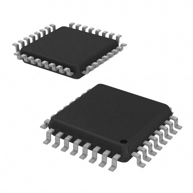
ICGOO电子元器件商城为您提供ADC12081CIVT/NOPB由Texas Instruments设计生产,在icgoo商城现货销售,并且可以通过原厂、代理商等渠道进行代购。 ADC12081CIVT/NOPB价格参考¥45.89-¥76.54。Texas InstrumentsADC12081CIVT/NOPB封装/规格:数据采集 - 模数转换器, 12 Bit Analog to Digital Converter 1 Input 1 Pipelined 32-TQFP (7x7)。您可以下载ADC12081CIVT/NOPB参考资料、Datasheet数据手册功能说明书,资料中有ADC12081CIVT/NOPB 详细功能的应用电路图电压和使用方法及教程。
| 参数 | 数值 |
| 产品目录 | 集成电路 (IC) |
| 描述 | IC ADC 12BIT 5MSPS 32LQFP |
| 产品分类 | |
| 品牌 | Texas Instruments |
| 数据手册 | |
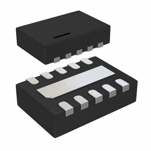
| 产品图片 |
|
| 产品型号 | ADC12081CIVT/NOPB |
| rohs | 无铅 / 符合限制有害物质指令(RoHS)规范要求 |
| 产品系列 | - |
| 位数 | 12 |
| 供应商器件封装 | 32-TQFP(7x7) |
| 其它名称 | *ADC12081CIVT |
| 包装 | 托盘 |
| 安装类型 | 表面贴装 |
| 封装/外壳 | 32-LQFP |
| 工作温度 | -40°C ~ 85°C |
| 数据接口 | 并联 |
| 标准包装 | 250 |
| 特性 | - |
| 电压源 | 模拟和数字 |
| 转换器数 | 1 |
| 输入数和类型 | 1 个单端,单极 |
| 配用 | /product-detail/zh/ADC12081EVAL/ADC12081EVAL-ND/366337 |
| 采样率(每秒) | 5M |




- 商务部:美国ITC正式对集成电路等产品启动337调查
- 曝三星4nm工艺存在良率问题 高通将骁龙8 Gen1或转产台积电
- 太阳诱电将投资9.5亿元在常州建新厂生产MLCC 预计2023年完工
- 英特尔发布欧洲新工厂建设计划 深化IDM 2.0 战略
- 台积电先进制程称霸业界 有大客户加持明年业绩稳了
- 达到5530亿美元!SIA预计今年全球半导体销售额将创下新高
- 英特尔拟将自动驾驶子公司Mobileye上市 估值或超500亿美元
- 三星加码芯片和SET,合并消费电子和移动部门,撤换高东真等 CEO
- 三星电子宣布重大人事变动 还合并消费电子和移动部门
- 海关总署:前11个月进口集成电路产品价值2.52万亿元 增长14.8%




PDF Datasheet 数据手册内容提取
ADC12081 www.ti.com SNAS020D–MARCH2000–REVISEDMARCH2013 ADC12081 12-Bit, 5 MHz Self-Calibrating, Pipelined A/D Converter with Internal Sample & Hold CheckforSamples:ADC12081 FEATURES DESCRIPTION 1 • Single5VPowerSupply The ADC12081 is a monolithic CMOS analog-to- 2 digital converter capable of converting analog input • SimpleAnalogInputInterface signalsinto12-bitdigitalwordsat5megasamplesper • InternalSample-and-Hold second (MSPS). The ADC12081 utilizes an • InternalReferenceBufferAmplifier innovative pipeline architecture to minimize die size and power consumption. The ADC12081 uses self- • LowPowerConsumption calibration and error correction to maintain accuracy andperformanceovertemperature. APPLICATIONS The ADC12081 converter operates on a 5V power • ImageProcessingFrontEnd supply and can digitize analog input signals in the • PC-BasedDataAcquisition range of 0 to 2V. A single convert clock controls the • Scanners conversion operation. All digital I/O is TTL compatible. • FaxMachines The ADC12081 is designed to minimize external • WaveformDigitizer components necessary for the analog input interface. An internal sample-and-hold circuit samples the analog input and an internal amplifier buffers the referencevoltageinput. The ADC12081 is available in the 32-lead LQFP package and is designed to operate over the extended commercial temperature range of -40°C to +85°C. Table1.KeySpecifications VALUE UNIT Resolution 12 Bits ConversionRate 5 Msps(min) DNL ±0.35 LSB(typ) SNR 68 dB(typ) ENOB 10.9 Bits(typ) AnalogInputRange 2 Vpp(min) SupplyVoltage +5±5% V PowerConsumption,5MHz 105 mW(typ) 1 Pleasebeawarethatanimportantnoticeconcerningavailability,standardwarranty,anduseincriticalapplicationsof TexasInstrumentssemiconductorproductsanddisclaimerstheretoappearsattheendofthisdatasheet. Alltrademarksarethepropertyoftheirrespectiveowners. 2 PRODUCTIONDATAinformationiscurrentasofpublicationdate. Copyright©2000–2013,TexasInstrumentsIncorporated Products conform to specifications per the terms of the Texas Instruments standard warranty. Production processing does not necessarilyincludetestingofallparameters.
ADC12081 SNAS020D–MARCH2000–REVISEDMARCH2013 www.ti.com Connection Diagram Simplified Block Diagram 2 SubmitDocumentationFeedback Copyright©2000–2013,TexasInstrumentsIncorporated ProductFolderLinks:ADC12081
ADC12081 www.ti.com SNAS020D–MARCH2000–REVISEDMARCH2013 PINDESCRIPTIONSANDEQUIVALENTCIRCUITS#2 No. Symbol EquivalentCircuit Description Analogsignalinput.Witha2.0Vreferencevoltage,input 2 V signalvoltagesintherangeof0to2.0Voltswillbe IN converted.SeeAnalogInputs. Referencevoltageinput.Thispinshouldbedrivenfroman accurate,stablereferencesourceintherangeof1.8to2.2V 1 V andbypassedtoalow-noiseanaloggroundwithamonolithic REF ceramiccapacitor,nominally0.01µF.SeeReferenceInput. Positivereferencebypasspin.Bypasswitha0.1µF 32 V capacitor.Donotconnectanythingelsetothispin.See RP ReferenceOutputVoltages Referencemidpointbypasspin.Bypasswitha0.1µF 31 V capacitor.Donotconnectanythingelsetothispin.See RM ReferenceOutputVoltages Negativereverencebypasspin.Bypasswitha0.1µF 30 V capacitor.Donotconnectanythingelsetothispin. RN SeeReferenceOutputVoltages SampleClockinput,TTLcompatible.Maximumamplitude 10 CLOCK shouldnotexceed3V. Calibrationrequest,activeHigh.Calibrationcyclestarts 8 CAL whenCALreturnstologiclow.CALisignoredduringpower- downmode.SeeCAL. Power-down,activeHigh,ignoredduringcalibrationcycle. 7 PD SeePDPin Outputenablecontrol,activelow.Whenthispinishighthe 11 OE dataoutputsareinTri-state(high-impedance)mode. Overrangeindicator.ThispinisatalogicHighforV <0or 28 OR IN forV >V . IN REF Devicereadyindicator,activeHigh.ThispinisatalogicLow 29 READY duringacalibrationcycleandwhilethedeviceisinthe powerdownmode. Copyright©2000–2013,TexasInstrumentsIncorporated SubmitDocumentationFeedback 3 ProductFolderLinks:ADC12081
ADC12081 SNAS020D–MARCH2000–REVISEDMARCH2013 www.ti.com PINDESCRIPTIONSANDEQUIVALENTCIRCUITS#2(continued) No. Symbol EquivalentCircuit Description 14-19, Digitaloutputword,CMOScompatible.D0(pin14)isLSB, D0-D11 22-27 D11(pin27)isMSB.Loadwithnomorethan50pF. Analoginputcommon.Connecttoaquietpointinanalog 3 V INcom groundnearthedrivingdevice.SeeLayoutandGrounding. Positiveanalogsupplypin.Connecttoaclean,quietvoltage sourceof+5V.V andV shouldhaveacommonsupply 5 V A D A andbeseparatelybypassedwitha5µFto10µFcapacitor anda0.1µFchipcapacitor. Thegroundreturnfortheanalogsupply.AGNDandDGND 4,6 AGND shouldbeconnectedtogetherclosetotheADC12081 package.SeeLayoutandGrounding. Positiveanalogsupplypin.Connecttoaclean,quietvoltage sourceof+5V.V andV shouldhaveacommonsupply 13 V A D D andbeseparatelybypassedwitha5µFto10µFcapacitor anda0.1µFchipcapacitor. Thegroundreturnfortheanalogsupply.AGNDandDGND 9,12 DGND shouldbeconnectedtogetherclosetotheADC12081 package.SeeLayoutandGrounding Thedigitaloutputdriversupplypin.Thispincanbeoperated 21 V I/O fromasupplyvoltageof3Vto5V,butthevoltageonthispin D shouldneverexceedtheV supplypinvoltage. D Thegroundreturnfortheoutputdrivers.Thispinshouldbe 20 DGNDI/O returnedtoapointinthedigitalgroundthatisremovedfrom theothergroundpinsoftheADC12081. Thesedeviceshavelimitedbuilt-inESDprotection.Theleadsshouldbeshortedtogetherorthedeviceplacedinconductivefoam duringstorageorhandlingtopreventelectrostaticdamagetotheMOSgates. 4 SubmitDocumentationFeedback Copyright©2000–2013,TexasInstrumentsIncorporated ProductFolderLinks:ADC12081
ADC12081 www.ti.com SNAS020D–MARCH2000–REVISEDMARCH2013 Absolute Maximum Ratings(1)(2)(3) SupplyVoltage 6.5V VoltageonAnyOutput −0.3VtoV++0.3V InputCurrentatAnyPin(4) ±25mA PackageInputCurrent(4) ±50mA PackageDissipation See(5) ESDSusceptibility(6) HumanBodyModel 1500V MachineModel 150V SolderingTemp.,Infrared,10sec.(7) 300°C StorageTemp. −65°Cto+150°C MaximumJunctionTemp. 150°C (1) AbsoluteMaximumRatingsindicatelimitsbeyondwhichdamagetothedevicemayoccur.OperatingRatingsindicateconditionsfor whichthedeviceisfunctional,butdonotguaranteespecificperformancelimits.Forguaranteedspecificationsandtestconditions,see theElectricalCharacteristics.Theguaranteedspecificationsapplyonlyforthetestconditionslisted.Someperformancecharacteristics maydegradewhenthedeviceisnotoperatedunderthelistedtestconditions. (2) AllvoltagesaremeasuredwithrespecttoGND=AGND=DGND=0V,unlessotherwisespecified. (3) IfMilitary/Aerospacespecifieddevicesarerequired,pleasecontacttheTISalesOffice/Distributorsforavailabilityandspecifications. (4) Whentheinputvoltageatanypinexceedsthepowersupplies(thatis,V <AGND,orV >V ,V orV I/O),thecurrentatthatpin IN IN A D D shouldbelimitedto25mA.The50mAmaximumpackageinputcurrentratinglimitsthenumberofpinsthatcansafelyexceedthe powersupplieswithaninputcurrentof25mAtotwo. (5) Theabsolutemaximumjunctiontemperatures(Tmax)forthisdeviceis150°C.Themaximumallowablepowerconsumptionisdictated J byTmax,thejunction-to-ambientthermalresistance(θ ),andtheambienttemperature,(T ),andcanbecalculatedusingtheformula J JA A P MAX=(Tmax-T )/θ .Inthe32-pinTQFP,θ is74°C/W,soP MAX=1,689mWat25°Cand1,013mWatthemaximum D J A JA JA D operatingambienttemperatureof75°C.Notethatthepowerconsumptionofthisdeviceundernormaloperationwilltypicallybeabout 125mW(typicalpowerconsumption+20mWTTLoutputloading).Thevaluesformaximumpowerconsumptionlistedabovewillbe reachedonlywhentheADC12081isoperatedinaseverefaultcondition(e.g.wheninputoroutputpinsaredrivenbeyondthepower supplyvoltages,orthepowersupplypolarityisreversed).Obviously,suchconditionsshouldalwaysbeavoided. (6) Humanbodymodelis100pFcapacitordischargedthrougha1.5kΩresistor.Machinemodelis220pfdischargedthroughZEROOhms. (7) SeeAN450,"SurfaceMountingMethodsandTheirEffectonProductReliability",orthesectionentitled"SurfaceMount"foundinany post1986TexasInstrumentsLinearDataBook,forothermethodsofsolderingsurfacemountdevices. Operating Ratings OperatingTemp.Range −40°C≤T ≤+85°C A SupplyVoltage +4.75Vto+5.25V V I/O +2.7VtoV D D V Input 1.8Vto2.2V REF CLOCK,CAL,PD,OE −0.05VtoV +0.05V D |AGND−DGND| ≤100mV Copyright©2000–2013,TexasInstrumentsIncorporated SubmitDocumentationFeedback 5 ProductFolderLinks:ADC12081
ADC12081 SNAS020D–MARCH2000–REVISEDMARCH2013 www.ti.com Converter Electrical Characteristics ThefollowingspecificationsapplyforAGND=DGND=DGNDI/O=0V,V =V =V I/O=+5V,PD=+5V,V =+2.0V, A D D REF f =5MHz,C =50pF/pin.AfterAuto-CalatTemperature.BoldfacelimitsapplyforT =T toT toT :allother CLK L A J MIN MAX limitsT =T =25°C(1)(2)(3) A J Symbol Parameter Conditions Typical(4) Limits(5) Units (Limits) StaticConverterCharacteristics ResolutionwithNoMissingCodes 12 Bits(min) INL IntegralNonLinearity(6) ±0.6 ±1.7 LSB(max) DNL DifferentialNonLinearity ±0.35 ±0.75 LSB(max) Full-ScaleError ±0.05 ±0.1 %FS(max) ZeroError ±0.15 ±0.24 %FS(max) DynamicConverterCharacteristics BW FullPowerBandwidth 100 MHz SNR Signal-to-NoiseRatio f =2.5MHz,V =2.0V 68 65 dB in IN P-P SINAD Signal-to-Noise&Distortion f =2.5MHz,V =2.0V 67.6 64.5 dB in IN P-P ENOB EffectiveNumberofBits f =2.5MHz,V =2.0V 10.9 10.4 Bits in IN P-P THD TotalHamonicDistortion f =2.5MHz,V =2.0V 79 dB in IN P-P SFDR SpuriousFreeDynamicRange f =2.5MHz,V =2.0V 79 dB in IN P-P ReferenceandAnalogInputCharacteristics 0 V(min) V InputVoltageRange V =2.0V IN REF V V(max) REF (CLKLOW) 10 pF C V InputCapacitance V =1.0Vdc+0.7Vrms IN IN IN (CLKHIGH) 15 pF 1.8 V(min) V ReferenceVoltage(7) 2.00 REF 2.2 V(max) ReferenceInputLeakageCurrent 10 µA ReferenceInputResistance 1 MΩ(min) (1) Theinputsareprotectedasshownbelow.Inputvoltagemagnitudesupto5VaboveV orto5VbelowGNDwillnotdamagethisdevice, A providedcurrentislimitedperNote3.However,errorsintheA/DconversioncanoccuriftheinputgoesaboveV orbelowGNDby A morethan100mV.Asanexample,ifV is4.75V,thefull-scaleinputvoltagemustbe≤4.85Vtoensureaccurateconversions. A (2) Toguaranteeaccuracy,itisrequiredthat|V -V |≤100mVandseparatebypassedcapacitorsareusedateachpowersupplypin. A D (3) WiththetestconditionforV =+2.0V,the12-bitLSBis488µV. REF (4) TypicalfiguresareatT =T =25°C,andrepresentmostlikelyparametricnorms. A J (5) TestedlimitsareguaranteedtoTI'sAOQL(AverageOutgoingQualityLevel). (6) IntegralNonLinearityisdefinedasthedeviationoftheanalogvalue,expressedinLSBs,fromthestraightlinethatpassesthrough positivefull-scallandzero. (7) OptimumSNRperformancewillbeobtainedbykeepingthereferenceinputinthe1.8Vto2.2Vrange.TheLM4041CIM3-ADJ(SOT-23 package),theLM4041CIZ-ADJ(TO-92package),ortheLM4041CIM-ADJ(SOT-8package)bandgapvoltagereferenceis recommendedforthisapplication. 6 SubmitDocumentationFeedback Copyright©2000–2013,TexasInstrumentsIncorporated ProductFolderLinks:ADC12081
ADC12081 www.ti.com SNAS020D–MARCH2000–REVISEDMARCH2013 DC and Logic Electrical Characteristics ThefollowingspecificationsapplyforAGND=DGND=DGNDI/O=0V,V =V =V I/O=+5V,PD=+5V,V =+2.0V, A D D REF f =50MHz,C =50pF/pin.AfterAuto-CalatTemperature.BoldfacelimitsapplyforT =T toT ;allotherlimitsT CLK L A MIN MAX A =T =25°C(1)(2)(3) J Symbol Parameter Conditions Typical(4) Limits(5) Units (Limits) CLK,OEDigitalInputCharacteristics V Logical"1"InputVoltage V+=5.25V 2.0 V(min) IH V Logical"0"InputVoltage V+=4.75V 0.8 V(min) IL I Logical"1"InputCurrent V =5.0V 5 µA IH IN I Logical"0"InputCurrent V =0V −5 µA IL IN C V InputCapacitance 8 pF IN IN D0-D11DigitalOutputCharacteristics(6) V Logical"1"OutputVoltage I =−1mA 4 V(min) OH OUT V Logical"0"OutputVoltage I =1.6mA 0.4 V(max) OL OUT I TRI-STATEOutputCurrent V =3Vor5V 10 µA OZ OUT V =0V −10 µA OUT +I OutputShortCircuitSourceCurrent VDDO=3V,V =0V −14 mA(min) SC OUT −I OutputShortCircuitSinkCurrent VDDO=3V,V =V 16 mA(min) SC OUT O PowerSupplyCharacteristics PD=VDDO 2.5 4 mA(max) I AnalogSupplyCurrent A PD=DGND 20 26 mA(max) PD=VDDO 0.5 2 mA(max) I DigitalSupplyCurrent D PD=DGND 1 2 mA(max) PD=VDDO 15 30 mW(max) TotalPowerConsumption PD=DGND 105 140 mW(max) (1) Theinputsareprotectedasshownbelow.Inputvoltagemagnitudesupto5VaboveV orto5VbelowGNDwillnotdamagethisdevice, A providedcurrentislimitedperNote3.However,errorsintheA/DconversioncanoccuriftheinputgoesaboveV orbelowGNDby A morethan100mV.Asanexample,ifV is4.75V,thefull-scaleinputvoltagemustbe≤4.85Vtoensureaccurateconversions. A (2) Toguaranteeaccuracy,itisrequiredthat|V -V |≤100mVandseparatebypassedcapacitorsareusedateachpowersupplypin. A D (3) WiththetestconditionforV =+2.0V,the12-bitLSBis488µV. REF (4) TypicalfiguresareatT =T =25°C,andrepresentmostlikelyparametricnorms. A J (5) TestedlimitsareguaranteedtoTI'sAOQL(AverageOutgoingQualityLevel). (6) TimingspecificationsaretestedattheTTLlogiclevels,V =0.4VforafallingedgeandV =2.4Vforarisingedge.TRI-STATEoutput IL IH voltageisforcedto1.4V. Copyright©2000–2013,TexasInstrumentsIncorporated SubmitDocumentationFeedback 7 ProductFolderLinks:ADC12081
ADC12081 SNAS020D–MARCH2000–REVISEDMARCH2013 www.ti.com AC Electrical Characteristics ThefollowingspecificationsapplyforAGND=DGND=DGNDI/O=0V,V =V =V I/O=+5V,PD=+5V,V =+2.0V, A D D REF f =5MHz,C =50pF/pin.AfterAuto-CalatTemperature.BoldfacelimitsapplyforT =T toT ;allotherlimitsT CLK L A MIN MAX A =T =25°C(1)(2)(3) J Symbol Parameter Conditions Typical(3) Limits(4) Units (Limits) 0.5 MHz(min) f ClockFrequency CLK 5 MHz(max) ClockDutyCycle 50 % t ConversionLatency 10.25 ClockCycles CONV t ApertureDelayTime 3.5 ns AD t V I/O=3V 44 OD D Dataoutputdelayafterrisingclkedge ns V I/O=5V 40 D t DataoutputsintoTristatemode 21 nA(max) DIS t DataoutputsactiveafterTristate 21 ns(max) EN t Calibrationrequestpulsewidth 3 Tclk(min) WCAL t ReadyLowafterCALrequest 3 Tclk RDYC t Calibrationcycle 4000 Tclk CAL t Power-downpulsewidth 3 Tclk(min) WPD t ReadyLowafterPDrequest 3 Tclk RDYPD t Powerdownmodeexitcycle 4000 Tclk PD (1) Theinputsareprotectedasshownbelow.Inputvoltagemagnitudesupto5VaboveV orto5VbelowGNDwillnotdamagethisdevice, A providedcurrentislimitedperNote3.However,errorsintheA/DconversioncanoccuriftheinputgoesaboveV orbelowGNDby A morethan100mV.Asanexample,ifV is4.75V,thefull-scaleinputvoltagemustbe≤4.85Vtoensureaccurateconversions. A (2) Toguaranteeaccuracy,itisrequiredthat|V -V |≤100mVandseparatebypassedcapacitorsareusedateachpowersupplypin. A D (3) TypicalfiguresareatT =T =25°C,andrepresentmostlikelyparametricnorms. A J (4) TestedlimitsareguaranteedtoTI'sAOQL(AverageOutgoingQualityLevel). 8 SubmitDocumentationFeedback Copyright©2000–2013,TexasInstrumentsIncorporated ProductFolderLinks:ADC12081
ADC12081 www.ti.com SNAS020D–MARCH2000–REVISEDMARCH2013 Transfer Characteristic Figure1. TransferCharacteristic Figure2. ErrorsMinimizedbytheAuto-CalCycle Copyright©2000–2013,TexasInstrumentsIncorporated SubmitDocumentationFeedback 9 ProductFolderLinks:ADC12081
ADC12081 SNAS020D–MARCH2000–REVISEDMARCH2013 www.ti.com Typical Performance Characteristics INLvsTemperature DNLvsTemperature Figure3. Figure4. SNRvsTemperature SINADvsTemperature Figure5. Figure6. THDvsTemperature Figure7. 10 SubmitDocumentationFeedback Copyright©2000–2013,TexasInstrumentsIncorporated ProductFolderLinks:ADC12081
ADC12081 www.ti.com SNAS020D–MARCH2000–REVISEDMARCH2013 Specification Definitions APERTURE JITTER is the variation in aperture delay from sample to sample. Aperture jitter shows up as input noise. APERTUREDELAYSeeSamplingDelay. CLOCKDUTYCYCLEistheratioofthetimethattheclockwaveformishightothetotaltimeforoneclockcycle. DIFFERENTIAL NON-LINEARITY (DNL) is the measure of the maximum deviation from the ideal step size of 1 LSB. EFFECTIVE NUMBER OF BITS (ENOB, or EFFECTIVE BITS) is another method of specifying Signal-to-Noise and Distortion Ratio, or SINAD. ENOB is defined as (SINAD - 1.76) / 6.02 and says that the converter is equivalenttoaperfectADCofthis(ENOB)numberofbits. FULL POWER BANDWIDTH is the frequency at which the reconstructed output fundamental drops 3 dB below itslowfrequencyvalueforafullscaleinput. FULL SCALE ERROR is the difference between the input voltage just causing a transition to positive full scale andV -1.5LSB. REF INTEGRAL NON-LINEARITY (INL) is a measure of the deviation of each individual code from a line drawn from negative full scale (½ LSB below the first code transition) through positive full scale (1½ LSB above the last code transition). The deviation of any given code from this straight line is measured from the center of that code value. Theendpointtestmethodisused.INLiscommonlymeasuredatratedclockfrequencywitharampinput. INTERMODULATION DISTORTION (IMD) is the creation of additional spectral components as a result of two sinusoidal frequencies being applied to the ADC input at the same time. It is defined as the ratio of the power in theintermodulationproductstothetotalpowerintheoriginalfrequencies.IMDisusuallyexpressedindB. PIPELINE DELAY (LATENCY) is the number of clock cycles between initiation of conversion and the availability of that conversion result at the output. New data is available at every clock cycle, but the data lags the conversionbythepipelinedelayplustheOutputDelay. SAMPLING (APERTURE) DELAY is the time after the edge of the clock to when the input signal is acquired or heldforconversion. SIGNAL TO NOISE PLUS DISTORTION (S/(N+D) or SINAD) is the ratio expressed in dB, of the rms value of the input signal to the rms value of all of the other spectral components below half the clock frequency, including harmonicsbutexcludingdc. SIGNAL TO NOISE RATIO (SNR) is the ratio of the rms value of the input signal to the rms value of the other spectralcomponentsbelowone-halfthesamplingfrequency,notincludingharmonicsordc. SPURIOUS FREE DYNAMIC RANGE (SFDR) is the difference, expressed in dB, between the rms values of the input signal and the peak spurious signal, where a spurious signal is any signal present in the output spectrum thatisnotpresentattheinput. TOTAL HARMONIC DISTORTION (THD) is the ratio of the rms total of the first six harmonic components, to the rmsvalueoftheinputsignal. ZERO SCALE OFFSET ERROR is the difference between the ideal input voltage (½ LSB) and the actual input voltagethatjustcausesatransitionfromanoutputcodeofzerotoanoutputcodeofone. ZEROERRORseeZeroScaleOffsetError. Copyright©2000–2013,TexasInstrumentsIncorporated SubmitDocumentationFeedback 11 ProductFolderLinks:ADC12081
ADC12081 SNAS020D–MARCH2000–REVISEDMARCH2013 www.ti.com TEST CIRCUIT DIAGRAMS TimingDiagrams Figure8. DataOutputTiming 12 SubmitDocumentationFeedback Copyright©2000–2013,TexasInstrumentsIncorporated ProductFolderLinks:ADC12081
ADC12081 www.ti.com SNAS020D–MARCH2000–REVISEDMARCH2013 Figure9. ResetandCalibrationTiming Copyright©2000–2013,TexasInstrumentsIncorporated SubmitDocumentationFeedback 13 ProductFolderLinks:ADC12081
ADC12081 SNAS020D–MARCH2000–REVISEDMARCH2013 www.ti.com FUNCTIONAL DESCRIPTION The ADC12081 is a monolithic CMOS analog-to-digital converter capable of converting analog input signals into 12-bit digital words at 5 megasamples per second (MSPS). This device utilizes a proprietary pipeline architecture and algorithm to minimize die size and power consumption. The ADC12081 uses self-calibration and digital error correction to maintain accuracy and performance over temperature. The ADC12081 has an input sample-and- hold amplifier and internal reference buffer. The analog input and the reference voltage are converted to differential signals for internal use. Using differential signals in the analog conversion core reduces crosstalk and noisepickupfromthedigitalsectionandpowersupply. The pipeline conversion core has 15 sequential signal processing stages. Each stage receives an analog signal from the previous stage (called “residue” ) and produces a 1-bit digital output that is sent to the digital correction module.Ateachstagetheanalogsignalreceivedfromthepreviousstageiscomparedtoaninternallygenerated reference level. It is then amplified by a factor of 2, and, depending on the output of the comparator, the internal reference signal may be subtracted from the amplifier output. This produces the residue that is passed to the nextstage. The calibration module is activated at power-on or by user request. During calibration the conversion core is put into a special mode of operation in order to determine inherent errors in the analog conversion blocks and to determine correction coefficients for each digital output bit from the conversion core and stores these coefficients in RAM. The digital correction module uses the coefficients in RAM to convert the raw data bits from the conversioncoreintothe12-bitdigitaloutputcode. Applications Information ANALOGINPUTS TheADC12081hastwosingle-endedanaloginputs.V isthereferenceinputandV isthesignalinput. REF IN ReferenceInput The V input must be driven from an accurate, stable reference voltage source. of 1.8V to 2.2V, and bypassed REF toaclean,quietpointinanalogground. AnalogSignalInput The V input must be driven with a low impedance signal source that does not add any distortion to the input IN signal. The ground reference for the V input is the V pin. The V pin must be connected to a clean, IN INCOM INCOM quietpointinanalogground. DIGITALINPUTS TheADC12081hasfourdigitalinputs.TheyareCLOCK,CAL,OEandPD. CLOCK The CLOCK signal drives an internal phase delay loop to create timing for the ADC. The clock input should be driven with a stable, low phase jitter TTL level clock signal in the range of 0.5 to 5 MHz. The trace carrying the clock signal should be as short as possible. This trace should not cross any other signal line, analog or digital, not even at 90°. A 100 Ohm resistor should be placed in series with the CLOCK pin, as close to the pin as possible. CAL The level sensitive CAL input must be pulsed high for at least three clock cycles to begin ADC calibration. For best performance, calibration should be performed about ten seconds after power up, after resetting the ADC, andafterthetemperaturehaschangedbymorethan50°Csincethelastcalibrationwasperformed. Calibration should be performed at the same clock frequency that the ADC12081 will be used for conversions to minimizeoffseterrors.Calibrationtakes4000clockcycles.IrrelevantdatamayappearduringCAL. 14 SubmitDocumentationFeedback Copyright©2000–2013,TexasInstrumentsIncorporated ProductFolderLinks:ADC12081
ADC12081 www.ti.com SNAS020D–MARCH2000–REVISEDMARCH2013 OEPin The OE pin is used to control the state of the outputs. When the OE pin is low, the output buffers go into the activestate.WhentheOEinputishigh,theoutputbuffersareinthehighimpedancestate. PDPin The PD pin, when high, holds the ADC12081 in a power-down mode where power consumption is typically less than 15 mW to conserve power when the converter is not being used. The ADC12081 will begin normal operation within t after this pin is brought low, provided a valid CLOCK input is present. The data in the PD pipeline is corrupted while in the power down mode. The ADC12081 should be re-calibrated after a power-down cycletoensureoptimumperformance. OUTPUTS The ADC12081 has three analog outputs: reference output voltages V , V , and V . There are 14 digital RN RM RP outputs:12DataOutputpins,ReadyandOR(Outofrange). ReferenceOutputVoltages The reference output voltages are made available only for the purpose of bypassing with capacitors to a clean analogground.Therecommendedbypasscapacitorsare0.1µFceramicchipcapacitors.Donotloadthesepins. ReadyOutput The Ready output goes high to indicate that the converter is ready for operation. This signal will go low when the converterisCalibrationorPowerDownmade. OR(OutofRange)Output The OR output goes high when the analog input is below GND or above V . This output is low when the input REF signalisinthevalidrangeofoperation(0V≤ V ≤ V ). IN REF DataOutputs TheDataOutputsareTTL/CMOScompatible.Theoutputdataformatis12bitsstraightbinary. Minimizing the digital output currents will help to minimize noise due to output switching. This can be done by connecting buffers between the ADC outputs and any other circuitry. Only one buffer input should be connected to each output. Additionally, inserting series resistors of 47 to 56 Ohms right at the digital outputs, close to the ADCpins,willisolatetheoutputsfromothercircuitryandlimitoutputcurrents. POWERSUPPLYCONSIDERATIONS Each power pin should be bypassed with a parallel combination of a 10µF capacitor and a 0.1µF ceramic chip capacitor. The chip capacitors should be within 1/2 centimeter of the power pins. Leadless chip capacitors are preferredbecausetheyprovidelowleadinductance. The converter's digital logic supply (V ) should be well isolated from the supply that is used for other digital D circuitry on the board. A common power supply should be used for both V (analog supply) and V (digital A D supply), and each of these supply pins should be separately bypassed with a 0.1µF ceramic capacitor and a low ESR 10µF electrolytic capacitor. A ferrite bead or inductor should be used between V and V to prevent noise A D couplingfromthedigitalsupplyintotheanalogcircuit. V I/Oisthepowerpinfortheoutputdriver.Thispinmaybesuppliedwithapotentialbetween2.7VandV .This D D makes it easy to interface the ADC12081 with 3V or 5V logic families. Powering the V I/O from 3 Volts will also D reduce power consumption and noise generation due to output switching. DO NOT operate the V I/O at a D voltagehigherthanV orV !Allpowersuppliesconnectedtothedeviceshouldbeappliedsimultaneously. D A As is the case with all high speed converters, the ADC12081 is sensitive to power supply noise. Accordingly, the noiseontheanalogsupplypinshouldbeminimized,keepingitbelow100mVP-P. Copyright©2000–2013,TexasInstrumentsIncorporated SubmitDocumentationFeedback 15 ProductFolderLinks:ADC12081
ADC12081 SNAS020D–MARCH2000–REVISEDMARCH2013 www.ti.com Figure10. BasicConnectionsDiagram LAYOUTANDGROUNDING Proper grounding and routing of all signals is essential to ensure accurate conversion. Separate analog and digital ground planes that are connected beneath the ADC12081 are required to achieve specified performance. The analog and digital grounds may be in the same layer, but should be separated from each other and should neveroverlapeachother.Separationshouldbeatleast1/8inch,wherepossible. The ground return for the output buffer digital supply (DGND I/O) carries the ground current for the output drivers. This pin should be connected to the system digital ground. The current on this pin can exhibit high transients that could add noise to the conversion process. To prevent this from happening, the DGND I/O pin shouldNOTbeconnectedincloseproximitytoanyoftheADC12081'sothergroundpins.SeeFigure11. Capacitive coupling between the typically noisy digital ground plane and the sensitive analog circuitry can lead to poor performance that may seem impossible to isolate and remedy. The solution is to keep the analog circuitry separatedfromthedigitalcircuitryandfromthedigitalgroundplane. Digital circuits create substantial supply and ground current transients. The logic noise thus generated could have significant impact upon system noise performance. The best logic family to use in systems with A/D converters is one which employs non-saturating transistor designs, or has low noise characteristics, such as the 74LS, 74HC(T) and 74 AC(T)Q families. The worst noise generators are logic families that draw the largest supplycurrenttransientsduringclockorsignaledges,likethe74Fandthe74AC(T)families. Since digital switching transients are composed largely of high frequency components, total ground plane copper weight will have little effect upon the logic-generated noise. This is because of the skin effect. Total surface area ismoreimportantthanistotalgroundplanevolume. 16 SubmitDocumentationFeedback Copyright©2000–2013,TexasInstrumentsIncorporated ProductFolderLinks:ADC12081
ADC12081 www.ti.com SNAS020D–MARCH2000–REVISEDMARCH2013 An effective way to control ground noise is by connecting the analog and digital ground planes together beneath the ADC with a copper trace that is very narrow compared with the rest of the ground plane. This narrowing beneath the converter provides a fairly high impedance to the high frequency components of the digital switching currents, directing them away from the analog pins. The relatively lower frequency analog ground currents do not createasignificantvoltagedropacrosstheimpedanceofthisnarrowgroundconnection. To maximize accuracy in high speed, high resolution systems, avoid crossing analog and digital signal traces. It is important to keep any clock lines isolated from ALL other lines. Even the generally accepted 90 degree crossing should be avoided as even a little coupling can cause problems at high frequencies. This is because otherlinescanintroducephasenoise(jitter)intotheclockline,whichcanleadtodegradationofSNR. Best performance at high frequencies and at high resolution is obtained with a straight signal path. That is, the signalpaththroughallcomponentsshouldformastraightlinewhereverpossible. Be especially careful with the layout of inductors. Mutual inductance can change the characteristics of the circuit in which they are used. Inductors should not be placed side by side, even with just a small part of their bodies besideeachother. The analog input should be isolated from noisy signal traces to avoid coupling of spurious signals into the input. Any external component (e.g., a filter capacitor) connected between the converter's input and ground should be connectedtoaverycleanpointintheanaloggroundplane. Figure11. Layoutexample Figure 11 gives an example of a suitable layout. All analog circuitry (input amplifiers, filters, reference components, etc.) should be placed on or over the analog ground plane. All digital circuitry and I/O lines should beplacedoverthedigitalgroundplane. Allgroundconnectionsshouldhavealowinductancepathtoground. LAYOUTANDGROUNDING The ADC12081 can achieve impressive dynamic performance. To achieve the best dynamic performance with the ADC12081, the clock source driving the CLK input must be free of jitter. For best ac performance, isolating the ADC clock from any digital circuitry should be done with adequate buffers, as with a clock tree. See Figure12. Copyright©2000–2013,TexasInstrumentsIncorporated SubmitDocumentationFeedback 17 ProductFolderLinks:ADC12081
ADC12081 SNAS020D–MARCH2000–REVISEDMARCH2013 www.ti.com Figure12. IsolatingtheADCclockfromothercircuitrywithaclocktree. It is good practice to keep the ADC clock line as short as possible and to keep it well away from any other signals. Other signals can introduce phase noise (jitter) into the clock signal, which can lead to increased distortion. Even lines with 90° crossings have capacitive coupling, so try to avoid even these 90° crossings of the clockline. COMMONAPPLICATIONPITFALLS Driving the inputs (analog or digital) beyond the power supply rails. For proper operation, all inputs should not go more than 300mV beyond the supply rails (more than 300mV below the ground pins or 300mV above the supply pins). Exceeding these limits on even a transient basis may cause faulty or erratic operation. It is not uncommonforhighspeeddigitalcircuits(e.g.,74Fand74ACdevices) to exhibit undershoot that goes more than a volt below ground above the power supply. A resistor of about 50 to 100Ω in series with the offending digital inputwilleliminatetheproblem. Care should be taken not to overdrive the inputs of the ADC12081 with a device that is powered from supplies outside the range of the ADC12081 supply. Such practice may lead to conversion inaccuracies and even to devicedamage. Attempting to drive a high capacitance digital data bus. Capacitive loading on the digital outputs causes instantaneous digital currents to flow from the V I/O supply into the DGND I/O ground plane. These large D charging current spikes can couple into the analog section, degrading dynamic performance. Adequate bypassing and maintaining separate analog and digital ground planes will reduce this problem. The digital data outputs should be buffered (with 74ACQ541, for example). Dynamic performance can also be improved by adding series resistors at each digital output, close to the ADC12081, reducing the energy coupled back into the converteroutputpinsbylimitingtheoutputslewrate.Areasonablevaluefortheseresistorsis47Ω. Using an inadequate amplifier to drive the analog input. The analog input circuits of the ADC12081 place a switched capacitor load on the input signal source. Therefore the amplifier used to drive the ADC12081 must havealowimpedanceoutputandadequatebandwidthtoavoiddistortionoftheinputsignal. Operating with the reference pins outside of the specified range. As mentioned in Analog Inputs, V REF shouldbeintherangeof1.8V≤ V ≤ 2.2V.Operatingoutsideoftheselimitscouldleadtosignaldistortion. REF Using a clock source with excessive jitter, using excessively long clock signal trace, or having other signals coupled to the clock signal trace. This will cause the sampling interval to vary, causing excessive outputnoiseandareductioninSNRperformance. 18 SubmitDocumentationFeedback Copyright©2000–2013,TexasInstrumentsIncorporated ProductFolderLinks:ADC12081
ADC12081 www.ti.com SNAS020D–MARCH2000–REVISEDMARCH2013 REVISION HISTORY ChangesfromRevisionC(March2013)toRevisionD Page • ChangedlayoutofNationalDataSheettoTIformat.......................................................................................................... 18 Copyright©2000–2013,TexasInstrumentsIncorporated SubmitDocumentationFeedback 19 ProductFolderLinks:ADC12081
PACKAGE OPTION ADDENDUM www.ti.com 6-Feb-2020 PACKAGING INFORMATION Orderable Device Status Package Type Package Pins Package Eco Plan Lead/Ball Finish MSL Peak Temp Op Temp (°C) Device Marking Samples (1) Drawing Qty (2) (6) (3) (4/5) ADC12081CIVT/NOPB ACTIVE LQFP NEY 32 250 Green (RoHS SN Level-3-260C-168 HR -20 to 75 ADC12081 & no Sb/Br) CIVT ADC12081CIVTX/NOPB ACTIVE LQFP NEY 32 1000 Green (RoHS SN Level-3-260C-168 HR -20 to 75 ADC12081 & no Sb/Br) CIVT (1) The marketing status values are defined as follows: ACTIVE: Product device recommended for new designs. LIFEBUY: TI has announced that the device will be discontinued, and a lifetime-buy period is in effect. NRND: Not recommended for new designs. Device is in production to support existing customers, but TI does not recommend using this part in a new design. PREVIEW: Device has been announced but is not in production. Samples may or may not be available. OBSOLETE: TI has discontinued the production of the device. (2) RoHS: TI defines "RoHS" to mean semiconductor products that are compliant with the current EU RoHS requirements for all 10 RoHS substances, including the requirement that RoHS substance do not exceed 0.1% by weight in homogeneous materials. Where designed to be soldered at high temperatures, "RoHS" products are suitable for use in specified lead-free processes. TI may reference these types of products as "Pb-Free". RoHS Exempt: TI defines "RoHS Exempt" to mean products that contain lead but are compliant with EU RoHS pursuant to a specific EU RoHS exemption. Green: TI defines "Green" to mean the content of Chlorine (Cl) and Bromine (Br) based flame retardants meet JS709B low halogen requirements of <=1000ppm threshold. Antimony trioxide based flame retardants must also meet the <=1000ppm threshold requirement. (3) MSL, Peak Temp. - The Moisture Sensitivity Level rating according to the JEDEC industry standard classifications, and peak solder temperature. (4) There may be additional marking, which relates to the logo, the lot trace code information, or the environmental category on the device. (5) Multiple Device Markings will be inside parentheses. Only one Device Marking contained in parentheses and separated by a "~" will appear on a device. If a line is indented then it is a continuation of the previous line and the two combined represent the entire Device Marking for that device. (6) Lead/Ball Finish - Orderable Devices may have multiple material finish options. Finish options are separated by a vertical ruled line. Lead/Ball Finish values may wrap to two lines if the finish value exceeds the maximum column width. Important Information and Disclaimer:The information provided on this page represents TI's knowledge and belief as of the date that it is provided. TI bases its knowledge and belief on information provided by third parties, and makes no representation or warranty as to the accuracy of such information. Efforts are underway to better integrate information from third parties. TI has taken and continues to take reasonable steps to provide representative and accurate information but may not have conducted destructive testing or chemical analysis on incoming materials and chemicals. TI and TI suppliers consider certain information to be proprietary, and thus CAS numbers and other limited information may not be available for release. In no event shall TI's liability arising out of such information exceed the total purchase price of the TI part(s) at issue in this document sold by TI to Customer on an annual basis. Addendum-Page 1
PACKAGE OPTION ADDENDUM www.ti.com 6-Feb-2020 Addendum-Page 2
PACKAGE MATERIALS INFORMATION www.ti.com 27-Nov-2015 TAPE AND REEL INFORMATION *Alldimensionsarenominal Device Package Package Pins SPQ Reel Reel A0 B0 K0 P1 W Pin1 Type Drawing Diameter Width (mm) (mm) (mm) (mm) (mm) Quadrant (mm) W1(mm) ADC12081CIVTX/NOPB LQFP NEY 32 1000 330.0 16.4 9.3 9.3 2.2 12.0 16.0 Q2 PackMaterials-Page1
PACKAGE MATERIALS INFORMATION www.ti.com 27-Nov-2015 *Alldimensionsarenominal Device PackageType PackageDrawing Pins SPQ Length(mm) Width(mm) Height(mm) ADC12081CIVTX/NOPB LQFP NEY 32 1000 367.0 367.0 38.0 PackMaterials-Page2
PACKAGE OUTLINE NEY0032A LQFP - 1.6 mm max height SCALE 1.800 PLASTIC QUAD FLATPACK 7.1 B 6.9 32 25 PIN 1 ID 1 24 7.1 9.4 TYP 6.9 8.6 8 17 A 9 16 32X 0.27 28X 0.8 OPTIONAL: 0.17 SHARP CORNERS EXCEPT 0.2 C A B 4X 5.6 PIN 1 ID CORNER SEE DETAIL A 1.6 MAX C SEATING PLANE 0.09-0.20 TYP 0.25 (1.4) GAGE PLANE 0.1 0.15 0.75 0.05 0 -7 0.45 DETSDCEATLAEIL: 1A2AIL A TYPICAL 4219901/A 10/2016 NOTES: 1. All linear dimensions are in millimeters. Any dimensions in parenthesis are for reference only. Dimensioning and tolerancing per ASME Y14.5M. 2. This drawing is subject to change without notice. 3. Reference JEDEC registration MS-026. www.ti.com
EXAMPLE BOARD LAYOUT NEY0032A LQFP - 1.6 mm max height PLASTIC QUAD FLATPACK SYMM 32 25 32X (1.6) 1 24 32X (0.4) SYMM 28X (0.8) (8.5) 8 17 (R0.05) TYP 9 16 (8.5) LAND PATTERN EXAMPLE SCALE:8X 0.07 MAX 0.07 MIN ALL AROUND ALL AROUND METAL SOLDER MASK SOLDER MASK METAL UNDER OPENING SOLDER MASK NON SOLDER MASK SOLDER MASK DEFINED DEFINED SOLDER MASK DETAILS 4219901/A 10/2016 NOTES: (continued) 4. Publication IPC-7351 may have alternate designs. 5. Solder mask tolerances between and around signal pads can vary based on board fabrication site. www.ti.com
EXAMPLE STENCIL DESIGN NEY0032A LQFP - 1.6 mm max height PLASTIC QUAD FLATPACK SYMM 32 25 32X (1.6) 1 24 32X (0.4) SYMM 28X (0.8) (8.5) 8 17 (R0.05) TYP 9 16 (8.5) SOLDER PASTE EXAMPLE SCALE 8X 4219901/A 10/2016 NOTES: (continued) 6. Laser cutting apertures with trapezoidal walls and rounded corners may offer better paste release. IPC-7525 may have alternate design recommendations. 7. Board assembly site may have different recommendations for stencil design. www.ti.com
IMPORTANTNOTICEANDDISCLAIMER TI PROVIDES TECHNICAL AND RELIABILITY DATA (INCLUDING DATASHEETS), DESIGN RESOURCES (INCLUDING REFERENCE DESIGNS), APPLICATION OR OTHER DESIGN ADVICE, WEB TOOLS, SAFETY INFORMATION, AND OTHER RESOURCES “AS IS” AND WITH ALL FAULTS, AND DISCLAIMS ALL WARRANTIES, EXPRESS AND IMPLIED, INCLUDING WITHOUT LIMITATION ANY IMPLIED WARRANTIES OF MERCHANTABILITY, FITNESS FOR A PARTICULAR PURPOSE OR NON-INFRINGEMENT OF THIRD PARTY INTELLECTUAL PROPERTY RIGHTS. These resources are intended for skilled developers designing with TI products. You are solely responsible for (1) selecting the appropriate TI products for your application, (2) designing, validating and testing your application, and (3) ensuring your application meets applicable standards, and any other safety, security, or other requirements. These resources are subject to change without notice. TI grants you permission to use these resources only for development of an application that uses the TI products described in the resource. Other reproduction and display of these resources is prohibited. No license is granted to any other TI intellectual property right or to any third party intellectual property right. TI disclaims responsibility for, and you will fully indemnify TI and its representatives against, any claims, damages, costs, losses, and liabilities arising out of your use of these resources. TI’s products are provided subject to TI’s Terms of Sale (www.ti.com/legal/termsofsale.html) or other applicable terms available either on ti.com or provided in conjunction with such TI products. TI’s provision of these resources does not expand or otherwise alter TI’s applicable warranties or warranty disclaimers for TI products. Mailing Address: Texas Instruments, Post Office Box 655303, Dallas, Texas 75265 Copyright © 2020, Texas Instruments Incorporated

 Datasheet下载