ICGOO在线商城 > 集成电路(IC) > 数据采集 - 模数转换器 > ADC0820CCN/NOPB

 Datasheet下载
- 型号: ADC0820CCN/NOPB
- 制造商: Texas Instruments
- 库位|库存: xxxx|xxxx
- 要求:
| 数量阶梯 | 香港交货 | 国内含税 |
| +xxxx | $xxxx | ¥xxxx |
查看当月历史价格
查看今年历史价格
ADC0820CCN/NOPB产品简介:
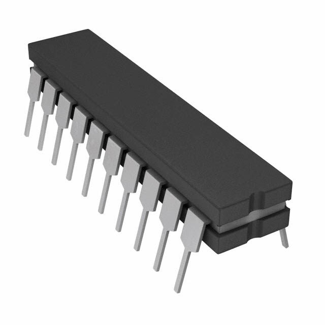
ICGOO电子元器件商城为您提供ADC0820CCN/NOPB由Texas Instruments设计生产,在icgoo商城现货销售,并且可以通过原厂、代理商等渠道进行代购。 ADC0820CCN/NOPB价格参考。Texas InstrumentsADC0820CCN/NOPB封装/规格:数据采集 - 模数转换器, 8 Bit Analog to Digital Converter 1 Input 1 Flash 20-DIP。您可以下载ADC0820CCN/NOPB参考资料、Datasheet数据手册功能说明书,资料中有ADC0820CCN/NOPB 详细功能的应用电路图电压和使用方法及教程。
| 参数 | 数值 |
| 产品目录 | 集成电路 (IC)半导体 |
| 描述 | IC ADC 8BIT MPU COMPAT HS 20-DIP模数转换器 - ADC 8B Hi Spd Compatible A/D Cnvtr |
| 产品分类 | |
| 品牌 | Texas Instruments |
| 产品手册 | |
| 产品图片 |
|
| rohs | 符合RoHS无铅 / 符合限制有害物质指令(RoHS)规范要求 |
| 产品系列 | 数据转换器IC,模数转换器 - ADC,Texas Instruments ADC0820CCN/NOPB- |
| 数据手册 | http://www.ti.com/lit/pdf/snas529c |
| 产品型号 | ADC0820CCN/NOPB |
| 产品 | ADC |
| 产品种类 | 模数转换器 - ADC |
| 位数 | 8 |
| 供应商器件封装 | 20-DIP |
| 信噪比 | Yes |
| 其它名称 | *ADC0820CCN/NOPB |
| 分辨率 | 8 bit |
| 包装 | 管件 |
| 商标 | Texas Instruments |
| 安装类型 | 通孔 |
| 安装风格 | Through Hole |
| 封装 | Tube |
| 封装/外壳 | 20-DIP(0.300",7.62mm) |
| 封装/箱体 | MDIP |
| 工作温度 | 0°C ~ 70°C |
| 工作电源电压 | 5 V |
| 工厂包装数量 | 18 |
| 接口类型 | Parallel |
| 数据接口 | 并联 |
| 最大功率耗散 | 875 mW |
| 最大工作温度 | + 70 C |
| 最小工作温度 | 0 C |
| 标准包装 | 18 |
| 特性 | - |
| 电压参考 | External |
| 电压源 | 单电源 |
| 系列 | ADC0820-N |
| 结构 | Half-Flash |
| 转换器数 | 1 |
| 转换器数量 | 1 |
| 转换速率 | 667 kS/s |
| 输入数和类型 | 1 个单端,单极 |
| 输入类型 | Single-Ended |
| 通道数量 | 1 Channel |
| 采样率(每秒) | - |


- 商务部:美国ITC正式对集成电路等产品启动337调查
- 曝三星4nm工艺存在良率问题 高通将骁龙8 Gen1或转产台积电
- 太阳诱电将投资9.5亿元在常州建新厂生产MLCC 预计2023年完工
- 英特尔发布欧洲新工厂建设计划 深化IDM 2.0 战略
- 台积电先进制程称霸业界 有大客户加持明年业绩稳了
- 达到5530亿美元!SIA预计今年全球半导体销售额将创下新高
- 英特尔拟将自动驾驶子公司Mobileye上市 估值或超500亿美元
- 三星加码芯片和SET,合并消费电子和移动部门,撤换高东真等 CEO
- 三星电子宣布重大人事变动 还合并消费电子和移动部门
- 海关总署:前11个月进口集成电路产品价值2.52万亿元 增长14.8%


PDF Datasheet 数据手册内容提取
ADC0820-N www.ti.com SNAS529C–JUNE1999–REVISEDMARCH2013 ADC0820-N 8-Bit High Speed µP Compatible A/D Converter with Track/Hold Function CheckforSamples:ADC0820-N FEATURES KEY SPECIFICATIONS 1 • Built-InTrack-and-HoldFunction • Resolution:8Bits 2 • NoMissingCodes • ConversionTime • NoExternalClocking – 2.5µsMax(RDMode) • SingleSupply—5V – 1.5µsMax(WR-RDMode) DC • EasyInterfacetoAllMicroprocessors,or • LowPower:75mWMax OperatesStand-Alone • TotalUnadjustedError:±½LSBand ±1LSB • LatchedTRI-STATEOutput DESCRIPTION • LogicInputsandOutputsMeetBothMOSand T2LVoltageLevelSpecifications By using a half-flash conversion technique, the 8-bit ADC0820-N CMOS A/D offers a 1.5 µs conversion • OperatesRatiometricallyorwithany time and dissipates only 75 mW of power. The half- ReferenceValueEqualtoorLessthanV CC flash technique consists of 32 comparators, a most • 0Vto5VAnalogInputVoltageRangewith significant 4-bit ADC and a least significant 4-bit Single5VSupply ADC. • NoZeroorFull-ScaleAdjustRequired The input to the ADC0820-N is tracked and held by • OverflowOutputAvailableforCascading the input sampling circuitry eliminating the need for • 0.3in.StandardWidth20-PinPDIP an external sample-and-hold for signals moving at lessthan100mV/µs. • 20-PinPLCC For ease of interface to microprocessors, the • 20-PinSOIC ADC0820-N has been designed to appear as a memory location or I/O port without the need for externalinterfacinglogic. Connection and Functional Diagrams Figure1.CDIP,PDIP, Figure2.PLCCPackage andSOICPackages(TopView) 1 Pleasebeawarethatanimportantnoticeconcerningavailability,standardwarranty,anduseincriticalapplicationsof TexasInstrumentssemiconductorproductsanddisclaimerstheretoappearsattheendofthisdatasheet. Alltrademarksarethepropertyoftheirrespectiveowners. 2 PRODUCTIONDATAinformationiscurrentasofpublicationdate. Copyright©1999–2013,TexasInstrumentsIncorporated Products conform to specifications per the terms of the Texas Instruments standard warranty. Production processing does not necessarilyincludetestingofallparameters.
ADC0820-N SNAS529C–JUNE1999–REVISEDMARCH2013 www.ti.com Figure3. FunctionalDiagram Thesedeviceshavelimitedbuilt-inESDprotection.Theleadsshouldbeshortedtogetherorthedeviceplacedinconductivefoam duringstorageorhandlingtopreventelectrostaticdamagetotheMOSgates. Absolute Maximum Ratings(1)(2)(3) SupplyVoltage(V ) 10V CC LogicControlInputs −0.2VtoV +0.2V CC VoltageatOtherInputsandOutput −0.2VtoV +0.2V CC StorageTemperatureRange −65°Cto+150°C PackageDissipationatT =25°C 875mW A InputCurrentatAnyPin(4) 1mA PackageInputCurrent(4) 4mA ESDSusceptibility(5) 900V PDIPPackage 260°C CDIPPackage 300°C LeadTemp.(Soldering,10sec.) VaporPhase(60sec.) 215°C SOICPackage Infrared(15sec.) 220°C (1) AbsoluteMaximumRatingsindicatelimitsbeyondwhichdamagetothedevicemayoccur.DCandACelectricalspecificationsdonot applywhenoperatingthedevicebeyonditsspecifiedoperatingconditions. (2) AllvoltagesaremeasuredwithrespecttotheGNDpin,unlessotherwisespecified. (3) IfMilitary/Aerospacespecifieddevicesarerequired,pleasecontacttheTexasInstrumentsSalesOffice/Distributorsforavailabilityand specifications. (4) Whentheinputvoltage(V )atanypinexceedsthepowersupplyrails(V <V−orV >V+)theabsolutevalueofcurrentatthatpin IN IN IN shouldbelimitedto1mAorless.The4mApackageinputcurrentlimitsthenumberofpinsthatcanexceedthepowersupply boundarieswitha1mAcurrentlimittofour. (5) Humanbodymodel,100pFdischargedthrougha1.5kΩresistor. Operating Ratings(1)(2) ADC0820CCJ,ADC0820CIWM −40°C≤T ≤+85°C A TemperatureRange(TMIN≤TA≤TMAX) ADC0820BCN,ADC0820CCN,ADC0820BCV, 0°C≤T ≤70°C ADC0820BCWM,ADC0820CCWM A V Range 4.5Vto8V CC (1) AbsoluteMaximumRatingsindicatelimitsbeyondwhichdamagetothedevicemayoccur.DCandACelectricalspecificationsdonot applywhenoperatingthedevicebeyonditsspecifiedoperatingconditions. (2) AllvoltagesaremeasuredwithrespecttotheGNDpin,unlessotherwisespecified. 2 SubmitDocumentationFeedback Copyright©1999–2013,TexasInstrumentsIncorporated ProductFolderLinks:ADC0820-N
ADC0820-N www.ti.com SNAS529C–JUNE1999–REVISEDMARCH2013 Converter Characteristics ThefollowingspecificationsapplyforRDmode(pin7=0),V =5V,V (+)=5V,andV (−)=GNDunlessotherwise CC REF REF specified.BoldfacelimitsapplyfromT toT ;allotherlimitsT =T =25°C. MIN MAX A j ADC0820BCN,ADC0820CCN, ADC0820CCJ ADC0820BCV,ADC0820BCWM, Parameter Conditions ADC0820CCWM,ADC0820CIWM Limit Units Typ(1) LTiemsitte(d2) LDiemsiitg(3n) Typ(1) LTiemsitte(d2) LDiemsiitg(3n) Resolution 8 8 8 Bits ADC0820BCN,BCWM ±½ ±½ LSB TotalUnadjusted ADC0820CCJ ±1 LSB Error(4) ADC0820CCN,CCWM,CIWM ±1 ±1 LSB ADC0820CCMSA ±1 ±1 LSB MinimumReference 2.3 1.00 2.3 1.2 kΩ Resistance MaximumReference 2.3 6 2.3 5.3 6 kΩ Resistance MaximumV (+) REF V V V V InputVoltage CC CC CC MinimumV (−) REF GND GND GND V InputVoltage MinimumV (+) REF V (−) V (−) V (−) V InputVoltage REF REF REF MaximumV (−) REF V (+) V (+) V (+) V InputVoltage REF REF REF MaximumV Input IN V +0.1 V +0.1 V +0.1 V Voltage CC CC CC MinimumV Input IN GND−0.1 GND−0.1 GND−0.1 V Voltage CS=V MaximumAnalog CC InputLeakage V =V 3 0.3 3 µA IN CC Current V =GND −3 −0.3 −3 µA IN PowerSupply V =5V±5% ±1/16 ±¼ ±1/16 ±¼ ±¼ LSB Sensitivity CC (1) Typicalsareat25°Candrepresentmostlikelyparametricnorm. (2) TestedlimitsareensuredtoTI'sAOQL(AverageOutgoingQualityLevel). (3) Designlimitsarespecifiedbutnot100%tested.Theselimitsarenotusedtocalculateoutgoingqualitylevels. (4) Totalunadjustederrorincludesoffset,full-scale,andlinearityerrors. Copyright©1999–2013,TexasInstrumentsIncorporated SubmitDocumentationFeedback 3 ProductFolderLinks:ADC0820-N
ADC0820-N SNAS529C–JUNE1999–REVISEDMARCH2013 www.ti.com DC Electrical Characteristics ThefollowingspecificationsapplyforV =5V,unlessotherwisespecified.BoldfacelimitsapplyfromT toT ;all CC MIN MAX otherlimitsT =T =25°C. A J ADC0820BCN,ADC0820CCN, ADC0820CCJ ADC0820BCV,ADC0820BCWM, Parameter Conditions ADC0820CCWM,ADC0820CIWM Limit Units Typ(1) LTiemsitte(d2) LDiemsiitg(3n) Typ(1) LTiemsitte(d2) LDiemsiitg(3n) V ,Logical“1” CS,WR,RD 2.0 2.0 2.0 V IN(1) V =5.25V InputVoltage CC Mode 3.5 3.5 3.5 V V ,Logical“0” CS,WR,RD 0.8 0.8 0.8 V IN(0) V =4.75V InputVoltage CC Mode 1.5 1.5 1.5 V V =5V;CS,RD 0.005 1 0.005 1 µA IN(1) I ,Logical“1” IN(1) V =5V;WR 0.1 3 0.1 0.3 3 µA InputCurrent IN(1) V =5V;Mode 50 200 50 170 200 µA IN(1) I ,Logical“0” V =0V;CS,RD,WR,Mode IN(0) IN(0) −0.005 −1 −0.005 −1 µA InputCurrent V =4.75V,I =−360µA; CC OUT 2.4 2.8 2.4 V V ,Logical“1” DB0–DB7,OFL,INT OUT(1) OutputVoltage V =4.75V,I =−10µA; CC OUT 4.5 4.6 4.5 V DB0–DB7,OFL,INT V ,Logical“0” V =4.75V,I =1.6mA; OUT(0) CC OUT 0.4 0.34 0.4 V OutputVoltage DB0–DB7,OFL,INT,RDY IOUT,TRI-STATE VOUT=5V;DB0–DB7,RDY 0.1 3 0.1 0.3 3 µA OutputCurrent V =0V;DB0–DB7,RDY −0.1 −3 −0.1 −0.3 −3 µA OUT ISOURCE,Output VOUT=0V;DB0–DB7,OFL −12 −6 −12 −7.2 −6 mA SourceCurrent INT −9 −4.0 −9 −5.3 −4.0 mA I ,OutputSink V =5V;DB0–DB7,OFL, SINK OUT 14 7 14 8.4 7 mA Current INT,RDY I ,SupplyCurrent CS=WR=RD=0 7.5 15 7.5 13 15 mA CC (1) Typicalsareat25°Candrepresentmostlikelyparametricnorm. (2) TestedlimitsareensuredtoTI'sAOQL(AverageOutgoingQualityLevel). (3) Designlimitsarespecifiedbutnot100%tested.Theselimitsarenotusedtocalculateoutgoingqualitylevels. 4 SubmitDocumentationFeedback Copyright©1999–2013,TexasInstrumentsIncorporated ProductFolderLinks:ADC0820-N
ADC0820-N www.ti.com SNAS529C–JUNE1999–REVISEDMARCH2013 AC Electrical Characteristics ThefollowingspecificationsapplyforV =5V,t =t =20ns,V (+)=5V,V (−)=0VandT =25°Cunlessotherwise CC r f REF REF A specified. Parameter Conditions Typ(1) LTiemsitte(d2) LDiemsiitg(3n) Units t ,ConversionTimeforRDMode Pin7=0(Figure4) 1.6 2.5 µs CRD t ,AccessTime(DelayfromFalling ACC0 Pin7=0(Figure4) t +20 t +50 ns EdgeofRDtoOutputValid) CRD CRD t ,ConversionTimeforWR-RD Pin7=V ;t =600ns,t =600ns CWR-RD CC WR RD 1.52 µs Mode (Figure5&Figure6) Min Pin7=V (Figure5&Figure6) 600 ns CC t ,WriteTime WR Max Figure11(4) 50 µs Pin7=V (Figure5&Figure6& tRD,ReadTime Min Figure12C)(C4) 600 ns tACC1,AccessTime(DelayfromFalling Pin7=VCC,tRD<tI,CL=15pF(Figure5) 190 280 ns EdgeofRDtoOutputValid) C =100pF 210 320 ns L tACC2,AccessTime(DelayfromFalling Pin7=VCC,tRD>tI,CL=15pF(Figure6) 70 120 ns EdgeofRDtoOutputValid) C =100pF 90 150 ns L t ,AccessTime(DelayfromRising ACC3 R =1kandC =15pF 30 ns EdgeofRDYtoOutputValid) PULLUP L Pin7=V ,C =50pF(Figure6& t,InternalComparisonTime CC L 800 1300 ns I Figure7) t ,t ,TRI-STATEControl(Delayfrom 1H 0H R =1k,C =10pF 100 200 ns RisingEdgeofRDtoHi-ZState) L L tINTL,DelayfromRisingEdgeofWRto Pin7=VCC,CL=50pFtRD>tI(Figure6) tI ns FallingEdgeofINT t <t (Figure5) t +200 t +290 ns RD I RD RD t ,DelayfromRisingEdgeofRDto C =50pF(Figure4&Figure5&Figure6) INTH L 125 225 ns RisingEdgeofINT t ,DelayfromRisingEdgeofWRto CL=50pF(Figure7) INTHWR 175 270 ns RisingEdgeofINT t ,DelayfromCStoRDY C =50pF,Pin7=0(Figure4) 50 100 ns RDY L t ,DelayfromINTtoOutputValid SeeFigure7 20 50 ns ID t ,DelayfromRDtoINT Pin7=V ,t <t Figure5 200 290 ns RI CC RD I t ,DelayfromEndofConversiontoNext (Figure4&Figure5&Figure6&Figure7 CPonversion &Figure13)(4) 500 ns SlewRate,Tracking 0.1 V/µs C ,AnalogInputCapacitance 45 pF VIN C ,LogicOutputCapacitance 5 pF OUT C ,LogicInputCapacitance 5 pF IN (1) Typicalsareat25°Candrepresentmostlikelyparametricnorm. (2) TestedlimitsareensuredtoTI'sAOQL(AverageOutgoingQualityLevel). (3) Designlimitsarespecifiedbutnot100%tested.Theselimitsarenotusedtocalculateoutgoingqualitylevels. (4) Accuracymaydegradeift ort isshorterthantheminimumvaluespecified.SeeFigure11andFigure12graphs. WR RD Copyright©1999–2013,TexasInstrumentsIncorporated SubmitDocumentationFeedback 5 ProductFolderLinks:ADC0820-N
ADC0820-N SNAS529C–JUNE1999–REVISEDMARCH2013 www.ti.com TRI-STATE Test Circuits and Waveforms t=20ns r t Circuit t Waveform 1H 1H t=20ns r t Circuit t Waveform 0H 0H Timing Diagrams Note:Onpower-upthestateofINTcanbehighorlow. Figure4. RDMode(Pin7isLow) 6 SubmitDocumentationFeedback Copyright©1999–2013,TexasInstrumentsIncorporated ProductFolderLinks:ADC0820-N
ADC0820-N www.ti.com SNAS529C–JUNE1999–REVISEDMARCH2013 Figure5. WR-RDMode(Pin7isHighandt <t) RD I Figure6. WR-RDMode(Pin7isHighandt >t) RD I Figure7. WR-RDMode(Pin7isHigh) Stand-AloneOperation Copyright©1999–2013,TexasInstrumentsIncorporated SubmitDocumentationFeedback 7 ProductFolderLinks:ADC0820-N
ADC0820-N SNAS529C–JUNE1999–REVISEDMARCH2013 www.ti.com Typical Performance Characteristics LogicInputThresholdVoltage ConversionTime(RDMode) vs.SupplyVoltage vs.Temperature Figure8. Figure9. PowerSupplyCurrentvs. Temperature(notincludingreferenceladder) Accuracyvs.t WR Figure10. Figure11. Accuracyvs.t Accuracyvs.t RD p Figure12. Figure13. 8 SubmitDocumentationFeedback Copyright©1999–2013,TexasInstrumentsIncorporated ProductFolderLinks:ADC0820-N
ADC0820-N www.ti.com SNAS529C–JUNE1999–REVISEDMARCH2013 Typical Performance Characteristics (continued) Accuracyvs. V [V =V (+)-V (-)] t,InternalTimeDelayvs.Temperature REF REF REF REF I Figure14. Figure15. OutputCurrentvs.Temperature Figure16. Copyright©1999–2013,TexasInstrumentsIncorporated SubmitDocumentationFeedback 9 ProductFolderLinks:ADC0820-N
ADC0820-N SNAS529C–JUNE1999–REVISEDMARCH2013 www.ti.com PINDESCRIPTIONS Pin Name Function 1 V Analoginput;range=GND≤V ≤V IN IN CC 2 DB0 TRI-STATEdataoutput—bit0(LSB) 3 DB1 TRI-STATEdataoutput—bit1 4 DB2 TRI-STATEdataoutput—bit2 5 DB3 TRI-STATEdataoutput—bit3 WR:WithCSlow,theconversionisstartedonthefallingedgeofWR.Approximately800ns (thepresetinternaltimeout,t)aftertheWRrisingedge,theresultoftheconversionwillbe WR-RDMode I strobedintotheoutputlatch,providedthatRDdoesnotoccurpriortothistimeout(See 6 WR/RDY Figure5&Figure6). RDY:Thisisanopendrainoutput(nointernalpull-updevice).RDYwillgolowafterthefalling RDMode edgeofCS;RDYwillgoTRI-STATEwhentheresultoftheconversionisstrobedintothe outputlatch.Itisusedtosimplifytheinterfacetoamicroprocessorsystem(SeeFigure4). Mode:Modeselectioninput—itisinternallytiedtoGNDthrougha50µAcurrentsource. 7 Mode RDMode:Whenmodeislow WR-RDMode:Whenmodeishigh WithCSlow,theTRI-STATEdataoutputs(DB0-DB7)willbeactivatedwhenRDgoeslow (SeeFigure7).RDcanalsobeusedtoincreasethespeedoftheconverterbyreadingdata WR-RDMode priortothepresetinternaltimeout(t,∼800ns).Ifthisisdone,thedataresulttransferredto I 8 RD outputlatchislatchedafterthefallingedgeoftheRD(SeeFigure5&Figure6). WithCSlow,theconversionwillstartwithRDgoinglow,alsoRDwillenabletheTRI-STATE RDMode dataoutputsatthecompletionoftheconversion.RDYgoingTRI-STATEandINTgoinglow indicatesthecompletionoftheconversion(SeeFigure4). INTgoinglowindicatesthattheconversioniscompletedandthedataresultisintheoutput latch.INTwillgolow,∼800ns(thepresetinternaltimeout,t)aftertherisingedgeofWR(See WR-RDMode I Figure6);orINTwillgolowafterthefallingedgeofRD,ifRDgoeslowpriortothe800ns 9 INT timeout(SeeFigure5).INTisresetbytherisingedgeofRDorCS(SeeFigure5&Figure6). INTgoinglowindicatesthattheconversioniscompletedandthedataresultisintheoutput RDMode latch.INTisresetbytherisingedgeofRDorCS(SeeFigure4). 10 GND Ground 11 V (−) Thebottomofresistorladder,voltagerange:GND≤V (−)≤V (+)(1) REF REF REF 12 V (+) Thetopofresistorladder,voltagerange:V (−)≤V (+)≤V (1) REF REF REF CC 13 CS CSmustbelowinorderfortheRDorWRtoberecognizedbytheconverter. 14 DB4 TRI-STATEdataoutput—bit4 15 DB5 TRI-STATEdataoutput—bit5 16 DB6 TRI-STATEdataoutput—bit6 17 DB7 TRI-STATEdataoutput—bit7(MSB) Overflowoutput—IftheanaloginputishigherthantheV (+),OFLwillbelowattheendofconversion.Itcan REF 18 OFL beusedtocascade2ormoredevicestohavemoreresolution(9,10-bit).Thisoutputisalwaysactiveanddoes notgointoTRI-STATEasDB0–DB7do. 19 NC Noconnection 20 V Powersupplyvoltage CC (1) Whentheinputvoltage(V )atanypinexceedsthepowersupplyrails(V <V−orV >V+)theabsolutevalueofcurrentatthatpin IN IN IN shouldbelimitedto1mAorless.The4mApackageinputcurrentlimitsthenumberofpinsthatcanexceedthepowersupply boundarieswitha1mAcurrentlimittofour. 10 SubmitDocumentationFeedback Copyright©1999–2013,TexasInstrumentsIncorporated ProductFolderLinks:ADC0820-N
ADC0820-N www.ti.com SNAS529C–JUNE1999–REVISEDMARCH2013 FUNCTIONAL DESCRIPTION GENERAL OPERATION The ADC0820-N uses two 4-bit flash A/D converters to make an 8-bit measurement (Figure 3). Each flash ADC is made up of 15 comparators which compare the unknown input to a reference ladder to get a 4-bit result. To take a full 8-bit reading, one flash conversion is done to provide the 4 most significant data bits (via the MS flash ADC). Driven by the 4 MSBs, an internal DAC recreates an analog approximation of the input voltage. This analog signal is then subtracted from the input, and the difference voltage is converted by a second 4-bit flash ADC(theLSADC),providingthe4leastsignificantbitsoftheoutputdataword. The internal DAC is actually a subsection of the MS flash converter. This is accomplished by using the same resistor ladder for the A/D as well as for generating the DAC signal. The DAC output is actually the tap on the resistor ladder which most closely approximates the analog input. In addition, the “sampled-data” comparators used in the ADC0820-N provide the ability to compare the magnitudes of several analog signals simultaneously, without using input summing amplifiers. This is especially useful in the LS flash ADC, where the signal to be convertedisananalogdifference. THE SAMPLED-DATA COMPARATOR Each comparator in the ADC0820-N consists of a CMOS inverter with a capacitively coupled input (Figure 17 Figure 18). Analog switches connect the two comparator inputs to the input capacitor (C) and also connect the inverter's input and output. This device in effect now has one differential input pair. A comparison requires two cycles,oneforzeroingthecomparator,andanotherformakingthecomparison. In the first cycle, one input switch and the inverter's feedback switch (Figure 17) are closed. In this interval, C is charged to the connected input (V1) less the inverter's bias voltage (V , approximately 1.2V). In the second cycle B (Figure 18), these two switches are opened and the other (V2) input's switch is closed. The input capacitor now subtracts its stored voltage from the second input and the difference is amplified by the inverter's open loop gain. Theinverter'sinput(V ′)becomes B (1) andtheoutputwillgohighorlowdependingonthesignofV ′−V . B B The actual circuitry used in the ADC0820-N is a simple but important expansion of the basic comparator described above. By adding a second capacitor and another set of switches to the input (Figure 19), the scheme can be expanded to make dual differential comparisons. In this circuit, the feedback switch and one input switch on each capacitor (Z switches) are closed in the zeroing cycle. A comparison is then made by connecting the second input on each capacitor and opening all of the other switches (S switches). The change in voltage at the inverter's input, as a result of the change in charge on each input capacitor, will now depend on both input signal differences. •V =V O B •VonC=V1−V B •C =strayinputnodecapacitor S •V =inverterinputbiasvoltage B ZeroingPhase Figure17. Sampled-DataComparator ComparePhase Copyright©1999–2013,TexasInstrumentsIncorporated SubmitDocumentationFeedback 11 ProductFolderLinks:ADC0820-N
ADC0820-N SNAS529C–JUNE1999–REVISEDMARCH2013 www.ti.com Figure18.Sampled-DataComparator Figure19.ADC0820-NComparator(fromMSFlash ADC) ARCHITECTURE In the ADC0820-N, one bank of 15 comparators is used in each 4-bit flash A/D converter (Figure 25). The MS (most significant) flash ADC also has one additional comparator to detect input overrange. These two sets of comparatorsoperatealternately,withonegroupinitszeroingcyclewhiletheotheriscomparing. When a typical conversion is started, the WR line is brought low. At this instant the MS comparators go from zeroing to comparison mode (Figure 24). When WR is returned high after at least 600 ns, the output from the first set of comparators (the first flash) is decoded and latched. At this point the two 4-bit converters change modes and the LS (least significant) flash ADC enters its compare cycle. No less than 600 ns later, the RD line may be pulled low to latch the lower 4 data bits and finish the 8-bit conversion. When RD goes low, the flash A/Dschangestateonceagaininpreparationforthenextconversion. Figure 24 also outlines how the converter's interface timing relates to its analog input (V ). In WR-RD mode, V IN IN is measured while WR is low. In RD mode, sampling occurs during the first 800 ns of RD. Because of the input connections to the ADC0820-N's LS and MS comparators, the converter has the ability to sample V at one IN instant (see Inherent Sample-Hold), despite the fact that two separate 4-bit conversions are being done. More specifically, when WR is low the MS flash is in compare mode (connected to V ), and the LS flash is in zero IN mode(alsoconnectedtoV ).ThereforebothflashADCssampleV atthesametime. IN IN DIGITAL INTERFACE TheADC0820-NhastwobasicinterfacemodeswhichareselectedbystrappingtheMODEpinhighorlow. RDMode With the MODE pin grounded, the converter is set to Read mode. In this configuration, a complete conversion is done by pulling RD low until output data appears. An INT line is provided which goes low at the end of the conversion as well as a RDY output which can be used to signal a processor that the converter is busy or can alsoserveasasystemTransferAcknowledgesignal. Figure20. RDMode(Pin7isLow) When in RD mode, the comparator phases are internally triggered. At the falling edge of RD, the MS flash converter goes from zero to compare mode and the LS ADC's comparators enter their zero cycle. After 800 ns, data from the MS flash is latched and the LS flash ADC enters compare mode. Following another 800 ns, the lower4bitsarerecovered. 12 SubmitDocumentationFeedback Copyright©1999–2013,TexasInstrumentsIncorporated ProductFolderLinks:ADC0820-N
ADC0820-N www.ti.com SNAS529C–JUNE1999–REVISEDMARCH2013 WRthenRDMode With the MODE pin tied high, the A/D will be set up for the WR-RD mode. Here, a conversion is started with the WR input; however, there are two options for reading the output data which relate to interface timing. If an interrupt driven scheme is desired, the user can wait for INT to go low before reading the conversion result (Figure 22). INT will typically go low 800 ns after WR's rising edge. However, if a shorter conversion time is desired, the processor need not wait for INT and can exercise a read after only 600 ns (Figure 21). If this is done,INTwillimmediatelygolowanddatawillappearattheoutputs. Figure21.WR-RDMode(Pin7isHighandt <t) Figure22.WR-RDMode(Pin7isHighandt >t) RD I RD I Stand-Alone For stand-alone operation in WR-RD mode, CS and RD can be tied low and a conversion can be started with WR.Datawillbevalidapproximately800nsfollowingWR'srisingedge. Figure23. WR-RDMode(Pin7isHigh)Stand-AloneOperation Note:MSmeansmostsignificant LSmeansleastsignificant Figure24. OperatingSequence(WR-RDMode) OTHERINTERFACECONSIDERATIONS In order to maintain conversion accuracy, WR has a maximum width spec of 50 µs. When the MS flash ADC's sampled-data comparators (see The Sampled-Data Comparator) are in comparison mode (WR is low), the input capacitors (C, Figure 19) must hold their charge. Switch leakage and inverter bias current can cause errors if the comparatorisleftinthisphasefortoolong. Copyright©1999–2013,TexasInstrumentsIncorporated SubmitDocumentationFeedback 13 ProductFolderLinks:ADC0820-N
ADC0820-N SNAS529C–JUNE1999–REVISEDMARCH2013 www.ti.com SincetheMSflashADCentersitszeroingphaseattheendofaconversion(seeArchitecture),anewconversion cannot be started until this phase is complete. The minimum spec for this time (t , see Figure 4 & Figure 5 & P Figure6&Figure7)is500ns. Detailed Block Diagram Figure25. 14 SubmitDocumentationFeedback Copyright©1999–2013,TexasInstrumentsIncorporated ProductFolderLinks:ADC0820-N
ADC0820-N www.ti.com SNAS529C–JUNE1999–REVISEDMARCH2013 Analog Considerations REFERENCEANDINPUT The two V inputs of the ADC0820-N are fully differential and define the zero to full-scale input range of the A REF to D converter. This allows the designer to easily vary the span of the analog input since this range will be equivalent to the voltage difference between V (+) and V (−). By reducing V (V = V (+) − V (−)) to IN IN REF REF REF REF less than 5V, the sensitivity of the converter can be increased (i.e., if V = 2V then 1 LSB = 7.8 mV). The REF input/reference arrangement also facilitates ratiometric operation and in many cases the chip power supply can beusedfortransducerpoweraswellastheV source. REF This reference flexibility lets the input span not only be varied but also offset from zero. The voltage at V (−) REF setstheinputlevelwhichproducesadigitaloutputofallzeroes.ThoughV isnotitselfdifferential,thereference IN design affords nearly differential-input capability for most measurement applications. Figure 26 shows some of theconfigurationsthatarepossible. INPUTCURRENT Due to the unique conversion techniques employed by the ADC0820-N, the analog input behaves somewhat differently than in conventional devices. The A/D's sampled-data comparators take varying amounts of input currentdependingonwhichcycletheconversionisin. TheequivalentinputcircuitoftheADC0820-NisshowninFigure27.Whenaconversionstarts(WRlow,WR-RD mode), all input switches close, connecting V to thirty-one 1 pF capacitors. Although the two 4-bit flash circuits IN are not both in their compare cycle at the same time, V still sees all input capacitors at once. This is because IN the MS flash converter is connected to the input during its compare interval and the LS flash is connected to the inputduringitszeroingphase(seeArchitecture).Inotherwords,theLSADCusesV asitszero-phaseinput. IN The input capacitors must charge to the input voltage through the on resistance of the analog switches (about 5 kΩ to 10 kΩ). In addition, about 12 pF of input stray capacitance must also be charged. For large source resistances, the analog input can be modeled as an RC network as shown in Figure 28. As R increases, it will S takelongerfortheinputcapacitancetocharge. In RD mode, the input switches are closed for approximately 800 ns at the start of the conversion. In WR-RD mode, the time that the switches are closed to allow this charging is the time that WR is low. Since other factors force this time to be at least 600 ns, input time constants of 100 ns can be accommodated without special consideration. Typical total input capacitance values of 45 pF allow R to be 1.5 kΩ without lengthening WR to S giveV moretimetosettle. IN ExternalReference2.5VFull-Scale PowerSupplyasReference InputNotReferredtoGND Figure26. AnalogInputOptions Copyright©1999–2013,TexasInstrumentsIncorporated SubmitDocumentationFeedback 15 ProductFolderLinks:ADC0820-N
ADC0820-N SNAS529C–JUNE1999–REVISEDMARCH2013 www.ti.com Figure27. ADC0820-NInputCircuit Figure28. AnalogInput,RCNetworkModel INPUTFILTERING It should be made clear that transients in the analog input signal, caused by charging current flowing into V , will IN not degrade the A/D's performance in most cases. In effect the ADC0820-n does not “look” at the input when these transients occur. The comparators' outputs are not latched while WR is low, so at least 600 ns will be provided to charge the ADC's input capacitance. It is therefore not necessary to filter out these transients by puttinganexternalcapontheV terminal. IN INHERENTSAMPLE-HOLD Another benefit of the ADC0820-N's input mechanism is its ability to measure a variety of high speed signals without the help of an external sample-and-hold. In a conventional SAR type converter, regardless of its speed, the input must remain at least ½ LSB stable throughout the conversion process if full accuracy is to be maintained. Consequently, for many high speed signals, this signal must be externally sampled, and held stationaryduringtheconversion. Sampled-data comparators, by nature of their input switching, already accomplish this function to a large degree (see The Sampled Data Comparator). Although the conversion time for the ADC0820-N is 1.5 µs, the time through which V must be ½ LSB stable is much smaller. Since the MS flash ADC uses V as its “compare” IN IN input and the LS ADC uses V as its “zero” input, the ADC0820-N only “samples” V when WR is low (see IN IN Architecture and Input Current). Even though the two flashes are not done simultaneously, the analog signal is measured at one instant. The value of V approximately 100 ns after the rising edge of WR (100 ns due to IN internallogicpropdelay)willbethemeasuredvalue. Input signals with slew rates typically below 100 mV/µs can be converted without error. However, because of the input time constants, and charge injection through the opened comparator input switches, faster signals may cause errors. Still, the ADC0820-N's loss in accuracy for a given increase in signal slope is far less than what would be witnessed in a conventional successive approximation device. An SAR type converter with a conversion time as fast as 1 µs would still not be able to measure a 5V 1 kHz sine wave without the aid of an externalsample-and-hold.TheADC0820-N,withnosuchhelp,cantypicallymeasure5V,7kHzwaveforms. 16 SubmitDocumentationFeedback Copyright©1999–2013,TexasInstrumentsIncorporated ProductFolderLinks:ADC0820-N
ADC0820-N www.ti.com SNAS529C–JUNE1999–REVISEDMARCH2013 Typical Applications Figure29. 8-BitResolutionConfiguration Figure30. 9-BitResolutionConfiguration • V =3kHzmax±4V IN P • Notrack-and-holdneeded • Lowpowerconsumption Copyright©1999–2013,TexasInstrumentsIncorporated SubmitDocumentationFeedback 17 ProductFolderLinks:ADC0820-N
ADC0820-N SNAS529C–JUNE1999–REVISEDMARCH2013 www.ti.com Figure31.TelecomA/DConverter Figure32.MultipleInputChannels Figure33. 8-Bit2-QuadrantAnalogMultiplier 18 SubmitDocumentationFeedback Copyright©1999–2013,TexasInstrumentsIncorporated ProductFolderLinks:ADC0820-N
ADC0820-N www.ti.com SNAS529C–JUNE1999–REVISEDMARCH2013 Figure34. FastInfiniteSample-and-Hold Copyright©1999–2013,TexasInstrumentsIncorporated SubmitDocumentationFeedback 19 ProductFolderLinks:ADC0820-N
ADC0820-N SNAS529C–JUNE1999–REVISEDMARCH2013 www.ti.com Figure35. DigitalWaveformRecorder 20 SubmitDocumentationFeedback Copyright©1999–2013,TexasInstrumentsIncorporated ProductFolderLinks:ADC0820-N
ADC0820-N www.ti.com SNAS529C–JUNE1999–REVISEDMARCH2013 REVISION HISTORY ChangesfromRevisionB(March2013)toRevisionC Page • ChangedlayoutofNationalDataSheettoTIformat.......................................................................................................... 20 Copyright©1999–2013,TexasInstrumentsIncorporated SubmitDocumentationFeedback 21 ProductFolderLinks:ADC0820-N
PACKAGE OPTION ADDENDUM www.ti.com 6-Feb-2020 PACKAGING INFORMATION Orderable Device Status Package Type Package Pins Package Eco Plan Lead/Ball Finish MSL Peak Temp Op Temp (°C) Device Marking Samples (1) Drawing Qty (2) (6) (3) (4/5) ADC0820BCWMX/NOPB ACTIVE SOIC DW 20 1000 Green (RoHS SN Level-3-260C-168 HR -40 to 85 ADC0820 & no Sb/Br) BCWM ADC0820CCWM/NOPB ACTIVE SOIC DW 20 36 Green (RoHS SN Level-3-260C-168 HR -40 to 85 ADC0820 & no Sb/Br) CCWM ADC0820CCWMX/NOPB ACTIVE SOIC DW 20 1000 Green (RoHS SN Level-3-260C-168 HR -40 to 85 ADC0820 & no Sb/Br) CCWM (1) The marketing status values are defined as follows: ACTIVE: Product device recommended for new designs. LIFEBUY: TI has announced that the device will be discontinued, and a lifetime-buy period is in effect. NRND: Not recommended for new designs. Device is in production to support existing customers, but TI does not recommend using this part in a new design. PREVIEW: Device has been announced but is not in production. Samples may or may not be available. OBSOLETE: TI has discontinued the production of the device. (2) RoHS: TI defines "RoHS" to mean semiconductor products that are compliant with the current EU RoHS requirements for all 10 RoHS substances, including the requirement that RoHS substance do not exceed 0.1% by weight in homogeneous materials. Where designed to be soldered at high temperatures, "RoHS" products are suitable for use in specified lead-free processes. TI may reference these types of products as "Pb-Free". RoHS Exempt: TI defines "RoHS Exempt" to mean products that contain lead but are compliant with EU RoHS pursuant to a specific EU RoHS exemption. Green: TI defines "Green" to mean the content of Chlorine (Cl) and Bromine (Br) based flame retardants meet JS709B low halogen requirements of <=1000ppm threshold. Antimony trioxide based flame retardants must also meet the <=1000ppm threshold requirement. (3) MSL, Peak Temp. - The Moisture Sensitivity Level rating according to the JEDEC industry standard classifications, and peak solder temperature. (4) There may be additional marking, which relates to the logo, the lot trace code information, or the environmental category on the device. (5) Multiple Device Markings will be inside parentheses. Only one Device Marking contained in parentheses and separated by a "~" will appear on a device. If a line is indented then it is a continuation of the previous line and the two combined represent the entire Device Marking for that device. (6) Lead/Ball Finish - Orderable Devices may have multiple material finish options. Finish options are separated by a vertical ruled line. Lead/Ball Finish values may wrap to two lines if the finish value exceeds the maximum column width. Important Information and Disclaimer:The information provided on this page represents TI's knowledge and belief as of the date that it is provided. TI bases its knowledge and belief on information provided by third parties, and makes no representation or warranty as to the accuracy of such information. Efforts are underway to better integrate information from third parties. TI has taken and continues to take reasonable steps to provide representative and accurate information but may not have conducted destructive testing or chemical analysis on incoming materials and chemicals. TI and TI suppliers consider certain information to be proprietary, and thus CAS numbers and other limited information may not be available for release. Addendum-Page 1
PACKAGE OPTION ADDENDUM www.ti.com 6-Feb-2020 In no event shall TI's liability arising out of such information exceed the total purchase price of the TI part(s) at issue in this document sold by TI to Customer on an annual basis. Addendum-Page 2
PACKAGE MATERIALS INFORMATION www.ti.com 23-Sep-2013 TAPE AND REEL INFORMATION *Alldimensionsarenominal Device Package Package Pins SPQ Reel Reel A0 B0 K0 P1 W Pin1 Type Drawing Diameter Width (mm) (mm) (mm) (mm) (mm) Quadrant (mm) W1(mm) ADC0820BCWMX/NOPB SOIC DW 20 1000 330.0 24.4 10.9 13.3 3.25 12.0 24.0 Q1 ADC0820CCWMX/NOPB SOIC DW 20 1000 330.0 24.4 10.9 13.3 3.25 12.0 24.0 Q1 PackMaterials-Page1
PACKAGE MATERIALS INFORMATION www.ti.com 23-Sep-2013 *Alldimensionsarenominal Device PackageType PackageDrawing Pins SPQ Length(mm) Width(mm) Height(mm) ADC0820BCWMX/NOPB SOIC DW 20 1000 367.0 367.0 45.0 ADC0820CCWMX/NOPB SOIC DW 20 1000 367.0 367.0 45.0 PackMaterials-Page2
PACKAGE OUTLINE DW0020A SOIC - 2.65 mm max height SCALE 1.200 SOIC C 10.63 SEATING PLANE TYP 9.97 A PIN 1 ID 0.1 C AREA 18X 1.27 20 1 13.0 2X 12.6 11.43 NOTE 3 10 11 0.51 20X 7.6 0.31 2.65 MAX B 7.4 0.25 C A B NOTE 4 0.33 TYP 0.10 0.25 SEE DETAIL A GAGE PLANE 0.3 1.27 0 - 8 0.1 0.40 DETAIL A TYPICAL 4220724/A 05/2016 NOTES: 1. All linear dimensions are in millimeters. Dimensions in parenthesis are for reference only. Dimensioning and tolerancing per ASME Y14.5M. 2. This drawing is subject to change without notice. 3. This dimension does not include mold flash, protrusions, or gate burrs. Mold flash, protrusions, or gate burrs shall not exceed 0.15 mm per side. 4. This dimension does not include interlead flash. Interlead flash shall not exceed 0.43 mm per side. 5. Reference JEDEC registration MS-013. www.ti.com
EXAMPLE BOARD LAYOUT DW0020A SOIC - 2.65 mm max height SOIC 20X (2) SYMM 1 20 20X (0.6) 18X (1.27) SYMM (R0.05) TYP 10 11 (9.3) LAND PATTERN EXAMPLE SCALE:6X SOOPLEDNEINRG MASK METAL MSOELTDAEL RU NMDAESRK SOOPLEDNEINRG MASK 0.07 MAX 0.07 MIN ALL AROUND ALL AROUND NON SOLDER MASK SOLDER MASK DEFINED DEFINED SOLDER MASK DETAILS 4220724/A 05/2016 NOTES: (continued) 6. Publication IPC-7351 may have alternate designs. 7. Solder mask tolerances between and around signal pads can vary based on board fabrication site. www.ti.com
EXAMPLE STENCIL DESIGN DW0020A SOIC - 2.65 mm max height SOIC 20X (2) SYMM 1 20 20X (0.6) 18X (1.27) SYMM 10 11 (9.3) SOLDER PASTE EXAMPLE BASED ON 0.125 mm THICK STENCIL SCALE:6X 4220724/A 05/2016 NOTES: (continued) 8. Laser cutting apertures with trapezoidal walls and rounded corners may offer better paste release. IPC-7525 may have alternate design recommendations. 9. Board assembly site may have different recommendations for stencil design. www.ti.com
IMPORTANTNOTICEANDDISCLAIMER TI PROVIDES TECHNICAL AND RELIABILITY DATA (INCLUDING DATASHEETS), DESIGN RESOURCES (INCLUDING REFERENCE DESIGNS), APPLICATION OR OTHER DESIGN ADVICE, WEB TOOLS, SAFETY INFORMATION, AND OTHER RESOURCES “AS IS” AND WITH ALL FAULTS, AND DISCLAIMS ALL WARRANTIES, EXPRESS AND IMPLIED, INCLUDING WITHOUT LIMITATION ANY IMPLIED WARRANTIES OF MERCHANTABILITY, FITNESS FOR A PARTICULAR PURPOSE OR NON-INFRINGEMENT OF THIRD PARTY INTELLECTUAL PROPERTY RIGHTS. These resources are intended for skilled developers designing with TI products. You are solely responsible for (1) selecting the appropriate TI products for your application, (2) designing, validating and testing your application, and (3) ensuring your application meets applicable standards, and any other safety, security, or other requirements. These resources are subject to change without notice. TI grants you permission to use these resources only for development of an application that uses the TI products described in the resource. Other reproduction and display of these resources is prohibited. No license is granted to any other TI intellectual property right or to any third party intellectual property right. TI disclaims responsibility for, and you will fully indemnify TI and its representatives against, any claims, damages, costs, losses, and liabilities arising out of your use of these resources. TI’s products are provided subject to TI’s Terms of Sale (www.ti.com/legal/termsofsale.html) or other applicable terms available either on ti.com or provided in conjunction with such TI products. TI’s provision of these resources does not expand or otherwise alter TI’s applicable warranties or warranty disclaimers for TI products. Mailing Address: Texas Instruments, Post Office Box 655303, Dallas, Texas 75265 Copyright © 2020, Texas Instruments Incorporated