ICGOO在线商城 > 射频/IF 和 RFID > RF 其它 IC 和模块 > AD9857ASTZ
 Datasheet下载
- 型号: AD9857ASTZ
- 制造商: Analog
- 库位|库存: xxxx|xxxx
- 要求:
| 数量阶梯 | 香港交货 | 国内含税 |
| +xxxx | $xxxx | ¥xxxx |
查看当月历史价格
查看今年历史价格
AD9857ASTZ产品简介:
ICGOO电子元器件商城为您提供AD9857ASTZ由Analog设计生产,在icgoo商城现货销售,并且可以通过原厂、代理商等渠道进行代购。 AD9857ASTZ价格参考。AnalogAD9857ASTZ封装/规格:RF 其它 IC 和模块, RF IC Upconverter HFC Cable Network 5MHz ~ 200MHz 80-LQFP (14x14)。您可以下载AD9857ASTZ参考资料、Datasheet数据手册功能说明书,资料中有AD9857ASTZ 详细功能的应用电路图电压和使用方法及教程。
AD9857ASTZ 是由 Analog Devices Inc. 生产的一款 RF(射频)IC,属于 RF 其它 IC 和模块类别。这款器件主要用于高性能的直接数字频率合成(DDS)和调制应用。以下是其主要应用场景:

1. 无线通信系统:
   - AD9857ASTZ 可用于各种无线通信设备中,如基站、移动终端和卫星通信系统。它能够生成高精度的射频信号,支持复杂的调制格式,如 QPSK、QAM 等,从而提高通信质量和可靠性。

2. 雷达系统:
   - 在雷达应用中,AD9857ASTZ 可以产生精确的线性调频信号(Chirp 信号),这对于雷达系统的距离测量和目标识别至关重要。其快速跳频能力也有助于提高雷达的抗干扰性能。

3. 测试与测量仪器:
   - 测试仪器如信号发生器、频谱分析仪等需要高精度的信号源。AD9857ASTZ 能够提供稳定的频率输出和灵活的调制功能,满足这些仪器对信号质量的要求。

4. 软件定义无线电(SDR):
   - SDR 系统依赖于可编程的射频前端来实现多种无线标准。AD9857ASTZ 的灵活性使其成为 SDR 平台的理想选择,可以方便地配置不同的工作模式和频率范围。

5. 医疗设备:
   - 某些医疗设备,如超声波成像系统,需要精确控制的射频信号来生成图像。AD9857ASTZ 的高分辨率和低相位噪声特性有助于提高成像质量。

6. 工业自动化:
   - 在工业环境中,AD9857ASTZ 可用于无线传感器网络、工业物联网(IIoT)和其他需要稳定射频信号的应用中,确保数据传输的准确性和实时性。

总之,AD9857ASTZ 凭借其卓越的性能和多功能性,在多个领域有着广泛的应用前景,特别是在需要高精度射频信号生成和调制的场合。
| 参数 | 数值 |
| 产品目录 | |
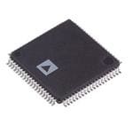
| 描述 | IC QUADRATURE DGTL UPCONV 80LQFP数据转换IC - 各种类型 CMOS 200 MSPS 14-Bit Quadrature |
| DevelopmentKit | AD9857/PCBZ |
| 产品分类 | |
| 品牌 | Analog Devices Inc |
| 产品手册 | |
| 产品图片 |
|
| rohs | 符合RoHS无铅 / 符合限制有害物质指令(RoHS)规范要求 |
| 产品系列 | 数据转换器IC,数据转换IC - 各种类型,Analog Devices AD9857ASTZAD9857 |
| 数据手册 | |
| 产品型号 | AD9857ASTZ |
| RF类型 | HFC 缆线网络 |
| 产品种类 | 数据转换IC - 各种类型 |
| 供应商器件封装 | 80-LQFP(14x14) |
| 分辨率 | 14 bit |
| 功能 | 升频器 |
| 包装 | 托盘 |
| 商标 | Analog Devices |
| 安装风格 | SMD/SMT |
| 封装 | Tray |
| 封装/外壳 | 80-LQFP |
| 封装/箱体 | LQFP-80 |
| 工作温度范围 | - 40 C to + 85 C |
| 工作电源电压 | 3 V to 3.5 V |
| 工厂包装数量 | 90 |
| 标准包装 | 1 |
| 系列 | AD9857 |
| 视频文件 | http://www.digikey.cn/classic/video.aspx?PlayerID=1364138032001&width=640&height=505&videoID=2245193150001 |
| 转换器数量 | 1 |
| 辅助属性 | - |
| 频率 | 5MHz ~ 200MHz |


- 商务部:美国ITC正式对集成电路等产品启动337调查
- 曝三星4nm工艺存在良率问题 高通将骁龙8 Gen1或转产台积电
- 太阳诱电将投资9.5亿元在常州建新厂生产MLCC 预计2023年完工
- 英特尔发布欧洲新工厂建设计划 深化IDM 2.0 战略
- 台积电先进制程称霸业界 有大客户加持明年业绩稳了
- 达到5530亿美元!SIA预计今年全球半导体销售额将创下新高
- 英特尔拟将自动驾驶子公司Mobileye上市 估值或超500亿美元
- 三星加码芯片和SET,合并消费电子和移动部门,撤换高东真等 CEO
- 三星电子宣布重大人事变动 还合并消费电子和移动部门
- 海关总署:前11个月进口集成电路产品价值2.52万亿元 增长14.8%


PDF Datasheet 数据手册内容提取
CMOS 200 MSPS 14-Bit Quadrature Digital Upconverter AD9857 FEATURES 200 MHz internal clock rate 3.3 V single supply 14-bit data path Single-ended or differential input reference clock Excellent dynamic performance: 80-lead LQFP surface-mount packaging 80 dB SFDR @ 65 MHz (±100 kHz) A Three modes of operation: OUT 4× to 20× programmable reference clock multiplier Quadrature modulator mode Reference clock multiplier PLL lock detect indicator Single-tone mode Internal 32-bit quadrature DDS Interpolating DAC mode FSK capability APPLICATIONS 8-bit output amplitude control HFC data, telephony, and video modems Single-pin power-down function Wireless base station Four programmable, pin-selectable signal profiles Agile, LO frequency synthesis SIN(x)/x correction (inverse SINC function) Broadband communications Simplified control interface 10 MHz serial, 2-wire or 3-wire SPI®-compatible FUNCTIONAL BLOCK DIAGRAM INVERSE FIXED AD9857 I CIC FILTER POINLTAETRO-R PROGRAMMABLE QMUOADDURLAATTUORRE DAC_RSET 14 INTERPOLATOR PARD(1AA4LT-BLAIE TILN) DEMUX 14 CINICV MUX (4 ) (2C-I C63 ) MUX UX INVSEINRCSE MUX14 1D4-ABCIT IIOOUUTT M FILTER Q K OL S SIN COS 8 DATA CLOCK INVERSE CIC CLOC NVERSE CIC CONTR HALF-BAND CLOCK INTERP CONTROL INTERP CLOCK TWUONRINDCGDODRS3E2 CLOCK INVERSESINC CLOCK OSVUCATALPULUEET DAC CLOCK I TIMING AND CONTROL CONTROL REGISTERS POWER- PROFILE SYNCH SYSCLK X DOWN SELECT U LOGIC LOGIC M MUCLLTOIPCLKIER MODE REFCLK (4 – 20 ) CONTROL REFCLK PDFCULDK/ TxENABLE RESETOVECRIFCLOW SPEORRIATL PDDOIGOWIWTEANRL- PS1 PS0 LPOLCLK CIMNLOPODUCETK 01018-C-001 Figure 1. Rev. C Information furnished by Analog Devices is believed to be accurate and reliable. However, no responsibility is assumed by Analog Devices for its use, nor for any infringements of patents or other rights of third parties that may result from its use. One Technology Way, P.O. Box 9106, Norwood, MA 02062-9106, U.S.A. Specifications subject to change without notice. No license is granted by implication or otherwise under any patent or patent rights of Analog Devices. Trademarks and Tel: 781.329.4700 www.analog.com registered trademarks are the property of their respective owners. Fax: 781.326.8703 © 2004 Analog Devices, Inc. All rights reserved.
AD9857 TABLE OF CONTENTS Revision History...............................................................................3 Input Data Programming..............................................................24 General Description.........................................................................4 Control Interface—Serial I/O...................................................24 Specifications.....................................................................................5 General Operation of the Serial Interface...............................24 Absolute Maximum Ratings............................................................8 Instruction Byte..........................................................................26 Explanation of Test Levels...........................................................8 Serial Interface Port Pin Descriptions.....................................26 ESD Caution..................................................................................8 Control Register Descriptions..................................................27 Pin Configuration and Function Descriptions.............................9 Profile #0......................................................................................27 Typical Performance Characteristics...........................................11 Profile #1......................................................................................28 Modulated Output Spectral Plots.............................................11 Profile #2......................................................................................28 Single-Tone Output Spectral Plots...........................................12 Profile #3......................................................................................28 Narrow-band SFDR Spectral Plots...........................................13 Latency.........................................................................................30 Output Constellations................................................................14 Ease of Use Features.......................................................................32 Modes Of Operation......................................................................15 Profile Select................................................................................32 Quadrature Modulation Mode.................................................15 Setting the Phase of the DDS....................................................32 Single-Tone Mode......................................................................16 Reference Clock Multiplier.......................................................32 Interpolating DAC Mode..........................................................17 PLL Lock......................................................................................32 Signal Processing Path...................................................................18 Single or Differential Clock......................................................33 Input Data Assembler................................................................18 CIC Overflow Pin.......................................................................33 Inverse CIC Filter.......................................................................19 Clearing the CIC Filter..............................................................33 Programmable (2× to 63×) CIC Interpolating Filter.............21 Digital Power-Down..................................................................33 Quadrature Modulator..............................................................21 Hardware-Controlled Digital Power-Down...........................34 DDS Core.....................................................................................21 Software-Controlled Digital Power-Down.............................34 Inverse SINC Filter.....................................................................22 Full Sleep Mode..........................................................................34 Output Scale Multiplier.............................................................22 Power Management Considerations........................................34 14-Bit D/A Converter................................................................22 Support........................................................................................35 Reference Clock Multiplier.......................................................23 Outline Dimensions.......................................................................38 Ordering Guide..........................................................................39 Rev. C | Page 2 of 40
AD9857 REVISION HISTORY 5/04−Data Sheet Changed from Rev. B to Rev. C 4/02—Changed from Rev. A to Rev. B Changes to 14-Bit D/A Converter Section..................................22 Edit to Functional Block Diagram..................................................1 Changes to Register Address 0Ch, Bit 1 Equation......................28 Edits to Specifications.......................................................................3 Changes to Register Address 12h, Bit 1 Equation.......................28 Edits to Figure 5 ................................................................................6 Changes to Register Address 18h, Bit 1 Equation.......................28 Edits to Figure 18............................................................................11 Added Support Section...................................................................35 Edits to Figure 19............................................................................12 Updated Figure 38...........................................................................38 Edits to Figure 20............................................................................13 Updated Ordering Guide...............................................................39 Edits to Figure 25........................................................................... 16 Edits to Figure 26............................................................................16 Edit to Equation 1...........................................................................16 Edit to Figure 28..............................................................................19 Edit to Notes on Serial Port Operation section...........................21 Edit to Figure 37..............................................................................31 Rev. C| Page 3 of 40
AD9857 GENERAL DESCRIPTION The AD9857 integrates a high speed direct digital synthesizer (DDS), a high performance, high speed, 14-bit digital-to-analog converter (DAC), clock multiplier circuitry, digital filters, and other DSP functions onto a single chip, to form a complete quadrature digital upconverter device. The AD9857 is intended to function as a universal I/Q modulator and agile upconverter, single-tone DDS, or interpolating DAC for communications applications, where cost, size, power dissipation, and dynamic performance are critical attributes. The AD9857 offers enhanced performance over the industry- standard AD9856, as well as providing additional features. The AD9857 is available in a space-saving, surface-mount package and is specified to operate over the extended industrial temperature range of −40°C to +85°C. Rev. C | Page 4 of 40
AD9857 SPECIFICATIONS V = 3.3 V ± 5%, R = 1.96 kΩ, external reference clock frequency = 10 MHz with REFCLK multiplier enabled at 20×. S SET Table 1. Parameter Temp Test Level Min Typ Max Unit REF CLOCK INPUT CHARACTERISTICS Frequency Range REFCLK Multiplier Disabled Full VI 1 200 MHz REFCLK Multiplier Enabled at 4× Full VI 1 50 MHz REFCLK Multiplier Enabled at 20× Full VI 1 10 MHz Input Capacitance 25°C V 3 pF Input Impedance 25°C V 100 MΩ Duty Cycle 25°C V 50 % Duty Cycle with REFCLK Multiplier Enabled 25°C V 35 65 % Differential Input (VDD/2) ±200 mV 25°C V 1.45 1.85 V DAC OUTPUT CHARACTERISTICS Resolution 14 Bits Full-Scale Output Current 5 10 20 mA Gain Error 25°C I 8.5 0 % FS Output Offset 25°C I 2 µA Differential Nonlinearity 25°C V 1.6 LSB Integral Nonlinearity 25°C V 2 LSB Output Capacitance 25°C V 5 pF Residual Phase Noise @ 1 kHz Offset, 40 MHz A OUT REFCLK Multiplier Enabled at 20× 25°C V −107 dBc/Hz REFCLK Multiplier at 4× 25°C V −123 dBc/Hz REFCLK Multiplier Disabled 25°C V −145 dBc/Hz Voltage Compliance Range 25°C I −0.5 +1.0 V Wideband SFDR 1 MHz to 20 MHz Analog Out 25°C V −75 dBc 20 MHz to 40 MHz Analog Out 25°C V −65 dBc 40 MHz to 60 MHz Analog Out 25°C V −62 dBc 60 MHz to 80 MHz Analog Out 25°C V −60 dBc Narrowband SFDR 10 MHz Analog Out (±1 MHz) 25°C V −87 dBc 10 MHz Analog Out (±250 kHz) 25°C V −88 dBc 10 MHz Analog Out (±50 kHz) 25°C V −92 dBc 10 MHz Analog Out (±10 kHz) 25°C V −94 dBc 65 MHz Analog Out (±1 MHz) 25°C V −86 dBc 65 MHz Analog Out (±250 kHz) 25°C V −86 dBc 65 MHz Analog Out (±50 kHz) 25°C V −86 dBc 65 MHz Analog Out (±10 kHz) 25°C V −88 dBc 80 MHz Analog Out (±1 MHz) 25°C V −85 dBc 80 MHz Analog Out (±250 kHz) 25°C V −85 dBc 80 MHz Analog Out (±50 kHz) 25°C V −85 dBc 80 MHz Analog Out (±0 kHz) 25°C V −86 dBc Rev. C| Page 5 of 40
AD9857 Parameter Temp Test Level Min Typ Max Unit MODULATOR CHARACTERISTICS (65 MHz A ) OUT (Input data: 2.5 MS/s, QPSK, 4× oversampled, inverse SINC filter ON, inverse CIC ON) I/Q Offset 25°C IV 55 65 dB Error Vector Magnitude 25°C IV 0.4 1 % INVERSE SINC FILTER (variation in gain from DC to 80 MHz, 25°C V ±0.1 dB inverse SINC filter ON) SPURIOUS POWER (off channel, measured in equivalent bandwidth), Full-Scale Output 6.4 MHz Bandwidth 25°C IV −65 dBc 3.2 MHz Bandwidth 25°C IV −67 dBc 1.6 MHz Bandwidth 25°C IV −69 dBc 0.8 MHz Bandwidth 25°C IV −69 dBc 0.4 MHz Bandwidth 25°C IV −70 dBc 0.2 MHz Bandwidth 25°C IV −72 dBc SPURIOUS POWER (Off channel, measured in equivalent bandwidth), Output Attenuated 18 dB Relative to Full Scale 6.4 MHz Bandwidth 25°C IV −51 dBc 3.2 MHz Bandwidth 25°C IV −54 dBc 1.6 MHz Bandwidth 25°C IV −56 dBc 0.8 MHz Bandwidth 25°C IV −59 dBc 0.4 MHz Bandwidth 25°C IV −62 dBc 0.2 MHz Bandwidth 25°C IV −63 dBc TIMING CHARACTERISTICS Serial Control Bus Maximum Frequency 25°C I 10 MHz Minimum Clock Pulse Width Low (t ) 25°C I 30 ns PWL Minimum Clock Pulse Width High (t ) 25°C I 30 ns PWH Maximum Clock Rise/Fall Time 25°C I 1 ms Minimum Data Setup Time (t ) 25°C I 30 ns DS Minimum Data Hold Time (t ) 25°C I 0 ns DH Maximum Data Valid Time (t ) 25°C I 35 ns DV Wake-Up Time1 25°C I 1 ms Minimum RESET Pulse Width High (t ) 25°C I 5 SYSCLK22Cycles RH Minimum CS Setup Time 25°C I 40 ns CMOS LOGIC INPUTS Logic 1 Voltage 25°C IV 2.0 V Logic 0 Voltage 25°C IV 0.8 V Logic 1 Current 25°C I 5 µA Logic 0 Current 25°C I 5 µA Input Capacitance 25°C V 3 pF CMOS LOGIC OUTPUTS (1 mA LOAD) Logic 1 Voltage 25°C I 2.7 V Logic 0 Voltage 25°C I 0.4 V Rev. C | Page 6 of 40
AD9857 Parameter Temp Test Level Min Typ Max Unit POWER SUPPLY VCURRENT3 (all power specifications at S V = 3.3 V, 25°C, REFCLK = 200 MHz) DD Full Operating Conditions 25°C I 540 615 mA 160 MHz Clock (×16) 25°C I 445 515 mA 120 MHz Clock (×12) 25°C I 345 400 mA Burst Operation (25%) 25°C I 395 450 mA Single-Tone Mode 25°C I 265 310 mA Power-Down Mode 25°C I 71 80 mA Full-Sleep Mode 25°C I 8 13.5 mA 1 Wake-up time refers to recovery from full-sleep mode. The longest time required is for the reference clock multiplier PLL to lock up (if it is being used). The wake-up time assumes that there is no capacitor on DAC_BP, and that the recommended PLL loop filter values are used. The state of the reference clock multiplier lock can be determined by observing the signal on the PLL_LOCK pin. 2 SYSCLK refers to the actual clock frequency used on-chip by the AD9857. If the reference clock multiplier is used to multiply the external reference frequency, the SYSCLK frequency is the external frequency multiplied by the reference clock multiplier multiplication factor. If the reference clock multiplier is not used, the SYSCLK frequency is the same as the external REFCLK frequency. 3 CIC = 2, INV SINC ON, FTW = 40%, PLL OFF, auto power-down between burst On, TxENABLE duty cycle = 25%. Rev. C| Page 7 of 40
AD9857 ABSOLUTE MAXIMUM RATINGS Stresses above those listed under Absolute Maximum Ratings EXPLANATION OF TEST LEVELS may cause permanent damage to the device. This is a stress Table 3. rating only; functional operation of the device at these or any Test Level other conditions above those indicated in the operational 1 100% production tested. section of this specification is not implied. Exposure to absolute 2 100% production tested at 25°C and sample tested at maximum rating conditions for extended periods may affect specific temperatures. device reliability. 3 Sample tested only. 4 Parameter is guaranteed by design and Table 2. characterization testing. Parameter Rating 5 Parameter is a typical value only. Maximum Junction Temperature 150°C 6 Devices are 100% production tested at 25°C and VS 4 V guaranteed by design and characterization testing for Digital Input Voltage −0.7 V to +V industrial operating temperature range. S Digital Output Current 5 mA Storage Temperature −65°C to +150°C Operating Temperature −40°C to +85°C Lead Temperature (Soldering 10 s) 300°C θ 35°C/W JA θ 16°C/W JC ESD CAUTION ESD (electrostatic discharge) sensitive device. Electrostatic charges as high as 4000 V readily accumulate on the human body and test equipment and can discharge without detection. Although this product features proprietary ESD protection circuitry, permanent damage may occur on devices subjected to high energy electrostatic discharges. Therefore, proper ESD precautions are recommended to avoid performance degradation or loss of functionality. Rev. C | Page 8 of 40
AD9857 PIN CONFIGURATION AND FUNCTION DESCRIPTIONS TxENABLE PDCLK/FUD DGND DGND DGND DVDD DVDD DVDD DGND DGND DGND CIC_OVRFL PLL_LOCK RESET DPD AGND AVDD REFCLK REFCLK AGND 80 79 78 77 76 75 74 73 72 71 70 69 68 67 66 65 64 63 62 61 D13 1 60 DIFFCLKEN PIN 1 D12 2 INDICATOR 59 AGND D11 3 58 AVDD D10 4 57 NC D9 5 56 AGND D8 6 55 PLL_FILTER D7 7 54 AVDD DVDD 8 53 AGND DVDD 9 52 NC AD9857 DVDD 10 51 NC TOP VIEW DGND 11 (Not to Scale) 50 DAC_RSET DGND 12 49 DAC_BP DGND 13 48 AVDD D6 14 47 AGND D5 15 46 IOUT D4 16 45 IOUT D3 17 44 AGND D2 18 43 AVDD D1 19 42 AGND D0 20 41 NC 21 22 23 24 25 26 27 28 29 30 31 32 33 34 35 36 37 38 39 40 NC = NO CONNECT PS1 PS0 CS SCLK SDIO SDO SYNCIO DGND DGND DGND DVDD DVDD DVDD NC AVDD AGND AVDD AVDD AGND AGND 01018-C-000 Figure 2. Pin Configuration Table 4. Pin Function Descriptions Pin Number Mnemonic I/O Function 20–14, 7–1 D0–D6, D7– I 14-Bit Parallel Data Bus for I and Q Data. The required numeric format is twos complement with D13 D13 as the sign bit and D12–D0 as the magnitude bits. Alternating 14-bit words are demultiplexed onto the I and Q data pathways (except when operating in the interpolating DAC mode, in which case every word is routed onto the I data path). When the TxENABLE pin is asserted high, the next accepted word is presumed to be I data, the next Q data, and so forth. 8–10, 31–33, DVDD 3.3 V Digital Power pin(s). 73–75 11–13, 28–30, DGND Digital Ground pin(s). 70–72, 76–78 21 PS1 I Profile Select Pin 1. The LSB of the two profile select pins. In conjunction with PS0, selects one of four profile configurations. 22 PS0 I Profile Select Pin 0. The MSB of the two profile select pins. In conjunction with P1, selects one of four profile configurations. 23 CS I Serial Port Chip Select pin. An active low signal that allows multiple devices to operate on a single serial bus. 24 SCLK I Serial Port Data Clock pin. The serial data CLOCK for the serial port. 25 SDIO I/O Serial Port Input/Output Data pin. Bidirectional serial DATA pin for the serial port. This pin can be programmed to operate as a serial input only pin, via the control register bit 00h<7>. The default state is bidirectional. 26 SDO O Serial Port Output Data pin. This pin serves as the serial data output pin when the SDIO pin is configured for serial input only mode. The default state is three-state. 27 SYNCIO I Serial Port Synchronization pin. Synchronizes the serial port without affecting the programmable register contents. This is an active high input that aborts the current serial communication cycle. 34, 41, 51, 52, NC No connect. 57 Rev. C| Page 9 of 40
AD9857 Pin Number Mnemonic I/O Function 35, 37, 38, 43, AVDD 3.3 V Analog Power pin(s). 48, 54, 58, 64 36, 39, 40, 42, AGND Analog Ground pin(s). 44, 47, 53, 56, 59, 61, 65 45 IOUT O DAC Output pin. Normal DAC output current (analog). 46 IOUT O DAC Complementary Output pin. Complementary DAC output current (analog). 49 DAC_BP DAC Reference Bypass. Typically not used. 50 DAC_RSET I DAC Current Set pin. Sets DAC reference current. 55 PLL_FILTER O PLL Filter. R-C network for PLL filter. 60 DIFFCLKEN I Clock Mode Select pin. A logic high on this pin selects DIFFERENTIAL REFCLK input mode. A logic low selects the SINGLE-ENDED REFCLK input mode. 62 REFCLK I Reference Clock pin. In single-ended clock mode, this pin is the Reference Clock input. In differential clock mode, this pin is the positive clock input. 63 REFCLK I Inverted Reference Clock pin. In differential clock mode, this pin is the negative clock input. 66 DPD I Digital Power-Down pin. Assertion of this pin shuts down the digital sections of the device to conserve power. However, if selected, the PLL remains operational. 67 RESET I Hardware RESET pin. An active high input that forces the device into a predefined state. 68 PLL_LOCK O PLL Lock pin. Active high output signifying, in real time, when PLL is in lock state. 69 CIC_OVRFL O CIC Overflow pin. Activity on this pin indicates that the CIC Filters are in “overflow” state. This pin is typically low unless a CIC overflow occurs. 79 PDCLK/FUD I/O Parallel Data Clock/Frequency Update pin. When not in single-tone mode, this pin is an output signal that should be used as a clock to synchronize the acceptance of the 14-bit parallel data-words on Pins D13–D0. In single-tone mode, this pin is an input signal that synchronizes the transfer of a changed frequency tuning word (FTW) in the active profile (PSx) to the accumulator (FUD = frequency update signal). When profiles are changed by means of the PS–PS1 pins, the FUD does not have to be asserted to make the FTW active. 80 TxENABLE I When TxENABLE is asserted, the device processes the data through the I and Q data pathways; otherwise 0s are internally substituted for the I and Q data entering the signal path. The first data word accepted when the TxENABLE is asserted high is treated as I data, the next data word is Q data, and so forth. Rev. C | Page 10 of 40
AD9857 TYPICAL PERFORMANCE CHARACTERISTICS MODULATED OUTPUT SPECTRAL PLOTS 0 0 –10 –10 –20 –20 –30 –30 –40 –40 B –50 B –50 d d –60 –60 –70 –70 –80 –80 –1–0900START 0Hz 5MHz/ STOP 50MHz 01018-C-003 –1–9000START 0Hz 8MHz/ STOP 80MHz 01018-C-005 Figure 3. QPSK at 42 MHz and 2.56 MS/s; 10.24 MHz External Clock Figure 5. 16-QAM at 65 MHz and 1.28 MS/s; 10.24 MHz External Clock with REFCLK Multiplier = 12, CIC Interpolation Rate = 3, with REFCLK Multiplier = 18, CIC Interpolation Rate = 9, 4× Oversampled Data 4× Oversampled Data 0 0 –8 –8 –16 –16 –24 –24 –32 –32 B –40 B –40 d d –48 –48 –56 –56 –64 –64 ––7820START 0Hz 4MHz/ STOP 40MHz 01018-C-004 ––7820SSTTAARRTT 00HHzz 5MHz/ STOP 50MHz 01018-C-006 Figure 4. 64-QAM at 28 MHz and 6 MS/s; 36 MHz External Clock Figure 6. 256-QAM at 38 MHz and 6 MS/s; 48 MHz External Clock with REFCLK Multiplier = 4, CIC Interpolation Rate = 2, with REFCLK Multiplier = 4, CIC Interpolation Rate = 2, 3× Oversampled Data 4× Oversampled Data Rev. C| Page 11 of 40
AD9857 SINGLE-TONE OUTPUT SPECTRAL PLOTS 0 0 –10 –10 –20 –20 –30 –30 –40 –40 B–50 B –50 d d –60 –60 –70 –70 –80 –80 –1–9000 START 0Hz 10MHz/ STOP 100MHz 01018-C-007 –1–0900START 0Hz 10MHz/ STOP 100MHz 01018-C-009 Figure 7. 21 MHz Single-Tone Output Figure 9. 42 MHz Single-Tone Output 0 0 –10 –10 –20 –20 –30 –30 –40 –40 B –50 B –50 d d –60 –60 –70 –70 –80 –80 –1–0900START 0Hz 10MHz/ STOP 100MHz 01018-C-008 –1–9000START 0Hz 10MHz/ STOP 100MHz 01018-C-010 Figure 8. 65 MHz Single-Tone Output Figure 10. 79 MHz Single-Tone Output Rev. C | Page 12 of 40
AD9857 NARROW-BAND SFDR SPECTRAL PLOTS 0 0 –10 –10 –20 –20 –30 –30 –40 –40 B –50 B –50 d d –60 –60 –70 –70 –80 –80 –1–0900 CENTER 70.1MHz 10kHz/ SPAN 100kHz 01018-C-011 –1–0900CENTER 70.1MHz 10kHz/ SPAN 100kHz 01018-C-012 Figure 11. 70.1 MHz Narrow-Band SFDR, 10 MHz External Clock Figure 12. 70.1 MHz Narrow-Band SFDR, 200 MHz External Clock with REFCLK Multiplier = 20 with REFCLK Multiplier Disabled Rev. C| Page 13 of 40
AD9857 OUTPUT CONSTELLATIONS 1 1 CONST CONST 200m/DIV 200m/DIV –1–1.3071895838 1.30718958378 01018-C-013 –1–1.3071895838 1.30718958378 01018-C-016 Figure 13. QPSK, 65 MHz, 2.56 MS/s Figure 16. 16-QAM, 65 MHz, 2.56 MS/s 1 1 CONST CONST 200m/DIV 200m/DIV –1–1.3071895838 1.30718958378 01018-C-014 –1–1.3071895838 1.30718958378 01018-C-017 Figure 14. 64-QAM, 42 MHz, 6 MS/s Figure 17. 256-QAM, 42 MHz, 6 MS/s 1 CONST 200m/DIV –1–1.3071895838 1.30718958378 01018-C-015 Figure 15. GMSK Modulation, 13 MS/s Rev. C | Page 14 of 40
AD9857 MODES OF OPERATION of PDCLK. The PDCLK operates at twice the rate of either the I The AD9857 has three operating modes: or Q data path. This is due to the fact that the I and Q data must • Quadrature modulation mode (default) be presented to the parallel port as two 14-bit words • Single-tone mode multiplexed in time. One I word and one Q word together • Interpolating DAC mode comprise one internal sample. Each sample is propagated along Mode selection is accomplished by programming a control the internal data pathway in parallel fashion. register via the serial port. The inverse SINC filter and output The DDS core provides a quadrature (sin and cos) local scale multiplier are available in all three modes. oscillator signal to the quadrature modulator, where the I and Q QUADRATURE MODULATION MODE data are multiplied by the respective phase of the carrier and summed together, to produce a quadrature-modulated data In quadrature modulation mode, both the I and Q data paths stream. are active. A block diagram of the AD9857 operating in the quadrature modulation mode is shown in Figure 18. All of this occurs in the digital domain, and only then is the digital data stream applied to the 14-bit DAC to become the In quadrature modulation mode, the PDCLK/FUD pin is an quadrature-modulated analog output signal. output and functions as the parallel data clock (PDCLK), which serves to synchronize the input of data to the AD9857. In this mode, the input data must be synchronized with the rising edge INVERSE FIXED AD9857 I CIC FILTER POINLTAETRO-R PROGRAMMABLE QMUOADDURLAATTUORRE DAC_RSET 14 INTERPOLATOR PARD(1AA4LT-BLAIE TILN) DEMUX 14 CINICV MUX (4 ) (2C-I C63 ) MUX UX INVSEINRCSE MUX14 1D4-ABCIT IIOOUUTT M FILTER Q K OL S SIN COS 8 DATA CLOCK INVERSE CIC CLOC NVERSE CIC CONTR HALF-BAND CLOCK INTERP CONTROL INTERP CLOCK TWUONRINDCGDODRS3E2 CLOCK INVERSESINC CLOCK OSVUCATALPULUEET DAC CLOCK I TIMING AND CONTROL CONTROL REGISTERS POWER- PROFILE SYNCH SYSCLK X DOWN SELECT U LOGIC LOGIC M MUCLLTOIPCLKIER MODE REFCLK (4 – 20 ) CONTROL REFCLK PDFCULDK/ TxENABLE RESETOVECRIFCLOW SPEORRIATL PDDOIGOWIWTEANRL- PS1 PS0 LPOLCLK CIMNLOPODUCETK 01018-C-018 Figure 18. Quadrature Modulation Mode Rev. C| Page 15 of 40
AD9857 SINGLE-TONE MODE A block diagram of the AD9857 operating in the single-tone In the single-tone mode, no 14-bit parallel data is applied to the mode is shown in Figure 19. In the single-tone mode, both the AD9857. The internal DDS core is used to produce a single I and Q data paths are disabled from the 14-bit parallel data frequency signal according to the tuning word. The single-tone port up to and including the modulator. The PDCLK/ FUD pin signal then moves toward the output, where the inverse SINC is an input and functions as a frequency update (FUD) control filter and the output scaling can be applied. Finally, the digital signal. This is necessary because the frequency tuning word is single-tone signal is converted to the analog domain by the programmed via the asynchronous serial port. The FUD signal 14-bit DAC. causes the new frequency tuning word to become active. In single-tone mode, the cosine portion of the DDS serves as the signal source. The output signal consists of a single frequency as determined by the tuning word stored in the appropriate control register, per each profile. AD9857 DAC_RSET UX14 14-BIT IOUT INVERSE M DAC IOUT SINC FILTER S 8 O C K DDS SEOCK OSUCTAPLUET CLOC TUNINCGORE LOCK INVERSINC CL VALUE DAC WORD 32 C TIMING AND CONTROL CONTROL REGISTERS POWER- PROFILE SYNCH SYSCLK X DOWN SELECT U LOGIC LOGIC M MUCLLTOIPCLKIER MODE REFCLK (4 – 20 ) CONTROL REFCLK PDFCULDK/ RESET SPEORRIATL PDDOIGOWIWTEANRL- PS1 PS0 LPOLCLK CIMNLOPODUCETK 01018-C-001 Figure 19. Single-Tone Mode Rev. C | Page 16 of 40
AD9857 INTERPOLATING DAC MODE A block diagram of the AD9857 operating in the interpolating In the Interpolating DAC mode, the baseband data supplied at DAC mode is shown in Figure 20. In this mode, the DDS and the parallel port remains at baseband at the output; that is, no modulator are both disabled and only the I data path is active. modulation takes place. However, a sample rate conversion The Q data path is disabled from the 14-bit parallel data port up takes place based on the programmed interpolation rate. The to and including the modulator. interpolation hardware performs the necessary signal processing required to eliminate the aliased images at baseband As in the quadrature modulation mode, the PDCLK pin is an that would otherwise result from a sample rate conversion. The output and functions as a clock which serves to synchronize the interpolating DAC function is effectively an oversampling input of data to the AD9857. Unlike the quadrature modulation operation with the original input spectrum intact but sampled mode, however, the PDCLK operates at the rate of the I data at a higher rate. path. This is because only I data is being presented to the parallel port as opposed to the interleaved I/Q format of the quadrature modulation mode. INVERSE FIXED AD9857 I CIC FILTER POINLTAETRO-R PROGRAMMABLE DAC_RSET INTERPOLATOR PARD(1AA4LT-BLAIE TILN) DEMUX 14 CINICV MUX (4 ) (2C-I C63 ) MUX INVSEINRCSE MUX 14 1D4-ABCIT IIOOUUTT FILTER 8 L K O S DATA CLOCK INVERSE CIC CLOC NVERSE CIC CONTR HALF-BAND CLOCK INTERP CONTROL INTERP CLOCK INVERSESINC CLOCK OSVUCATALPULUEET DAC CLOCK I TIMING AND CONTROL CONTROL REGISTERS POWER- PROFILE SYNCH SYSCLK X DOWN SELECT U LOGIC LOGIC M MUCLLTOIPCLKIER MODE REFCLK (4 – 20 ) CONTROL REFCLK PDFCULDK/ TxENABLE RESETOVECRIFCLOW SPEORRIATL PDDOIGOWIWTEANRL- PS1 PS0 LPOLCLK CIMNLOPODUCETK 01018-C-001 Figure 20. Interpolating DAC Mode Rev. C| Page 17 of 40
AD9857 SIGNAL PROCESSING PATH to the accumulator of the DDS, thus starting the frequency To better understand the operation of the AD9857 it is helpful synthesis process. to follow the signal path from input, through the device, to the output, examining the function of each block (refer to Figure 1). After loading the frequency tuning word to a profile, a FUD The input to the AD9857 is a 14-bit parallel data path. This signal is not needed when switching between profiles using the assumes that the user is supplying the data as interleaved I and two profile select pins (PS0, PS1). When switching between Q values. Any encoding, interpolation, and pulse shaping of the profiles, the frequency tuning word in the profile register data stream should occur before the data is presented to the becomes effective. AD9857 for upsampling. In the quadrature modulation mode, the PDCLK rate is twice The AD9857 demultiplexes the interleaved I and Q data into the rate of the I (or Q) data rate. The AD9857 expects two separate data paths inside the part. This means that the interleaved I and Q data words at the parallel port with one input sample rate (f ), the rate at which 14-bit words are DATA word per PDCLK rising edge. One I word and one Q word presented to the AD9857, must be 2× the internal I/Q Sample together comprise one internal sample. Each sample is Rate (f ), the rate at which the I/Q pairs are processed. In other IQ propagated along the internal data pathway in parallel. words, f = 2 × f . DATA IQ In the interpolating DAC mode, however, the PDCLK rate is the From the input demultiplexer to the quadrature modulator, the same as the I data rate because the Q data path is inactive. In data path of the AD9857 is a dual I/Q path. this mode, each PDCLK rising edge latches a data word into the I data path. All timing within the AD9857 is provided by the internal system clock (SYSCLK) signal. The externally provided The PDCLK is provided as a continuous clock (i.e., always reference clock signal may be used as is (1×), or multiplied by active). However, the assertion of PDCLK may be optionally the internal clock multiplier (4×−20×) to generate the SYSCLK. qualified internally by the PLL lock indicator if the user elects All other internal clocks and timing are derived from the to set the PLL lock control bit in the appropriate control register. SYSCLK. Data supplied by the user to the 14-bit parallel port is latched INPUT DATA ASSEMBLER into the device coincident with the rising edge of the PDCLK. In the quadrature modulation or interpolating DAC modes, the In the quadrature modulation mode, the rising edge of the device accepts 14-bit, twos complement data at its parallel data TxENABLE signal is used to synchronize the device. While port. The timing of the data supplied to the parallel port may be TxENABLE is in the Logic 0 state, the device ignores the 14-bit easily facilitated with the PDCLK/FUD pin of the AD9857, data applied to the parallel port and allows the internal data which is an output in the quadrature modulation mode and the path to be flushed by forcing 0s down the I and Q data pathway. interpolating DAC mode. In the single-tone mode, the same pin On the rising edge of TxENABLE, the device is ready for the becomes an input to the device and serves as a frequency first I word. The first I word is latched into the device update (FUD) strobe. coincident with the rising edge of PDCLK. The next rising edge of PDCLK latches in a Q word, etc., until TxENABLE is set to a Frequency control words are programmed into the AD9857 via Logic 0 state by the user. the serial port (see the Control Register description). Because the serial port is an asynchronous interface, when programming When in the quadrature modulation mode, it is important that new frequency tuning words into the on-chip profile registers, the user ensure that an even number of PDCLK intervals are the AD9857’s internal frequency synthesizer must be observed during any given TxENABLE period. This is because synchronized with external events. The purpose of the FUD the device must capture both an I and a Q value before the data input pin is to synchronize the start of the frequency can be processed along the internal data pathway. synthesizer to the external timing requirements of the user. The The timing relationship between TxENABLE, PDCLK, and rising edge of the FUD signal causes the frequency tuning word DATA is shown in Figure 21 and Figure 22. of the selected profile (see the Profile section) to be transferred Rev. C | Page 18 of 40
AD9857 TxENABLE tDS tDH PDCLK t DS D<13:0> I0tDH Q0 I1 Q1 IN QN 01018-C-021 Figure 21. 14-Bit Parallel Port Timing Diagram—Quadrature Modulation Mode TxENABLE tDS tDH PDCLK t DS D<13:0> I0tDH I1 I2 I3 IK– 1 IK 01018-C-022 Figure 22. 14-Bit Parallel Port Timing Diagram—Interpolating DAC Mode Table 5. Parallel Data Bus Timing If the CIC filter is employed, the inband attenuation gradient Symbol Definition Minimum could pose a problem for those applications requiring an tDS Data Setup Time 4 ns extremely flat pass band. For example, if the spectrum of the tDH Data Hold Time 0 ns data as supplied to the AD9857 I or Q path occupies a significant portion of the one-half f region, the higher DATA INVERSE CIC FILTER frequencies of the data spectrum receives slightly more attenuation than the lower frequencies (the worst-case overall The inverse cascaded integrator comb (CIC) filter precompen- droop from f = 0 to one-half f is < 0.8 dB). This may not be DATA sates the data to offset the slight attenuation gradient imposed acceptable in certain applications. The inverse CIC filter has a by the CIC filter. See the Programmable (2× to 63×) CIC response characteristic that is the inverse of the CIC filter Interpolating Filter section. The I (or Q) data entering the first response over the one-half f region. DATA half-band filter occupies a maximum bandwidth of one-half f as defined by Nyquist (where f is the sample rate at the The net result is that the product of the two responses yields in DATA DATA input of the first half-band filter). This is shown graphically in an extremely flat pass band, thereby eliminating the inband Figure 23. attenuation gradient introduced by the CIC filter. The price to be paid is a slight attenuation of the input signal of approx- INBAND imately 0.5 dB for a CIC interpolation rate of 2 and 0.8 dB for ATTENUATION GRADIENT interpolation rates of 3 to 63. The inverse CIC filter is implemented as a digital FIR filter with a response characteristic that is the inverse of the CIC FILTER RESPONSE programmable CIC interpolator. The product of the two responses yields a nearly flat response over the baseband Nyquist bandwidth. The inverse CIC filter provides frequency compensation that yields a response flatness of ±0.05 dB over the baseband Nyquist bandwidth, allowing the AD9857 to provide excellent SNR over its performance range. fDATA/2fDATA 4fDATAf 01018-C-023 TRhegei sintevre r0s6eh C<0IC> . fIitl tiesr a cuatno mbea tbiycaplalyss beydp bays sseedtt iifn tgh Ce oCnItCro l Figure 23. CIC Filter Response interpolation rate is 1×. Whenever this stage is bypassed, power to the stage is shutoff, thereby reducing power dissipation. Rev. C| Page 19 of 40
AD9857 Fixed Interpolator (4×) 0.010 This block is a fixed 4× interpolator. It is implemented as two 0.008 half-band filters. The output of this stage is the original data 0.006 upsampled by 4×. 0.004 Before presenting a detailed description of the half-band filters, B) 0.002 d recall that in the case of the quadrature modulation mode the N ( 0 AI input data stream is representative of complex data; i.e., two G–0.002 input samples are required to produce one I/Q data pair. The –0.004 I/Q sample rate is one-half the input data rate. The I/Q sample –0.006 rate (the rate at which I or Q samples are presented to the input –0.008 of the first half-band filter) is referred to as f . Because the IQ AofD th9e8 5in7t iesr an aqlu Ia/dQr astaumrep lme opdaiurlsa. tIot rs, hfIoQu rledp brees eemntps hthaesi zbeadse hbearned –0.0100 RELATIV0E.0 F5REQUEN0C.1Y0 (HB1 OUT0.P1U5T SAMPL0E.2 R0ATE = 1)0.25 01018-C-025 that f is not the same as the baseband of the user’s symbol rate IQ Figure 25. Combined Half-Band 1 and 2 Pass Band Detail; data, which must be upsampled before presentation to the Frequency Relative to HB1 Output Sample Rate AD9857 (as explained later). The I/Q sample rate (f ) puts a IQ The usable bandwidth of the filter chain puts a limit on the limit on the minimum bandwidth necessary to transmit the f IQ maximum data rate that can be propagated through the spectrum. This is the familiar Nyquist limit and is equal to one- AD9857. A look at the pass band detail of the half-band filter half f , hereafter referred to as f . IQ NYQ response (Figure 25) indicates that in order to maintain an amplitude error of no more than 1 dB, signals are restricted to Together, the two half-band filters provide a factor-of-four having a bandwidth of no more than about 90% of f . Thus, to increase in the sampling rate (4 × f or 8 × f ). Their NYQ IQ NYQ keep the bandwidth of the data in the flat portion of the filter combined insertion loss is 0.01 dB, so virtually no loss of signal pass band, the user must oversample the baseband data by at level occurs through the two half-band filters. Both half-band least a factor of two prior to presenting it to the AD9857. Note filters are linear phase filters, so that virtually no phase that without oversampling, the Nyquist bandwidth of the distortion is introduced within the pass band of the filters. This baseband data corresponds to the f . Because of this, the is an important feature as phase distortion is generally NYQ upper end of the data bandwidth suffers 6 dB or more of intolerable in a data transmission system. attenuation due to the frequency response of the half-band The half-band filters are designed so that their composite filters. Furthermore, if the baseband data applied to the AD9857 performance yields a usable pass band of 80% of the baseband has been pulse shaped, there is an additional concern. Nyquist frequency (0.2 on the frequency scale below). Within Typically, pulse shaping is applied to the baseband data via a that pass band, the ripple does not exceed 0.002 dB. The stop filter having a raised cosine response. In such cases, an α value is band extends from 120% to 400% of the baseband Nyquist used to modify the bandwidth of the data where the value of α frequency (0.3 to 1.0 on the frequency scale) and offers a is such that ≤ α ≤ 1. A value of 0 causes the data bandwidth to minimum of 85 dB attenuation. Figure 24 and Figure 25 show correspond to the Nyquist bandwidth. A value of 1 causes the the composite response of the two half-band filters together. data bandwidth to be extended to twice the Nyquist bandwidth. 10 Thus, with 2× oversampling of the baseband data and α = 1, the 0 Nyquist bandwidth of the data corresponds with the I/Q –10 0.2 0.3 Nyquist bandwidth. As stated earlier, this results in problems –20 near the upper edge of the data bandwidth due to the roll-off –30 –40 attenuation of the half-band filters. Figure 26 illustrates the E AT –50 relationship between α and the bandwidth of raised cosine E R –60 shaped pulses. The problem area is indicated by the shading in PL –70 AM –80 –85 the tail of the pulse with α = 1 which extends into the roll-off S –90 region of the half-band filter. –100 The effect of raised cosine filtering on baseband pulse –110 –120 bandwidth, and the relationship to the half-band filter response –130 are shown in Figure 26. –1400 0.2 0.4 0.6 0.F8REQ1U.0ENC1Y.2 1.4 1.6 1.8 2.0 01018-C-024 Figure 24. Half-Band 1 and 2 Frequency Response; Frequency Relative to HB1 Output Sample Rate Rev. C | Page 20 of 40
AD9857 A) The transfer function of the CIC interpolating filter is 5 ⎛R−1 ⎞ BANDWIDTH H(f)=⎜ ∑e−j(2πfk)⎟ (1) OF I OR Q ⎝k=0 ⎠ DATA 1 SAMPLE RATE where R is the interpolation rate, and f is the frequency relative to SYSCLK. f fNYQ(@1 ) fIQ QUADRATURE MODULATOR B) = 0 The digital quadrature modulator stage is used to frequency shift the baseband spectrum of the incoming data stream up to = 0.5 = 1 fIQ: DATA VECTOR RATE the desired carrier frequency (this process is known as AT INPUT TO AD9857 upconversion). 2× OVERSAMPLE RATE At this point the incoming data has been converted from an incoming sampling rate of f to an I/Q sampling rate equal to f IN fNYQ(@1 ) fNYQ(@2 ) fIQ SYSCLK. The purpose of the upsampling process is to make the data sampling rate equal to the sampling rate of the carrier C) signal. HALF-BAND FILTER RESPONSE The carrier frequency is controlled numerically by a Direct Digital Synthesizer (DDS). The DDS uses the internal reference clock (SYSCLK) to generate the desired carrier frequency with a 2 OVERSAMPLE RATE high degree of precision. The carrier is applied to the I and Q fNYQ(@1 ) fNYQ(@2 ) fIQ f 01018-C-026 msuumltmipelide rtso iyni eqluda ad draattuar set rfeaashmio tnh a(t9 0re°p prhesaesne tosf tfhseet )q uanaddr ature modulated carrier. Figure 26. Effect of Alpha The modulation is done digitally which eliminates the phase and gain imbalance and crosstalk issues typically associated PROGRAMMABLE (2× TO 63×) CIC with analog modulators. Note that the modulated “signal” is INTERPOLATING FILTER actually a number stream sampled at the rate of SYSCLK, the The programmable interpolator is implemented as a CIC filter. same rate at which the output D/A converter is clocked. It is programmable by a 6-bit control word, giving a range of The quadrature modulator operation is also controlled by 2× to 63× interpolation. This interpolator has a low-pass spectral invert bits in each of the four profiles. The quadrature frequency characteristic that is compensated by the inverse CIC modulation takes the form: filter. I×cos(ω)+Q×sin(ω) The programmable interpolator can be bypassed to yield a 1× (no interpolation) configuration by setting the bit in the when the spectral invert bit is set to a Logic 1. appropriate control register, per each profile. Whenever the programmable interpolator is bypassed (1× CIC rate), power to I×cos(ω)−Q×sin(ω) the stage is removed. If the programmable interpolator is bypassed, the inverse CIC filter (see above) is automatically when the spectral invert bit is set to a Logic 0. bypassed, because its compensation is not needed in this case. DDS CORE The output of the programmable interpolator is the data from The direct digital synthesizer (DDS) block generates the sin/cos the 4× interpolator upsampled by an additional 2× to 63×, carrier reference signals that digitally modulate the I/Q data according to the rate chosen by the user. This results in the paths. The DDS frequency is tuned via the serial control port input data being upsampled by a factor of 8× to 252×. with a 32-bit tuning word (per profile). This allows the AD9857’s output carrier frequency to be very precisely tuned while still providing output frequency agility. Rev. C| Page 21 of 40
AD9857 Because the AD9857 defaults to the Modulation mode, the The equation relating output frequency (f ) of the AD9857 OUT default value for the multiplier is B5h (which corresponds digital modulator to the frequency tuning word (FTWORD) to √2). and the system clock (SYSCLK) is f =(FTWORD×SYSCLK)/232 (2) Programming the output scale multiplier to unity gain (80h) OUT bypasses the stage, reducing power dissipation. where f and SYSCLK frequencies are in Hz and FTWORD is OUT 14-BIT D/A CONVERTER a decimal number from 0 to 2,147,483,647 (231−1). A 14-bit digital-to-analog converter (DAC) is used to convert For example, find the FTWORD for fOUT = 41 MHz and the digitally processed waveform into an analog signal. The SYSCLK = 122.88 MHz worst-case spurious signals due to the DAC are the harmonics of the fundamental signal and their aliases (please see the If f = 41 MHz and SYSCLK = 122.88 MHz, then OUT Analog Devices DDS Technical Tutorial, accessible from the FTWORD=556AAAAB hex (3) DDS Technical Library at www.analog.com/dds for a detailed explanation of aliases). The wideband 14-bit DAC in the Loading 556AAAABh into Control Bus Registers 08h–0Bh AD9857 maintains spurious-free dynamic range (SFDR) (for Profile 1) programs the AD9857 for fOUT = 41 MHz, given a performance of −60 dBc up to AOUT = 42 MHz and −55 dBc up SYSCLK frequency of 122.88 MHz. to AOUT = 65 MHz. INVERSE SINC FILTER The conversion process produces aliased components of the fundamental signal at n × SYSCLK ± FCARRIER (n = 1, 2, 3). The sampled carrier data stream is the input to the digital-to- These are typically filtered with an external RLC filter at the analog converter (DAC) integrated onto the AD9857. The DAC output. It is important for this analog filter to have a DAC output spectrum is shaped by the characteristic sin(x)/x sufficiently flat gain and linear phase response across the (or SINC) envelope, due to the intrinsic zero-order hold effect bandwidth of interest to avoid modulation impairments. associated with DAC-generated signals. Because the shape of the SINC envelope is well known, it can be compensated for. The AD9857 provides true and complemented current outputs This envelope restoration function is provided by the optional on A and A , respectively. The full-scale output current is OUT OUT inverse SINC filter preceding the DAC. This function is set by the RSET resistor at DAC_RSET. The value of RSET for a implemented as an FIR filter, which has a transfer function that particular IOUT is determined using the following equation: is the exact inverse of the SINC response. When the inverse SINC filter is selected, it modifies the incoming data stream so RSET =39.93/IOUT (4) that the desired carrier envelope, which would otherwise be shaped by the SINC envelope, is restored. However, this For example, if a full-scale output current of 20 mA is desired, correction is only complete for carrier frequencies up to then RSET = (39.93/0.02), or approximately 2 kΩ. Every approximately 45% of SYSCLK. doubling of the RSET value halves the output current. Note also that the inverse SINC filter introduces about a 3.5 dB The full-scale output current range of the AD9857 is 5 mA−20 loss at low frequencies as compared to the gain with the inverse mA. Full-scale output currents outside of this range degrade SINC filter turned off. This is done to flatten the overall gain SFDR performance. SFDR is also slightly affected by output from dc to 45% of SYSCLK. matching; the two outputs should be terminated equally for best SFDR performance. The inverse SINC filter can be bypassed if it is not needed. If the inverse SINC filter is bypassed, its clock is stopped, thus The output load should be located as close as possible to the reducing the power dissipation of the part. AD9857 package to minimize stray capacitance and inductance. The load may be a simple resistor to ground, an op amp OUTPUT SCALE MULTIPLIER current-to- voltage converter, or a transformer-coupled circuit. An 8-bit multiplier (output scale value in the block diagram) Driving an LC filter without a transformer requires that the preceding the DAC provides the user with a means of adjusting filter be doubly terminated for best performance. Therefore, the the final output level. The multiplier value is programmed via filter input and output should both be resistively terminated the appropriate control registers, per each profile. The LSB with the appropriate values. The parallel combination of the weight is 2–7, which yields a multiplier range of 0 to 1.9921875, two terminations determines the load that the AD9857 sees or nearly 2×. Because the quadrature modulator has an intrinsic for signals within the filter pass band. For example, a loss of 3 dB (1/√2), programming the multiplier for a value of 50 Ω terminated input/ output low-pass filter looks like a √2) restores the data to the full-scale range of the DAC when 25 Ω load to the AD9857. the device is operating in the quadrature modulation mode. Rev. C | Page 22 of 40
AD9857 hum or clock feed-through that is equally present on both input The output compliance voltage of the AD9857 is −0.5 V to signals. The AD9857 true and complement outputs can be +1.0 V. Any signal developed at the DAC output should not differentially combined using a broadband 1:1 transformer with exceed 1.0 V, otherwise, signal distortion results. Furthermore, a grounded, center-tapped primary to perform differential the signal may extend below ground as much as 0.5 V without combining of the two DAC outputs. damage or signal distortion. The use of a transformer with a grounded center tap for common-mode rejection results in REFERENCE CLOCK MULTIPLIER signals at the AD9857 DAC output pins that are symmetrical It is often difficult to provide a high quality oscillator with an about ground. output in the frequency range of 100 MHz – 200 MHz. The As previously mentioned, by differentially combining the two AD9857 allows the use of a lower-frequency oscillator that can signals, the user can provide some degree of common-mode be multiplied to a higher frequency by the on-board reference signal rejection. A differential combiner might consist of a clock multiplier, implemented with a phase locked loop transformer or an op amp. The object is to combine or amplify architecture. See the Ease of Use Features section for a more only the difference between two signals and to reject any thorough discussion of the reference clock multiplier feature. common, usually undesirable, characteristic, such as 60 Hz Rev. C| Page 23 of 40
AD9857 INPUT DATA PROGRAMMING CONTROL INTERFACE—SERIAL I/O the data transfer (1-4), and the starting register address for the first byte of the data transfer. The AD9857 serial port is a flexible, synchronous, serial communications port allowing easy interface to many industry- The first eight SCLK rising edges of each communication cycle standard microcontrollers and microprocessors. The serial I/O are used to write the instruction byte into the AD9857. The is compatible with most synchronous transfer formats, remaining SCLK edges are for Phase 2 of the communication including both the Motorola 6905/11 SPI and Intel 8051 SSR cycle. Phase 2 is the actual data transfer between the AD9857 protocols. and the system controller. Phase 2 of the communication cycle is a transfer of 1, 2, 3, or 4 data bytes as determined by the The interface allows read/write access to all registers that instruction byte. Typically, using one communication cycle in a configure the AD9857. Single or multiple byte transfers are multibyte transfer is the preferred method. However, single-byte supported as well as MSB first or LSB first transfer formats. The communication cycles are useful to reduce CPU overhead when AD9857’s serial interface port can be configured as a single pin register access requires one byte only. An example of this may I/O (SDIO) or two unidirectional pins for in/out (SDIO/SDO). be to write the AD9857 SLEEP bit. GENERAL OPERATION OF THE SERIAL INTERFACE At the completion of any communication cycle, the AD9857 There are two phases to a communication cycle with the serial port controller expects the next eight rising SCLK edges AD9857. Phase 1 is the instruction cycle, which is the writing of to be the instruction byte of the next communication cycle. an instruction byte into the AD9857, coincident with the first All data input to the AD9857 is registered on the rising edge of eight SCLK rising edges. The instruction byte provides the SCLK. All data is driven out of the AD9857 on the falling edge AD9857 serial port controller with information regarding the of SCLK. data transfer cycle, which is Phase 2 of the communication cycle. The Phase 1 instruction byte defines whether the Figure 27 and Figure 28 illustrate the data write and data read upcoming data transfer is read or write, the number of bytes in operations on the AD9857 serial port. Figure 29 through Figure 32 show the general operation of the AD9857 serial port. t t PRE SCLK CS t DSU tSCLKPWH tSCLKPWL SCLK t DHLD SDIO 1ST BIT 2ND BIT SYMBOL DEFINITION MIN tPRE CS SETUP TIME 40ns tSCLK PERIOD OF SERIAL DATA CLOCK 100ns tDSU SERIAL DATA SETUP TIME 30ns tSCLKPWH SERIAL DATA CLOCK PULSE WIDTH HIGH 40ns ttSDCHLLKDPWL SSEERRIIAALL DDAATTAA CHLOOLCDK T IPMUELSE WIDTH LOW 400nnss 01018-C-027 Figure 27. Timing Diagram for Data Write to AD9857 Rev. C | Page 24 of 40
AD9857 CS SCLK SDIO 1ST BIT 2ND BIT SDO t DV StDYVMBOL DDAEFTIAN IVTAIOLNID TIME 3M0AnXs 01018-C-028 Figure 28. Timing Diagram for Data Read from AD9857 INSTRUCTION CYCLE DATA TRANSFER CYCLE CS SCLK SDIO I7 I6 I5 I4 I3 I2 I1 I0 D7 D6 D5 D4 D3 D2 D1 D0 01018-C-029 Figure 29. Serial Port Writing Timing—Clock Stall Low INSTRUCTION CYCLE DATA TRANSFER CYCLE CS SCLK SDIO I7 I6 I5 I4 I3 I2 I1 I0 DON'T CARE SDO DO7 DO6 DO5 DO4 DO3 DO2 DO1 DO0 01018-C-030 Figure 30. 3-Wire Serial Port Read Timing—Clock Stall Low INSTRUCTION CYCLE DATA TRANSFER CYCLE CS SCLK SDIO I7 I6 I5 I4 I3 I2 I1 I0 D7 D6 D5 D4 D3 D2 D1 D0 01018-C-031 Figure 31. Serial Port Write Timing—Clock Stall High INSTRUCTION CYCLE DATA TRANSFER CYCLE CS SCLK SDIO I7 I6 I5 I4 I3 I2 I1 I0 DO7 DO6 DO5 DO4 DO3 DO2 DO1 DO0 01018-C-032 Figure 32. 2-Wire Serial Port Read Timing—Clock Stall High Rev. C| Page 25 of 40
AD9857 SYNCIO INSTRUCTION BYTE Synchronizes the I/O port state machines without affecting the The instruction byte contains the information shown in Table 6. addressable registers contents. An active high input on the Table 6. Instruction Byte Information SYNC I/O pin causes the current communication cycle to abort. MSB D6 D5 D4 D3 D2 D1 LSB After SYNC I/O returns low (Logic 0) another communication R/W N1 N0 A4 A3 A2 A1 A0 cycle may begin, starting with the instruction byte write. R/W MSB/LSB Transfers Bit 7 of the instruction byte determines whether a read or write The AD9857 Serial Port can support both most significant bit data transfer occurs after the instruction byte write. Logic high (MSB) first or least significant bit (LSB) first data formats. This indicates a read operation. Logic 0 indicates a write operation. functionality is controlled by the Control Register 00h<6>bit. N1, N0 The default value of Control Register 00h<6> is low (MSB first). Bits 6 and 5 of the instruction byte determine the number of When Control Register 00h<6> is set high, the AD9857 serial bytes to be transferred during the data transfer cycle of the port is in LSB first format. The instruction byte must be written communications cycle. The bit decodes are shown in Table 7. in the format indicated by Control Register 00h<6>. That is, if the AD9857 is in LSB first mode, the instruction byte must be Table 7. N1, N0 Decode Bits written from least significant bit to most significant bit. N1 N0 Transfer 0 0 1 byte Multibyte data transfers in MSB format can be completed by 0 1 2 bytes writing an instruction byte that includes the register address of 1 0 3 bytes the most significant byte. In MSB first mode, the serial port 1 1 4 bytes internal byte address generator decrements for each byte A4, A3, A2, A1, A0 required of the multibyte communication cycle. Multibyte data transfers in LSB first format can be completed by writing an Bits 4, 3, 2, 1, and 0 of the instruction byte determine which instruction byte that includes the register address of the least register is accessed during the data transfer portion of the significant byte. In LSB First mode, the serial port internal byte communications cycle. For multibyte transfers, this address is address generator increments for each byte required of the the starting byte address. The remaining register addresses are multibyte communication cycle. generated by the AD9857. Notes on Serial Port Operation SERIAL INTERFACE PORT PIN DESCRIPTIONS The AD9857 serial port configuration bits reside in Bits 6 and 7 SCLK of register address 0h. It is important to note that the Serial Clock. The serial clock pin is used to synchronize data to configuration changes immediately upon writing to this register. and from the AD9857 and to run the internal state machines. For multibyte transfers, writing to this register may occur SCLK maximum frequency is 10 MHz. during the middle of a communication cycle. Care must be CS taken to compensate for this new configuration for the remainder of the current communication cycle. Chip Select. Active low input that allows more than one device on the same serial communications lines. The SDO and SDIO The AD9857 serial port controller address rolls from 19h to 0h pins go to a high impedance state when this input is high. If for multibyte I/O operations if the MSB first mode is active. The driven high during any communications cycle, that cycle is serial port controller address rolls from 0h to 19h for multibyte suspended until CS is reactivated low. Chip Select can be tied I/O operations if the LSB first mode is active. low in systems that maintain control of SCLK. The system must maintain synchronization with the AD9857 or SDIO the internal control logic is not able to recognize further Serial Data I/O. Data is always written into the AD9857 on this instructions. For example, if the system sends an instruction pin. However, this pin can be used as a bidirectional data line. byte for a 2-byte write, then pulses the SCLK pin for a 3-byte The configuration of this pin is controlled by Bit 7 of register write (8 additional SCLK rising edges), communication address 00h. The default is logic zero, which configures the synchronization is lost. In this case, the first 16 SCLK rising SDIO pin as bidirectional. edges after the instruction cycle properly writes the first two SDO data bytes into the AD9857, but the next eight rising SCLK edges are interpreted as the next instruction byte, not the final Serial Data Out. Data is read from this pin for protocols that use byte of the previous communication cycle. separate lines for transmitting and receiving data. When the AD9857 operates in a single bidirectional I/O mode, this pin does not output data and is set to a high impedance state. Rev. C | Page 26 of 40
AD9857 Full Sleep Mode—Register Address 01h, Bit 3 When synchronization is lost between the system and the AD9857, the SYNC I/O pin provides a means to re-establish When set to a Logic 1, the device completely shuts down. synchronization without reinitializing the entire chip. The Reserved—Register Address 01h, Bit 4 SYNC I/O pin enables the user to reset the AD9857 state machine to accept the next eight SCLK rising edges to be Reserved—Register Address 01h, Bit 5 coincident with the instruction phase of a new communication This bit must always be set to 0. cycle. By applying and removing a “high” signal to the SYNC Inverse SINC Bypass—Register Address 01h, Bit 6 I/O pin, the AD9857 is set to once again begin performing the communication cycle in synchronization with the system. Any When set to a Logic 1, the inverse Sinc filter is BYPASSED. information that had been written to the AD9857 registers When set to a Logic 0, the inverse Sinc filter is active. during a valid communication cycle prior to loss of CIC Clear—Register Address 01h, Bit 7 synchronization remains intact. When set to a Logic 1, the CIC filters are cleared. When set to a CONTROL REGISTER DESCRIPTIONS Logic 0, the CIC filters operate normally. Reference Clock (REFCLK) Multiplier—Register Address 00h, PROFILE #0 Bits 0, 1, 2, 3, 4 Tuning Word—Register Address 02h, Bits 0, 1, 2, 3, 4, 5, 6, 7 A 5-bit number (M), the value of which determines the The lower byte of the 32-bit frequency tuning word, Bits 0–7. multiplication factor for the internal PLL (Bit 4 is the MSB). The Tuning Word—Register Address 03h, Bits 0, 1, 2, 3, 4, 5, 6, 7 system clock (SYSCLK) is M times the frequency of the REFCLK input signal. If M = 01h, the PLL circuit is bypassed The second byte of the 32-bit frequency tuning word, Bits 8–15. and f =f . If 04h ≤ M ≤14h, the PLL multiplies the SYSCLK REFCLK Tuning Word—Register Address 04h, Bits 0,1, 2, 3, 4, 5, 6, 7 REFCLK frequency by M (4–20 decimal). Any other value of M The third byte of the 32-bit frequency tuning word, Bits 16–23. is considered an invalid entry. Tuning Word—Register Address 05h, Bits 0, 1, 2, 3, 4, 5, 6, 7 PLL Lock Control—Register Address 00h, Bit 5 The fourth byte of the 32-bit frequency tuning word, Bits 24–31. When set to a Logic 0, the device uses the status of the PLL lock indicator pin to internally control the operation of the 14-bit Inverse CIC Bypass—Register Address 06h, Bit 0 parallel data path. When set to a Logic 1, the internal control When set to a Logic 1, the inverse CIC filter is BYPASSED. logic ignores the status of the PLL lock indicator pin. When set to a Logic 0, the inverse CIC filter is active. LSB First—Register Address 00h, Bit 6 Spectral Invert—Register Address 06h, Bit 1 When set to a Logic 1, the serial interface accepts serial data in The quadrature modulator takes the form: LSB first format. When set to a Logic 0, MSB first format is I × cos(ω) + Q × sin(ω) when set to a Logic 1. assumed. I × cos(ω) − Q × sin(ω) when set to a Logic 0. SDIO Input Only—Register Address 00h, Bit 7 CIC Interpolation Rate—Register Address 06h, Bits 2, 3, 4, 5, 6, 7 When set to a Logic 1, the serial data I/O pin (SDIO) is configured as an input only pin. When set to a Logic 0, the 00h: Invalid entry. SDIO pin has bidirectional operation. 01h: CIC filters BYPASSED. 02h–3Fh: CIC interpolation rate (2–63, decimal). Operating Mode—Register Address 01h, Bits 0, 1 Output Scale Factor—Register Address 07h, Bits 0, 1, 2, 3, 4, 00h: Selects the quadrature modulation mode of operation. 01h: 5, 6, 7 Selects the single-tone Mode of operation. 02h: Selects the interpolating DAC mode of operation. 03h: Invalid entry. An 8-bit number that serves as a multiplier for the data pathway before the data is delivered the DAC. It has an LSB weight of 2–7 Auto Power-Down—Register Address 01h, Bit 2 (0.0078125). This yields a multiplier range of 0 to 1.9921875. When set to a Logic 1, the device automatically switches into its low power mode whenever TxENABLE is deasserted for a suf- ficiently long period of time. When set to a Logic 0, the device only powers down in response to the digital power-down pin. Rev. C| Page 27 of 40
AD9857 Spectral Invert—Register Address 12h, Bit 1 PROFILE #1 Tuning Word—Register Address 08h, Bits 0, 1, 2, 3, 4, 5, 6, 7 The quadrature modulator takes the form: I × cos(ω) + Q × sin(ω) when set to a Logic 1. The lower byte of the 32-bit frequency tuning word, Bits 0–7. I × cos(ω) − Q × sin(ω) when set to a Logic 0. Tuning Word—Register Address 09h, Bits 0, 1, 2, 3, 4, 5, 6, 7 CIC Interpolation Rate—Register Address 12h, Bits 2, 3, 4, 5, The second byte of the 32-bit frequency tuning word, Bits 8–15. 6, 7 Tuning Word—Register Address 0Ah, Bits 0, 1, 2, 3, 4, 5, 6, 7 00h: Invalid entry. The third byte of the 32-bit frequency tuning word, Bits 16–23. 01h: CIC filters BYPASSED. Tuning Word—Register Address 0Bh, Bits 0, 1, 2, 3, 4, 5, 6, 7 02h–3Fh: CIC interpolation rate (2–63, decimal). The fourth byte of the 32-bit frequency tuning word, Bits 24–31. Output Scale Factor—Register Address 13h, Bits 0, 1, 2, 3, 4, 5, 6, 7 Inverse CIC Bypass—Register Address 0Ch, Bit 0 An 8-bit number that serves as a multiplier for the data pathway When set to a Logic 1, the inverse CIC filter is BYPASSED. before the data is delivered the DAC. It has an LSB weight of 2–7 When set to a Logic 0, the inverse CIC filter is active. (0.0078125). This yields a multiplier range of 0 to 1.9921875. Spectral Invert—Register Address 0Ch, Bit 1 PROFILE #3 The quadrature modulator takes the form: Tuning Word—Register Address 14h, Bits 0, 1, 2, 3, 4, 5, 6, 7 I × cos(ω) + Q × sin(ω) when set to a Logic 1. The lower byte of the 32-bit frequency tuning word, Bits 0–7. I × cos(ω) − Q × sin(ω) when set to a Logic 0. Tuning Word—Register Address 15h, Bits 0, 1, 2, 3, 4, 5, 6, 7 CIC Interpolation Rate—Register Address 0Ch, Bits 2, 3, 4, 5, 6, 7 The second byte of the 32-bit frequency tuning word, Bits 8–15. 00h: Invalid entry. Tuning Word—Register Address 16h, Bits 0, 1, 2, 3, 4, 5, 6, 7 01h: CIC filters BYPASSED. The third byte of the 32-bit frequency tuning word, Bits 16–23. 02h–3Fh: CIC interpolation rate (2–63, decimal). Tuning Word—Register Address 17h, Bits 0, 1, 2, 3, 4, 5, 6, 7 Output Scale Factor—Register Address 0Dh, Bits 0, 1, 2, 3, 4, The fourth byte of the 32-bit frequency tuning word, Bits 24–31. 5, 6, 7 Inverse CIC Bypass—Register Address 18h, Bit 0 An 8-bit number that serves as a multiplier for the data pathway before the data is delivered the DAC. It has an LSB weight of 2–7 When set to a Logic 1, the inverse CIC filter is BYPASSED. (0.0078125). This yields a multiplier range of 0 to 1.9921875. When set to a Logic 0, the inverse CIC filter is active. Spectral Invert—Register Address 18h, Bit 1 PROFILE #2 Tuning Word—Register Address 0Eh, Bits 0, 1, 2, 3, 4, 5, 6, 7 The quadrature modulator takes the form: I × cos(ω) + Q × sin(ω) when set to a Logic 1. The lower byte of the 32-bit frequency tuning word, Bits 0–7. I × cos(ω) − Q × sin(ω) when set to a Logic 0. Tuning Word—Register Address 0Fh, Bits 0, 1, 2, 3, 4, 5, 6, 7 CIC Interpolation Rate—Register Address 18h, Bits 2, 3, 4, 5, The second byte of the 32-bit frequency tuning word, Bits 8–15. 6, 7 Tuning Word—Register Address 10h, Bits 0, 1, 2, 3, 4, 5, 6, 7 00h: Invalid entry. The third byte of the 32-bit frequency tuning word, Bits 16–23. 01h: CIC filters BYPASSED. Tuning Word—Register Address 11h, Bits 0, 1, 2, 3, 4, 5, 6, 7 02h–3Fh: CIC interpolation rate (2–63, decimal). The fourth byte of the 32-bit frequency tuning word, Bits 24–31. Output Scale Factor—Register Address 19h, Bits 0, 1, 2, 3, 4, 5, 6, 7 Inverse CIC Bypass—Register Address 12h, Bit 0 An 8-bit number that serves as a multiplier for the data pathway When set to a Logic 1, the inverse CIC filter is BYPASSED. before the data is delivered the DAC. It has an LSB weight of 2–7 When set to a Logic 0, the inverse CIC filter is active. (0.0078125). This yields a multiplier range of 0 to 1.9921875. Rev. C | Page 28 of 40
AD9857 Table 8. Control Register Quick Reference Register (MSB) (LSB) Def. Address Bit 7 Bit 6 Bit 5 Bit 4 Bit 3 Bit 2 Bit 1 Bit 0 Value Profile 00h SDIO Input Only LSB First PLL Lock REFCLK Multiplier 21h N/A Control 01h: Bypass PLL 04h– 14h: 4×– 20× 01h CIC Clear Inverse SINC Reserved: Reserved Full Auto Operating mode 00h N/A Bypass Must Be 0 Sleep Power- 00h: Quad. Mod. Down 01h: Single-Tone 02h: Intrp. DAC 02h Frequency Tuning Word #1 <7:0> 00h 0 03h Frequency Tuning Word #1 <15:8> 00h 0 04h Frequency Tuning Word #1 <23:16> 00h 0 05h Frequency Tuning Word #1 <31:24> 00h 0 06h CIC Interpolation Rate Spectral Inverse 08h 0 01h: Bypass CIC Filter Invert CIC 02h–3Fh: Interpolation Factor (2–63, Decimal) Bypass 07h Output Scale Factor B5h 0 Bit Weighting: MSB = 20, LSB = 2–7 08h Frequency Tuning Word #2 <7:0> Unset 1 09h Frequency Tuning Word #2 <15:8> Unset 1 0Ah Frequency Tuning Word #2 <23:16> Unset 1 0Bh Frequency Tuning Word #2 <31:24> Unset 1 0Ch CIC Interpolation Rate Spectral Inverse Unset 1 01h: Bypass CIC Filter Invert CIC 02h–3Fh: Interpolation Factor (2–63, Decimal) Bypass 0Dh Output Scale Factor Unset 1 Bit Weighting: MSB = 20, LSB = 2–7 0Eh Frequency Tuning Word #3 <7:0> Unset 2 0Fh Frequency Tuning Word #3 <15:8> Unset 2 10h Frequency Tuning Word #3 <23:16> Unset 2 11h Frequency Tuning Word #3 <31:24> Unset 2 12h CIC Interpolation Rate Spectral Inverse Unset 2 01h: Bypass CIC Filter Invert CIC 02h–3Fh: Interpolation Factor (2–63, Decimal) Bypass 13h Output Scale Factor Unset 2 Bit Weighting: MSB = 20, LSB = 2–7 14h Frequency Tuning Word #4 <7:0> Unset 3 15h Frequency Tuning Word #4 <15:8> Unset 3 16h Frequency Tuning Word #4 <23:16> Unset 3 17h Frequency Tuning Word #4 <31:24> Unset 3 18h CIC Interpolation Rate Spectral Inverse Unset 3 01h: Bypass CIC Filter Invert CIC 02h–3Fh: Interpolation Factor (2–63, Decimal) Bypass 19h Output Scale Factor Unset 3 Bit Weighting: MSB = 20, LSB = 2–7 Rev. C| Page 29 of 40
AD9857 Other Factors Affecting Latency LATENCY Another factor affecting latency is the internal clock phase The latency through the AD9857 is easiest to describe in terms relationship at the start of any burst transmission. For systems of system clock (SYSCLK) cycles. Latency is a function of the that need to maintain exact SYSCLK cycle latency for all bursts, AD9857 configuration (that is, which mode and which optional the user must be aware of the possible difference in SYSCLK features are engaged). The latency is primarily affected by the cycle latency through the DEMUX, which precedes the signal programmable interpolator’s rate. processing chain. The timing diagrams of Figure 33 and The following values should be considered estimates because Figure 34 describe how the latency differs depending upon the observed latency may be data dependent. The latency was phase relationship between the PDCLK and the clock that calculated using the linear delay model for FIR filters. samples data at the output of the data assembler logic (labeled DEMUX on the block diagram). SYSCLK = REFCLK × Reference Clock Multiplier Factor (1 If Bypassed, 4–20) Regarding Figure 33 and Figure 34, the SYSCLK/N trace represents the clock frequency that is divided down from N = Programmable Interpolation Rate SYSCLK by the CIC interpolation rate. That is, with SYSCLK (1 If Bypassed, 2–63) equal to 200 MHz and the CIC interpolation rate equal to Table 9. 2 (N = 2), then SYSCLK/N equals 100 MHz. The SYSCLK/2N Modulator Interpolator and SYSCLK/4N signals are divided by 2 and 4 of SYSCLK/N, Stage Mode Mode respectively. For quadrature modulation mode, the PDCLK is Input Demux 4 × N 8 × N the SYSCLK/2N frequency and the clock that samples data into Inverse CIC 12 × N 12 × N the signal processing chain is the SYSCLK/4N frequency. Note (Optional) (Optional) that SYSCLK/2N rising edges create the transition of the Fixed Interpolator 72 × N 72 × N SYSCLK/4N signal. Programmable 5 × N + 9 5 × N + 9 Interpolator Figure 33 shows the timing for a burst transmission that starts Quadrature Modulator 7 Not Used when the PDCLK (SYSCLK/2N) signal generates a rising edge Inverse SINC 7 (Optional) 7 (Optional) on the SYSCLK/4N clock. The latency from the D<13:0> pins to Output Scaler 6 (Optional) 6 (Optional) the output of the data assembler logic is three PDCLK cycles. The output is valid on the falling edge of SYSCLK/4N clock and is sampled into the signal processing chain on the next rising Example edge of the SYSCLK/4N clock (1/2 SYSCLK/4N clock cycle Interpolate mode latency). Clock multiplier = 4 Inverse CIC = On Figure 34 shows the timing for a burst transmission that starts Interpolate rate = 20 when the PDCLK (SYSCLK/2N) signal generates a falling edge Inverse SINC = Off on the SYSCLK/4N clock. The latency from the D<13:0> pins to Output scale = On the output of the data assembler logic is three PDCLK cycles. This is identical to Figure 33, but note that output is valid on the Latency = (8×20) + (12×20) + (72×20) + (5×20) rising edge of SYSCLK/4N clock and is sampled into the signal + 9 + 6 = 1955 processing chain on the next rising edge of the SYSCLK/4N System Clocks/4 = 488.75 Reference Clock Periods clock (1 full SYSCLK/4N clock cycle latency). Latency for the Single-Tone Mode The difference in latency (as related to SYSCLK clock cycles) is In single-tone mode, frequency hopping is accomplished by SYSCLK/2N, or one PDCLK cycle. alternately selecting the two profile input pins. The time required to switch from one frequency to another is less than 30 system clock cycles (SYSCLK) with the inverse SINC filter and the output scaler engaged. With the inverse SINC filter disengaged, the latency drops to less than 24 SYSCLK cycles. Rev. C | Page 30 of 40
AD9857 SYSCLK/N SYSCLK/2N SYSCLK/4N PDCLK TxENABLE D<13:0> DON'T CARE I0 Q0 I1 Q1 I2 Q2 SIGNAL PATH I I0 I1 SIGNAL PATH Q Q0 Q1 INVCIC CLOCK LATENCY THRO3U PGDHC DLAKT CAY ACSLSEESMBLER LOGIC IS FINILVTEETRRIMS SEEE CTIUCP 01018-C-033 Figure 33. Latency from D<13:0> to Signal Processing Chain, Four PDCLK Cycles SYSCLK/N SYSCLK/2N SYSCLK/4N PDCLK TxENABLE D<13:0> DON'T CARE I0 Q0 I1 Q1 I2 Q2 I3 Q3 SIGNAL PATH I I0 I1 SIGNAL PATH Q Q0 Q1 INVCIC CLOCK LATENCY THRISO 3U PGDHC DLAKT CAY ACSLSEESMBLER LOGIC INVERSE CIC FILTER SETUP TIME 01018-C-034 Figure 34. Latency from D<13:0> to Signal Processing Chain, Five PDCLK Cycles Rev. C| Page 31 of 40
AD9857 EASE OF USE FEATURES PROFILE SELECT 20×, in integer steps. With the reference clock multiplier enabled, the input reference clock required for the AD9857 can The profile select pins, PS0 and PS1, activate one of four be kept in the 10 MHz to 50 MHz range for 200 MHz system internal profiles within the device. A profile is defined as a operation, which results in cost and system implementation group of control registers. The AD9857 contains four identical savings. The reference clock multiplier function maintains clock register groupings associated with Profile 0, 1, 2, and 3. They are integrity as evidenced by the system phase noise characteristics available to the user to provide rapid changing of device of the AD9857. External loop filter components consisting of a parameters via external hardware. Profiles are activated by series resistor (1.3 kΩ) and capacitor (0.01 µF) provide the simply controlling the logic levels on device pins P0 and P1 as compensation zero for the REFCLK multiplier PLL loop. The defined in Table 10. overall loop performance has been optimized for these Table 10. Profile Select Matrix component values. PS1 PS0 Profile Control of the PLL is accomplished by programming the 5-bit 0 0 0 REFCLK multiplier portion of Control Register 00h. 0 1 1 1 0 2 The PLL may be bypassed by programming a value of 01h. 1 1 3 When bypassed, the PLL is shut down to conserve power. When programmed for values ranging from 04h–14h (4–20 Each profile offers the following functionality: decimal), the PLL multiplies the REFCLK input frequency by the corresponding decimal value. The maximum output 1. Control of the DDS output frequency via the frequency frequency of the PLL is restricted to 200 MHz. Whenever the tuning word. PLL value is changed, the user should be aware that time must 2. Control over the sum or difference of the quadrature be allocated to allow the PLL to lock (approximately 1 ms). modulator components via the Spectral Invert bit (only Indication of the PLL’s lock status is provided externally via the valid when the device is operating the quadrature PLL lock indicator pin. modulation mode). 3. Ability to bypass the inverse CIC filter. PLL LOCK 4. Control of the CIC interpolation rate (1× to 63×), or (See Reference Clock Multiplier section.) bypass CIC interpolator. 5. Control of the output scale factor (which offers a gain The PLL lock indicator (PLL_LOCK) is an active high output range between 0 and 1.9921875.) pin, serving as a flag to the user that the device has locked to the The profile select pins are sampled synchronously with the REFCLK signal. PDCLK signal for the quadrature modulation mode and the The status of the PLL lock indicator can be used to control interpolating DAC mode. For single-tone mode, they are some housekeeping functions within the device if the user sets sampled synchronously with SYSCLK (internal only). the PLL lock control bit to 0 (Control Register 00h<5>). SETTING THE PHASE OF THE DDS Assuming that the PLL lock control bit is cleared (Logic 0), the status of the PLL lock indicator pin has control over certain A feature unique to the AD9857 (versus previous ADI DDS internal device functions. Specifically, if the PLL lock indicator products) is the ability for the user to preset the DDS is a Logic 0 (PLL not locked), then the following static accumulator to a value of 0. This sets the DDS outputs to conditions apply: sin = 0 and cos = 1. To accomplish this, the user simply programs a tuning word of 00000000h, which forces the DDS 1. The accumulator in the DDS core is cleared. core to a zero-phase condition. 2. The internal I and Q data paths are forced to a value of ZERO. REFERENCE CLOCK MULTIPLIER 3. The CIC filters are cleared. For DDS applications, the carrier is typically limited to about 4. The PDCLK is forced to a Logic 0. 40% of SYSCLK. For a 65 MHz carrier, the system clock 5. Activity on the TxENABLE pin is ignored. required is above 160 MHz. To avoid the cost associated with On the rising edge of the PLL Lock Indicator, the static high frequency references, and the noise coupling issues conditions mentioned above are removed and the device associated with operating a high frequency clock on a PC board, assumes normal operation. the AD9857 provides an on-chip programmable clock multiplier that multiplies the reference clock frequency supplied to the part. The available clock multiplier range is from 4× to Rev. C | Page 32 of 40
AD9857 If the user requires the PDCLK to continue running, the PLL D<13:0> pins and forces logical zeros on to the I and Q signal lock control bit (Control Register 00h<5>) can be set to a processing paths while holding the CIC filter memory elements Logic 1. When the PLL lock control bit is set, the PLL lock reset. The routine is complete once all data path memory indicator pin functionality remains the same, but the internal elements are cleared. The CIC clear bit is also reset, so that the operations noted in 1 through 5 above does not occur. The user does not have to explicitly clear it. default state of the PLL lock control bit is set, suppressing NOTE: The time required to complete this routine is a function internal monitoring of the PLL lock condition. of clock speed and the overall interpolation rate programmed SINGLE OR DIFFERENTIAL CLOCK into the device. Higher interpolation rates create lower clock frequencies at the filters preceding the CIC filter(s), causing the In a noisy environment, a differential clock is usually considered routine time to increase. superior in performance over a single-ended clock in terms of jitter performance, noise ingress, EMI, etc. However, sometimes In addition to the capability to detect and clear a corrupted CIC it is desirable (economy, layout, etc.) to use a single-ended clock. filter condition, there are several conditions within the AD9857 The AD9857 allows the use of either a differential or single- that cause an automatic data path flush, which includes clearing ended reference clock input signal. A logic high on the the CIC filter. The following conditions automatically clear the DIFFCLKEN pin selects a differential clock input, whereas a signal processing chain of the AD9857: logic low on this pin selects a single-ended clock input. If a 1. Power-on reset—Proper initialization of the AD9857 differential clock is to be used, logic high is asserted on the requires the master reset pin to be active high for at least 5 DIFFCLKEN pin. The reference clock signal is applied to the REFCLK clock cycles. After master reset becomes inactive, REFCLK pin, and the inverted (complementary) reference clock the AD9857 completes the data path clear routine as signal is applied to REFCLK. If a single-ended reference clock is described above. desired, logic low should be asserted on the DIFFCLKEN pin, 2. PLL not locked to the reference clock—If the PLL lock and the reference clock signal applied to REFCLK only. control bit is cleared and the AD9857 detects that the PLL REFCLK is ignored in single-ended mode, and can be left is not locked to the reference clock input, the AD9857 floating or tied low. invokes and completes the data path clear routine after lock CIC OVERFLOW PIN has been detected. When the PLL lock control bit is set, the data path clear routine is not invoked if the PLL is not Any condition that leads to an overflow of the CIC filters causes locked. The PLL lock control bit is set upon initialization, signal activity on the CIC_OVRFL pin. The CIC_OVRFL pin disabling the clear routine functionality due to the PLL. remains low (Logic 0) unless an overflow condition occurs. 3. Digital power-down—When the DPD pin is driven high, When an overflow condition occurs, the CIC_OVRFL pin does the AD9857 automatically invokes and completes the data not remain high, but toggles in accordance with data going path clear routine before powering down the digital through the CIC filter. section. CLEARING THE CIC FILTER 4. Full sleep mode—If the sleep mode control bit is set high, the AD9857 automatically invokes and completes the data The AD9857 CIC filter(s) can become corrupted if certain path clear routine before powering down. illegal (nonvalid) operating conditions occur. If the CIC filter(s) become corrupted, invalid results are apparent at the output and DIGITAL POWER-DOWN the CIC_OVRFL output pin exhibits activity (toggling between The AD9857 includes a digital power-down feature that can be Logic 0 and Logic 1 in accordance with the data going through hardware- or software-controlled. Digital power-down allows the CIC filter). Examples of situations that may cause the CIC the users to save considerable operating power (60%–70% filter to produce invalid results include: reduction) when not transmitting and requires no startup time 1. Transmitting data when the PLL is not locked to the before the next transmission can occur. The digital power-down reference frequency. feature is ideal for burst mode applications where fast begin-to- 2. Operating the part above the maximum specified system transmit time is required. clock rate (200 MHz). During digital power-down, the internal clock synchronization 3. Changing the CIC filter interpolation rate during is maintained and the PDCLK output continues to run. transmission. Reduction in power is achieved by stopping many of the If the CIC filters become corrupted, the user can take advantage internal clocks that drive the signal processing chain. of the CIC Clear bit (Control Register 00h<7>) to easily clear the filter(s). By writing the CIC Clear bit to a Logic 1, the Invoking the digital power-down causes supply current AD9857 enters a routine that clears the entire data path, transients. Therefore, some users may not want to invoke the including the CIC filter(s). The routine simply ignores the DPD function to ease power supply regulation considerations. Rev. C| Page 33 of 40
AD9857 HARDWARE-CONTROLLED DIGITAL POWER MANAGEMENT CONSIDERATIONS POWER-DOWN The thermal impedance for the AD9857 80-lead LQFP package The hardware-controlled method for reducing power is to apply is θ = 35°C/W. The maximum allowable power dissipation JA a Logic 1 to the DPD pin. Restarting the part after a digital using this value is calculated using ΔT = P × θJA. power-down is accomplished by applying a Logic 0 to the DPD ΔT pin. The DPD pin going to Logic 0 can occur simultaneously P= θ with the activation of TxENABLE. JA The user notices some time delay between invoking the digital 150−85 P= power-down function and the actual reduction in power. This is 35 due to an automatic routine that clears the signal processing P=1.85W chain before stopping the clocks. Clearing the signal processing chain before powering down ensures that the AD9857 is ready The AD9857 power dissipation is at or below this value when to transmit when digital power-down mode is deactivated (see the SYSCLK frequency is at 200 MHz or lower with all optional the Clearing the CIC filter section for details). features enabled. The maximum power dissipation occurs while SOFTWARE-CONTROLLED DIGITAL POWER- operating the AD9857 as a quadrature modulator at the DOWN maximum system clock frequency with TxENABLE in a logic high state 100% of the time the device is powered. Under these The software-controlled method for reducing digital power conditions, the device operates with all possible circuits enabled between transmissions is simply an enable or disable of an at maximum speed. automatic power-down function. When enabled, digital power- down between bursts occurs automatically after all data has Significant power saving may be seen by using a TxENABLE passed the AD9857 signal processing path. signal that toggles low during times when the device does not modulate. When the AD9857 senses the TxENABLE input indicates the end of a transmission, an on-chip timer is used to verify that the The thermal impedance of the AD9857 package was measured data has completed transmission before stopping the internal in a controlled temperature environment at temperatures clocks that drive the signal processing chain memory elements. ranging from 28°C to 85°C with no air flow. The device under As with the hardware activation method, clock synchronization test was soldered to an AD9857 evaluation board and operated is maintained and the PDCLK output continues to run. An under conditions that generate maximum power dissipation. active high signal on TxENABLE automatically restarts the The thermal resistance of a package can be thought of as a internal clocks, allowing the next burst transmission to start thermal resistor that exists between the semiconductor surface immediately. and the ambient air. The thermal impedance of a package is determined by package material and its physical dimensions. The automatic digital power-down between bursts is enabled by The dissipation of the heat from the package is directly writing the Control Register 01h<2> bit high. Writing the dependent upon the ambient air conditions and the physical Control Register 01h<2> bit low disables the function. connection made between the IC package and the PCB. FULL SLEEP MODE Adequate dissipation of power from the AD9857 relies upon all power and ground pins of the device being soldered directly to When coming out of full sleep mode, it is necessary to wait for copper planes on a PCB. the PLL lock indicator to go high. Full Sleep mode functionality is provided by programming one of the Control Registers Many variables contribute to the operating junction (01h<3>). When the Full-Sleep bit is set to a Logic 1, the device temperature within a device. They include: shuts down both its digital and analog sections. During full 1. Package style sleep mode, the contents of the registers of the AD9857 are 2. Selection mode of operation maintained. This mode yields the minimum possible device 3. Internal system clock speed power dissipation. 4. Supply voltage 5. Ambient temperature The power dissipation of the AD9857 in a given application is determined by several operating conditions. Some of these conditions, such as supply voltage and clock speed, have a direct relationship with power dissipation. The most important factors affecting power dissipation follow. Rev. C | Page 34 of 40
AD9857 Supply Voltage Equivalent I/O Circuits This affects power dissipation and junction temperature VDD VDD VDD because power dissipation equals supply voltage multiplied by supply current. It is recommended that the user design for a 3.3 V nominal supply voltage in order to manage the effect of DIGITAL DIGITAL supply voltage on the junction temperature of the AD9857. OUT IN CTlhoics kd iSrpecetelyd and linearly influences the total power dissipation DIAOCU OTUITOPUUTTBS 01018-C-035 of the device and, therefore, junction temperature. As a rule, the Figure 35. Equivalent I/O Circuits user should always select the lowest internal clock speed possible to support a given application to minimize power dissipation. Typically, the usable frequency output bandwidth SUPPORT from a DDS is limited to 40% of the system clock rate to keep Applications assistance is available for the AD9857 and the reasonable requirements on the output low-pass filter. This AD9857/PCB evaluation board. Please call 1-800-ANALOGD means that for the typical DDS application, the system clock or visit www.analog.com/dds. frequency should be 2.5 times the highest output frequency. Operating Modes The AD9857 has three operating modes that consume significantly different amounts of power. When operating in the quadrature modulation mode, the AD9857 dissipates about twice the power as when operating as a single-tone DDS. When operating as a quadrature modulator, the AD9857 has features that facilitate power management tactics. For example, the TxENABLE pin may be used in conjunction with the auto power-down bit to frame bursts of data and automatically switch the device into a low power state when there is no data to be modulated. Rev. C| Page 35 of 40
AD9857 A. Top View C. Power Plane B. Ground Plane D. Bottom View 01018-C-036 Figure 36. Application–Example Circuits Rev. C | Page 36 of 40
AD9857 W8 W10 W9 W7 GND J1 0.0C11µF MC100LEVL16 5R02V GND R10 R8 2 D Q 7 GND 0 0 R12 U6 DVDD P50P49P48P47P46P45P44P43P42P41P40P39P38P37P36P35P34P33P32P31P30P29P28P27P26 U10 J7 50Ω R1 3 DEEBBCCQ 6 R3 GND AVDD P1P2P3P4P5P6P7P8P9P10P11P12P13P14P15P16P17P18P19P20P21P22P23P24P25 J6 GND 2000Ω V5V4V8 50Ω GND VCC 1 2TB31 4 VCC SYNCIOSDOSDIOSCLKCSPS0PS1D0D1D2D3D4D5D6D7D8D9D10D11D12D13TxENABLE RESETDPD TxENABLE CLOCK INPUT GND POWER VCC W2 CONNECTION K RESET L DC GND W11 CIC TEST POINT DPD J8 PARALLEL PORT DVDD W12 GND U1 VCC P1 74HC574 AVDD 1 1OUT_ENVCC20 23 23DD01 QQ011198 VCC 80 79 78 77 76 75 74 73 72 71 70 69 68 67 66 65 64 63 62 61 C0.2001µF 456789 456789DDDDDD456723 QQQQQQ234567111111765432 123S211NAAY7U4VH2C6C6AYC14111432 RBE 12 7ED4N1H1UC3VE1CN2C54 1143 D13 1 TxENABLED13POCLK/FUD DGND DGND DGND DVDD DVDD DVDD DGND DGND DGND CIC_OVRFL PLL_LOCK RESET DPD AGNDDIAVDDFF_REFCLKCLREFCLKKENAGND60 R1.43VkCΩCW6 10 10GND CLOCK11 4 2Y 5A 11 3 Q1 D4 12 D12 2 D12 AGND 59 1112 GND 56 33AY 45AY 190 RBE 45 EDN22EQN34 1110 DD1101 43 DD1110 AVNDCD5578 GND 13 VCC 7 GND4Y 8 6 Q2 D3 9 D9 5 D9 AGND 56 11114567 W1 74HGUC7N5D74 VCC GND 7GGNNDD Q3 8 DD87 876 DDDV87DD ADU95857 PLL_FAIALGVTNDEDDR555345 3.R9k5Ω GND 112890 GND 12OD0UT_ENVCQC02109 190 DDVVDDDD NNCC 5512 W4 222123 345DDD123 QQQ123111876 VCC W13 111321DDDGGGNNNDDD DADCA_ARCVS_BDEPDT 445890 C19 3.R9k6Ω 24 6D4 Q415 D6 14 D6 AGND 47 0.01µF GND 222567 789DDD567 QQQ567111432 SDIO SDO DD45 1165 DD45 IIOOUUTT 4456 28 10GND CLOCK11 D3 17 D3 AGND 44 29 D2 18 D2 AVDD43 30 GND D1 19 D1 AGND 42 31 D0 20 D0 NC 41 32 D D D D D D 33 V V N N 333456 PS1 PS0 CS SCLK SDIO SDO SYNCIO DGND DGND DGND DVDD DVDD DVDD NC AVDD AGND AGND_A AGND_A AGND_G AGND_G 21 22 23 24 25 26 27 28 29 30 31 32 33 34 35 36 37 38 39 40 AVDD DVDD GND SDIO SDIO SYNCIO PS1 PSO CS AVDD SCLK C29 C2 C3 C4 C5 C6 C7 C8 10µF 0.1µF 0.1µF 0.1µF 0.1µF 0.1µF 0.1µF 0.1µF J3 C22 C23 C24 GND TFORMCT 33pF 15pF 5.6pF VCC 3 4 W3 L1 L2 L3 C30 C9 C10 C11 C12 C13 W5 2 5 68nH 100nH 120nH J4 10µF 0.1µF 0.1µF 0.1µF 0.1µF 0.1µF J2 1 6 C25 C26 C27 C28 GND R7 R9 22pF 56pF 68pF 47pF DVDD 50Ω 50Ω GND C31 C14 C15 C16 C17 G10NµDF 0.1µF 0.1µF 0.1µF 0.1µF GND L8O2.W5M-PHAzS ESL FLIILPTTEICR 01018-C-037 Figure 37. Schematic of AD9857 Evaluation PCB Rev. C| Page 37 of 40
AD9857 OUTLINE DIMENSIONS 0.75 16.00 0.60 1M.A60X BSC SQ 0.45 80 61 1 60 SEATING PLANE PIN1 14.00 TOP VIEW BSC SQ (PINS DOWN) 10° 1.45 6° 0.20 1.40 2° 1.35 0.09 VIEW A 7° 20 41 3.5° 21 40 0.15 0° 0.05 SEATING 0.10 MAX 0.65 0.38 PLANE COPLANARITY BSC 0.32 0.22 VIEW A ROTATED 90° CCW COMPLIANT TO JEDEC STANDARDS MS-026-BEC Figure 38. 80-Lead Quad Flatpack (ST-80) Dimensions shown in inches and (millimeters) Rev. C | Page 38 of 40
AD9857 ORDERING GUIDE Model Temperature Range Package Description Package Option AD9857AST −40°C to +85°C LQFP ST-80 AD9857ASTZ1 −40°C to +85°C LQFP ST-80 AD9857/PCB Evaluation Board 1 Z = Pb-free part. Rev. C| Page 39 of 40
AD9857 NOTES © 2004 Analog Devices, Inc. All rights reserved. Trademarks and registered trademarks are the property of their respective owners. C01018–0–5/04(C) Rev. C | Page 40 of 40
Mouser Electronics Authorized Distributor Click to View Pricing, Inventory, Delivery & Lifecycle Information: A nalog Devices Inc.: AD9857ASTZ