ICGOO在线商城 > 集成电路(IC) > 数据采集 - 数模转换器 > AD9753ASTZ

 Datasheet下载
- 型号: AD9753ASTZ
- 制造商: Analog
- 库位|库存: xxxx|xxxx
- 要求:
| 数量阶梯 | 香港交货 | 国内含税 |
| +xxxx | $xxxx | ¥xxxx |
查看当月历史价格
查看今年历史价格
AD9753ASTZ产品简介:
ICGOO电子元器件商城为您提供AD9753ASTZ由Analog设计生产,在icgoo商城现货销售,并且可以通过原厂、代理商等渠道进行代购。 AD9753ASTZ价格参考。AnalogAD9753ASTZ封装/规格:数据采集 - 数模转换器, 12 位 数模转换器 1 48-LQFP(7x7)。您可以下载AD9753ASTZ参考资料、Datasheet数据手册功能说明书,资料中有AD9753ASTZ 详细功能的应用电路图电压和使用方法及教程。
AD9753ASTZ 是由 Analog Devices Inc.(亚德诺半导体)生产的一款高性能 14 位数模转换器(DAC),属于数据采集和信号生成领域中的关键器件。以下是其主要应用场景:

 1. 通信系统
   - AD9753ASTZ 可用于无线通信基站、软件定义无线电(SDR)以及宽带通信系统中,用于生成高质量的射频信号。
   - 其高分辨率(14 位)和高速性能(最高采样率可达 200 MSPS)使其适合处理复杂的调制信号,例如 QAM、OFDM 等。

 2. 测试与测量设备
   - 在示波器、信号发生器和频谱分析仪等测试设备中,AD9753ASTZ 能够提供精确的模拟信号输出,满足高精度测试需求。
   - 它的低失真特性和宽动态范围确保了测试结果的准确性。

 3. 医疗设备
   - 在超声成像、核磁共振(MRI)和其他需要精确信号生成的医疗设备中,AD9753ASTZ 可用于生成激励信号或控制信号。
   - 其稳定性与可靠性对于医疗诊断设备至关重要。

 4. 工业自动化与控制
   - 该 DAC 可用于工业控制系统中,生成精密的控制信号以驱动电机、阀门或其他执行机构。
   - 在可编程逻辑控制器(PLC)和数据采集系统中,AD9753ASTZ 的高分辨率特性能够实现更精细的过程控制。

 5. 航空航天与国防
   - 在雷达、电子对抗(ECM)和卫星通信系统中,AD9753ASTZ 能够生成复杂的波形信号,支持多通道同步操作。
   - 其抗干扰能力和环境适应性使其适用于严苛的工作条件。

 6. 音频处理
   - 尽管主要用于专业领域,AD9753ASTZ 也可应用于高端音频设备中,将数字音频信号转换为高质量的模拟信号。
   - 其低噪声和低失真特性能够提升音质表现。

 总结
AD9753ASTZ 凭借其卓越的性能参数(如高分辨率、快速采样率、低失真和宽工作温度范围),广泛适用于需要高精度和高性能信号生成的场景。无论是通信、医疗还是工业控制领域,它都能为系统设计提供可靠的支持。
| 参数 | 数值 |
| 产品目录 | 集成电路 (IC)半导体 |
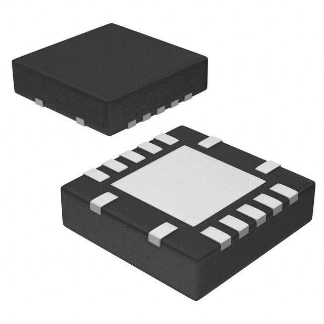
| 描述 | IC DAC 12BIT 300MSPS 48-LQFP数模转换器- DAC 12-Bit 300 MSPS High Speed |
| 产品分类 | |
| 品牌 | Analog Devices |
| 产品手册 | |
| 产品图片 |
|
| rohs | 符合RoHS无铅 / 符合限制有害物质指令(RoHS)规范要求 |
| 产品系列 | 数据转换器IC,数模转换器- DAC,Analog Devices AD9753ASTZTxDAC+® |
| 数据手册 | |
| 产品型号 | AD9753ASTZ |
| 产品培训模块 | http://www.digikey.cn/PTM/IndividualPTM.page?site=cn&lang=zhs&ptm=19145http://www.digikey.cn/PTM/IndividualPTM.page?site=cn&lang=zhs&ptm=18614http://www.digikey.cn/PTM/IndividualPTM.page?site=cn&lang=zhs&ptm=26125http://www.digikey.cn/PTM/IndividualPTM.page?site=cn&lang=zhs&ptm=26140http://www.digikey.cn/PTM/IndividualPTM.page?site=cn&lang=zhs&ptm=26150http://www.digikey.cn/PTM/IndividualPTM.page?site=cn&lang=zhs&ptm=26147 |
| 产品种类 | 数模转换器- DAC |
| 位数 | 12 |
| 供应商器件封装 | 48-LQFP(7x7) |
| 分辨率 | 12 bit |
| 包装 | 托盘 |
| 商标 | Analog Devices |
| 安装类型 | 表面贴装 |
| 安装风格 | SMD/SMT |
| 封装 | Tray |
| 封装/外壳 | 48-LQFP |
| 封装/箱体 | LQFP-48 |
| 工作温度 | -40°C ~ 85°C |
| 工厂包装数量 | 250 |
| 建立时间 | 11ns |
| 接口类型 | Parallel |
| 数据接口 | 并联 |
| 最大功率耗散 | 165 mW |
| 最大工作温度 | + 85 C |
| 最小工作温度 | - 40 C |
| 标准包装 | 1 |
| 电压参考 | Internal, External |
| 电压源 | 模拟和数字 |
| 电源电压-最大 | 3.6 V |
| 电源电压-最小 | 3 V |
| 积分非线性 | +/- 1.5 LSB |
| 稳定时间 | 11 ns |
| 系列 | AD9753 |
| 结构 | Segment |
| 转换器数 | 1 |
| 转换器数量 | 1 |
| 输出数和类型 | 2 电流,单极2 电流,双极 |
| 输出类型 | Current |
| 配用 | /product-detail/zh/AD9753-EB/AD9753-EB-ND/621768 |
| 采样比 | 300 MSPs |
| 采样率(每秒) | 300M |


PDF Datasheet 数据手册内容提取
12-Bit, 300 MSPS High Speed TxDAC+® D/A Converter AD9753* FEATURES FUNCTIONAL BLOCK DIAGRAM 12-Bit Dual Muxed Port DAC 300 MSPS Output Update Rate DVDD DCOM AVDD ACOM Excellent SFDR and IMD Performance SInFtDerRn atol CNloyqcku iDsto @ub l2i5n gM PHLzL Output: 69 dB PORT1 LATCH TCH IOUTA A MUX L DAC Differential or Single-Ended Clock Input C On-Chip 1.2 V Reference PORT2 LATCH DA IOUTB Single 3.3 V Supply Operation CLK+ Power Dissipation: 155mW @ 3.3 V REFIO CLK– PLL REFERENCE 48-Lead LQFP CLKVDD CLOCK FSADJ PLLVDD MULTIPLIER APPLICATIONS CLKCOM AD9753 Communications: LMDS, LMCS, MMDS RESET LPF DIV0 DIV1 PLLLOCK Base Stations Digital Synthesis QAM and OFDM GENERAL DESCRIPTION The DAC utilizes a segmented current source architecture The AD9753 is a dual, muxed port, ultrahigh speed, single- combined with a proprietary switching technique to reduce channel, 12-bit CMOS DAC. It integrates a high quality 12-bit glitch energy and to maximize dynamic accuracy. Differential TxDAC+ core, a voltage reference, and digital interface circuitry current outputs support single-ended or differential applica- into a small 48-lead LQFP package. The AD9753 offers excep- tions. The differential outputs each provide a nominal full-scale tional ac and dc performance while supporting update rates up current from 2 mA to 20 mA. to 300 MSPS. The AD9753 is manufactured on an advanced low cost 0.35 µm The AD9753 has been optimized for ultrahigh speed applica- CMOS process. It operates from a single supply of 3.0 V to 3.6 V tions up to 300 MSPS where data rates exceed those possible on and consumes 155 mW of power. a single data interface port DAC. The digital interface consists of two buffered latches as well as control logic. These latches PRODUCT HIGHLIGHTS can be time multiplexed to the high speed DAC in several ways. 1. The AD9753 is a member of a pin compatible family of high This PLL drives the DAC latch at twice the speed of the exter- speed TxDAC+s providing 10-, 12-, and 14-bit resolution. nally applied clock and is able to interleave the data from the 2. Ultrahigh Speed 300 MSPS Conversion Rate. two input channels. The resulting output data rate is twice that 3. Dual 12-Bit Latched, Multiplexed Input Ports. The AD9753 of the two input channels. With the PLL disabled, an external features a flexible digital interface allowing high speed data 2× clock may be supplied and divided by two internally. conversion through either a single or dual port input. 4. Low Power. Complete CMOS DAC function operates on The CLK inputs (CLK+/CLK–) can be driven either differen- 155 mW from a 3.0 V to 3.6 V single supply. The DAC full- tially or single-ended, with a signal swing as low as 1 V p-p. scale current can be reduced for lower power operation. 5. On-Chip Voltage Reference. The AD9753 includes a 1.20 V temperature-compensated band gap voltage reference. *Protected by U.S. Patent numbers 5450084, 5568145, 5689257, and 5703519. REV.B Information furnished by Analog Devices is believed to be accurate and reliable. However, no responsibility is assumed by Analog Devices for its use, nor for any infringements of patents or other rights of third parties that may result from its use. No license is granted by implication or otherwise One Technology Way, P.O. Box 9106, Norwood, MA 02062-9106, U.S.A. under any patent or patent rights of Analog Devices. Trademarks and Tel: 781/329-4700 www.analog.com registered trademarks are the property of their respective companies. Fax: 781/326-8703 © 2003 Analog Devices, Inc. All rights reserved.
AD9753–SPECIFICATIONS (T to T , AVDD = 3.3 V, DVDD = 3.3 V, PLLVDD = 3.3 V, CLKVDD = 3.3 V, I = 20 mA, unless DC SPECIFICATIONS MIN MAX OUTFS otherwise noted.) Parameter Min Typ Max Unit RESOLUTION 12 Bits DC ACCURACY1 Integral Linearity Error (INL) –1.5 ±0.5 +1.5 LSB Differential Nonlinearity (DNL) –1 ±0.4 +1 LSB ANALOG OUTPUT Offset Error –0.025 ±0.01 +0.025 % of FSR Gain Error (Without Internal Reference) –2 ±0.5 +2 % of FSR Gain Error (With Internal Reference) –2 ±0.25 +2 % of FSR Full-Scale Output Current2 2.0 20.0 mA Output Compliance Range –1.0 +1.25 V Output Resistance 100 kΩ Output Capacitance 5 pF REFERENCE OUTPUT Reference Voltage 1.14 1.20 1.26 V Reference Output Current3 100 nA REFERENCE INPUT Input Compliance Range 0.1 1.25 V Reference Input Resistance 1 MΩ TEMPERATURE COEFFICIENTS Offset Drift 0 ppm of FSR/°C Gain Drift (Without Internal Reference) ±50 ppm of FSR/°C Gain Drift (With Internal Reference) ±100 ppm of FSR/°C Reference Voltage Drift ±50 ppm/°C POWER SUPPLY Supply Voltages AVDD 3.0 3.3 3.6 V DVDD 3.0 3.3 3.6 V PLLVDD 3.0 3.3 3.6 V CLKVDD 3.0 3.3 3.6 V Analog Supply Current (I )4 33 36 mA AVDD Digital Supply Current (I )4 3.5 4.5 mA DVDD PLL Supply Current (I )4 4.5 5.1 mA PLLVDD Clock Supply Current (I )4 10.0 11.5 mA CLKVDD Power Dissipation4 (3 V, I = 20 mA) 155 165 mW OUTFS Power Dissipation5 (3 V, I = 20 mA) 216 mW OUTFS Power Supply Rejection Ratio6—AVDD –1 +1 % of FSR/V Power Supply Rejection Ratio6—DVDD –0.04 +0.04 % of FSR/V OPERATING RANGE –40 +85 °C NOTES 1Measured at I , driving a virtual ground. OUTA 2Nominal full-scale current, I , is 32× the I current. OUTFS REF 3An external buffer amplifier is recommended to drive any external load. 4100 MSPS f with PLL on, f = 1 MHz, all supplies = 3.0 V. DAC OUT 5300 MSPS f . DAC 6±5% power supply variation. Specifications subject to change without notice. –2– REV.B
AD9753 (T to T , AVDD = 3.3 V, DVDD = 3.3 V, PLLVDD = 0 V, CLKVDD = 3.3 V, I = 20 mA, DYNAMIC SPECIFICATIONS MIN MAX OUTFS Differential Transformer-Coupled Output, 50 V Doubly Terminated, unless otherwise noted.) Parameter Min Typ Max Unit DYNAMIC PERFORMANCE Maximum Output Update Rate (f ) 300 MSPS DAC Output Settling Time (t ) (to 0.1%)1 11 ns ST Output Propagation Delay (t )1 1 ns PD Glitch Impulse1 5 pV-s Output Rise Time (10% to 90%)1 2.5 ns Output Fall Time (10% to 90%)1 2.5 ns Output Noise (I = 20 mA) 50 pA/√Hz OUTFS Output Noise (I = 2 mA) 30 pA/√Hz OUTFS AC LINEARITY Spurious-Free Dynamic Range to Nyquist f = 100 MSPS; f = 1.00 MHz DAC OUT 0 dBFS Output 72 82 dBc –6 dBFS Output 76 dBc –12 dBFS Output 76 dBc f = 65 MSPS; f = 1.1 MHz2 77 dBc DATA OUT f = 65 MSPS; f = 5.1 MHz2 77 dBc DATA OUT f = 65 MSPS; f = 10.1 MHz2 76 dBc DATA OUT f = 65 MSPS; f = 20.1 MHz2 72 dBc DATA OUT f = 65 MSPS; f = 30.1 MHz2 68 dBc DATA OUT f = 200 MSPS; f = 1.1 MHz 78 dBc DAC OUT f = 200 MSPS; f = 11.1 MHz 75 dBc DAC OUT f = 200 MSPS; f = 31.1 MHz 70 dBc DAC OUT f = 200 MSPS; f = 51.1 MHz 70 dBc DAC OUT f = 200 MSPS; f = 71.1 MHz 67 dBc DAC OUT f = 300 MSPS; f = 1.1 MHz 78 dBc DAC OUT f = 300 MSPS; f = 26.1 MHz 69 dBc DAC OUT f = 300 MSPS; f = 51.1 MHz 65 dBc DAC OUT f = 300 MSPS; f = 101.1 MHz 59 dBc DAC OUT f = 300 MSPS; f = 141.1 MHz 58 dBc DAC OUT Spurious-Free Dynamic Range within a Window f = 100 MSPS; f = 1 MHz; 2 MHz Span DAC OUT 0 dBFS Output 82.5 92 dBc f = 65 MSPS; f = 5.02 MHz; 2 MHz Span 85 dBc DAC OUT f = 150 MSPS; f = 5.04 MHz; 4 MHz Span 85 dBc DAC OUT Total Harmonic Distortion f = 100 MSPS; f = 1.00 MHz DAC OUT 0 dBFS –82 –71 dBc f = 65 MHz; f = 2.00 MHz –76 dBc DAC OUT f = 160 MHz; f = 2.00 MHz –76 dBc DAC OUT Multitone Power Ratio (Eight Tones at 110 kHz Spacing) f = 65 MSPS; f = 2.00 MHz to 2.77 MHz DAC OUT 0 dBFS Output 73 dBc –6 dBFS Output 71 dBc –12 dBFS Output 69 dBc NOTES 1Measured single-ended into 50 Ω load. 2Single-Port Mode (PLL disabled, DIV0 = 1, DIV1 = 0, data on Port 1). Specifications subject to change without notice. REV. B –3–
AD9753 DIGITAL SPECIFICATIONS (T to T , AVDD = DVDD = PLLVDD = CLKVDD = 3.3 V, I = 20 mA, unless otherwise noted.) MIN MAX OUTFS Parameter Min Typ Max Unit DIGITAL INPUTS Logic 1 2.1 3 V Logic 0 0 0.9 V Logic 1 Current –10 +10 µA Logic 0 Current –10 +10 µA Input Capacitance 5 pF Input Setup Time (t ), T = 25°C 1.0 0.5 ns S A Input Hold Time (t ), T = 25°C 1.0 0.5 ns H A Latch Pulsewidth (t ), T = 25°C 1.5 ns LPW A Input Setup Time (t , PLLVDD = 0 V), T = 25°C –1.0 –1.5 ns S A Input Hold Time (t , PLLVDD = 0 V), T = 25°C 2.5 1.7 ns H A CLK to PLLLOCK Delay (t , PLLVDD = 0 V), T = 25°C 3.5 4.0 ns D A Latch Pulsewidth (t PLLVDD = 0 V), T = 25°C 1.5 ns LPW A PLLOCK (V ) 3.0 V OH PLLOCK (V ) 0.3 V OL CLK INPUTS Input Voltage Range 0 3 V Common-Mode Voltage 0.75 1.5 2.25 V Differential Voltage 0.5 1.5 V Min CLK Frequency* 6.25 MHz *Min CLK Frequency applies only when using internal PLL. When PLL is disabled, there is no minimum CLK frequency. Specifications subject to change without notice. –4– REV. B
AD9753 ABSOLUTE MAXIMUM RATINGS* Parameter With Respect to Min Max Unit AVDD, DVDD, CLKVDD, PLLVDD ACOM, DCOM, CLKCOM, PLLCOM –0.3 +3.9 V AVDD, DVDD, CLKVDD, PLLVDD AVDD, DVDD, CLKVDD, PLLVDD –3.9 +3.9 V ACOM, DCOM, CLKCOM, PLLCOM ACOM, DCOM, CLKCOM, PLLCOM –0.3 +0.3 V REFIO, REFLO, FSADJ ACOM –0.3 AVDD + 0.3 V I , I ACOM –1.0 AVDD + 0.3 V OUTA OUTB Digital Data Inputs (DB13 to DB0) DCOM –0.3 DVDD + 0.3 V CLK+/CLK–, PLLLOCK CLKCOM –0.3 CLKVDD + 0.3 V DIV0, DIV1, RESET CLKCOM –0.3 CLKVDD + 0.3 V LPF PLLCOM –0.3 PLLVDD + 0.3 V Junction Temperature 150 °C Storage Temperature –65 +150 °C Lead Temperature (10 sec) 300 °C *Stresses above those listed under Absolute Maximum Ratings may cause permanent damage to the device. This is a stress rating only; functional operation of the device at these or any other conditions above those indicated in the operational sections of this specification is not implied. Exposure to absolute maximum ratings for extended periods may affect device reliability. ORDERING GUIDE t t S H Temperature Package Package PORT 1 DATA X Model Range Description Option DATA IN AD9753AST –40°C to +85°C 48-Lead LQFP ST-48 PORT 2 DATA Y AD9753ASTRL –40°C to +85°C 48-Lead LQFP ST-48 AD9753-EB Evaluation INPUT CLK Board (PLL ENABLED) t t LPW PD IOUTA OR IOUTB DATA X DATA Y THERMAL CHARACTERISTIC Thermal Resistance t PD 48-Lead LQFP (cid:1) = 91°C/W JA Figure 1.I/O Timing CAUTION ESD (electrostatic discharge) sensitive device. Electrostatic charges as high as 4000 V readily accumulate on the human body and test equipment and can discharge without detection. Although the AD9753 features proprietary ESD protection circuitry, permanent damage may occur on devices subjected to high energy electrostatic discharges. Therefore, proper ESD precautions are recommended to avoid performance degradation or loss of functionality. REV. B –5–
AD9753 PIN CONFIGURATION CLKVDD PLLVDD LPF CLKCOM ACOM IOUTAIOUTBAVDD FSADJ REFIO DIV1 DIV0 48 47 46 45 44 43 42 41 40 39 38 37 RESET 1 36 RESERVED PIN 1 CLK+ 2 IDENTIFIER 35 RESERVED CLK– 3 34 P2B0–LSB DCOM 4 33 P2B1 DVDD 5 32 P2B2 AD9753 PLLLOCK 6 31 P2B3 MSB–P1B11 7 (NToOt Pto V SIEcaWle) 30 P2B4 P1B10 8 29 P2B5 P1B9 9 28 P2B6 P1B8 10 27 P2B7 P1B7 11 26 P2B8 P1B6 12 25 P2B9 13 14 15 16 17 18 19 20 21 22 23 24 5 4 3 2 1 0 D D D M 1 0 P1B P1B P1B P1B P1B LSB–P1B RESERVE RESERVE DVD DCO MSB–P2B1 P2B1 RUESSEERR CVOENDN =E NCOTIONS PIN FUNCTION DESCRIPTIONS Pin No. Mnemonic Description 1 RESET Internal Clock Divider Reset 2 CLK+ Differential Clock Input 3 CLK– Differential Clock Input 4, 22 DCOM Digital Common 5, 21 DVDD Digital Supply Voltage 6 PLLLOCK Phase-Locked Loop Lock Indicator Output 7–18 P1B11–P1B0 Data Bits DB11 to DB0, Port 1 19–20, 35–36 RESERVED 23–34 P2B11–P2B0 Data Bits DB11 to DB0, Port 2 37, 38 DIV0, DIV1 Control Inputs for PLL and Input Port Selector Mode. See Tables I and II for details. 39 REFIO Reference Input/Output 40 FSADJ Full-Scale Current Output Adjust 41 AVDD Analog Supply Voltage 42 I Differential DAC Current Output OUTB 43 I Differential DAC Current Output OUTA 44 ACOM Analog Common 45 CLKCOM Clock and Phase-Locked Loop Common 46 LPF Phase-Locked Loop Filter 47 PLLVDD Phase-Locked Loop Supply Voltage 48 CLKVDD Clock Supply Voltage –6– REV. B
AD9753 TERMINOLOGY Power Supply Rejection Linearity Error (Also Called Integral Nonlinearity or INL) The maximum change in the full-scale output as the supplies Linearity error is defined as the maximum deviation of the actual are varied from minimum to maximum specified voltages. analog output from the ideal output, determined by a straight Settling Time line drawn from zero to full scale. The time required for the output to reach and remain within a Differential Nonlinearity (DNL) specified error band about its final value, measured from the DNL is the measure of the variation in analog value, normalized start of the output transition. to full scale, associated with a 1 LSB change in digital input code. Glitch Impulse Monotonicity Asymmetrical switching times in a DAC give rise to undesired A D/A converter is monotonic if the output either increases or output transients that are quantified by a glitch impulse. It is remains constant as the digital input increases. specified as the net area of the glitch in pV-s. Offset Error Spurious-Free Dynamic Range The deviation of the output current from the ideal of zero is The difference, in dB, between the rms amplitude of the output called offset error. For I , 0 mA output is expected when the signal and the peak spurious signal over the specified bandwidth. OUTA inputs are all 0s. For I , 0 mA output is expected when all OUTB Total Harmonic Distortion (THD) inputs are set to 1s. THD is the ratio of the rms sum of the first six harmonic com- Gain Error ponents to the rms value of the measured fundamental. It is The difference between the actual and ideal output span. The expressed as a percentage or in decibels (dB). actual span is determined by the output when all inputs are set Signal-to-Noise Ratio (SNR) to 1s, minus the output when all inputs are set to 0s. SNR is the ratio of the rms value of the measured output signal Output Compliance Range to the rms sum of all other spectral components below the Nyquist The range of allowable voltage at the output of a current-output frequency, excluding the first six harmonics and dc. The value DAC. Operation beyond the maximum compliance limits may for SNR is expressed in decibels. cause either output stage saturation or breakdown, resulting in Adjacent Channel Power Ratio (ACPR) nonlinear performance. A ratio in dBc between the measured power within a channel Temperature Drift relative to its adjacent channel. Specified as the maximum change from the ambient (25°C) value to the value at either T or T . For offset and gain MIN MAX drift, the drift is reported in ppm of full-scale range (FSR) per degree Celsius. For reference drift, the drift is reported in ppm per degree Celsius. 3.0V TO 3.6V MINI TO ROHDE & DVDD AVDD CIRCUITS SCHWARZ REF1IO.2V REF SPMOUORSC CEU ARRRREANYT SDSWBEITG0C MTHOEE NDSTB FE1OD1R DAC IIOOUUTTAB 50(cid:2) T1-1T FSASPNEEAACL3TY0RZEURM 0.1(cid:1)F FSADJ PLLVDD R2SkE(cid:2)T D2A–C1 L MAUTCXH CIRCPULLITRY CRLPLEFKSVEDTD 50(cid:2) AD9753 CLKCOM DCOM DIV0 PORT 1 LATCH PORT 2 LATCH DIV1 ACOM DB0 – DB11 DB0 – DB11 CLK+ CLK– PLLLOCK DIGITAL DATA INPUTS 1k(cid:2) 3.0V TO 3.6V TEKTRONIX DG2020 MINI 1k(cid:2) OR CIRCUITS AWG2021 w/OPTION 4 T1-1T LECROY 9210 HP8644 PULSE GENERATOR SIGNAL (FOR DATA RETIMING) GENERATOR PLL DISABLED PLL ENABLED Figure 2.Basic AC Characterization Test Setup REV. B –7–
AD9753–Typical Performance Characteristics 90 90 90 0dBmFS 80 80 80 0dBmFS –6dBmFS R (dBc) 70 –6dBmFS R (dBc) 70 R (dBc) 70 –6dBmFS D D D SF 60 –12dBmFS SF 60 –12dBmFS SF 60 0dBmFS 50 50 50 –12dBmFS 40 40 40 0 5 10 15 20 25 30 35 0 10 20 30 40 50 60 70 80 90 100 0 20 40 60 80 100 120 140 160 fOUT (MHz) fOUT (MHz) fOUT (MHz) TPC 1.Single-Tone SFDR vs. f @ TPC 2.Single-Tone SFDR vs. TPC 3.Single-Tone SFDR vs. OUT fDAC = 65 MSPS, Single-Port Mode fOUT @ fDAC = 200 MSPS fOUT @ fDAC = 300 MSPS 90 90 90 SFDR NEAR CARRIERS (2F1-F2, 2F2-F1) 80 80 80 SFDR CLOSE TO CARRIERS (2F1-F2, 2F2-F1) 200MSPS Bc) 70 Bc) 70 SFDR OVER Bc) 70 R (d R (d NYQUIST BAND R (d D D D SF 60 SF 60 SF 60 65MSPS 50 300MSPS 50 50 SFDR OVER NYQUIST BAND 40 40 40 0 20 40 60 80 100 120 140 0 10 20 30 40 50 60 70 80 90 100 0 20 40 60 80 100 120 140 160 fOUT (MHz) fOUT (MHz) fOUT (MHz) TPC 4.SFDR vs. fOUT @ 0 dBFS TPC 5.Two-Tone IMD vs. fOUT @ TPC 6.Two-Tone IMD vs. fOUT @ fDAC = 200 MSPS, 1 MHz Spacing fDAC = 300 MSPS, 1 MHz Spacing between Tones, 0 dBFS between Tones, 0 dBFS 90 90 11.82MHz @ 130MSPS 90 26MHz @ 130MSPS 80 80 80 11.82MHz/12.82MHz 18.18MHz @ 200MSPS @ 130MSPS Bc) 70 Bc) 70 Bc) 70 R (d R (d 40MHz @ 200MSPS R (d 18.18MHz/19.18MHz D D D @ 200MSPS SF 60 SF 60 SF 60 27.27MHz @ 300MSPS 27.27MHz/28.27MHz @ 300MSPS 50 50 50 60MHz @ 300MSPS 40 40 40 –16 –14 –12 –10 –8 –6 –4 –2 0 –16 –14 –12 –10 –8 –6 –4 –2 0 –20–18–16–14–12 –10 –8 –6 –4 –2 0 AOUT (dB) AOUT (dBm) AOUT (dBm) TPC 7.Single-Tone SFDR vs. TPC 8.Single-Tone SFDR vs. TPC 9.Two-Tone IMD (Third Order AOUT @ fOUT = fDAC/11 AOUT @ fOUT = fDAC/5 Products) vs. AOUT @ fOUT = fDAC/11 –8– REV. B
AD9753 90 90 90 11.82MHz/12.82MHz @ 130MSPS 40MHz/41MHz 26MHz/27MHz @ 200MSPS @ 130MSPS 80 80 26MHz/27MHz 80 @ 130MSPS dBc) 70 18.18MHz/19.18MHz dBc) 70 dBc) 70 R ( @ 200MSPS R ( R ( D D 60MHz/61MHz D 40MHz/41MHz SF 60 SF 60 @ 300MSPS SF 60 @ 200MSPS 27.27MHz/28.27MHz 50 @ 300MSPS 50 50 60MHz/61MHz @ 300MSPS 40 40 40 –20–18–16–14–12 –10 –8 –6 –4 –2 0 –20–18–16–14–12 –10 –8 –6 –4 –2 0 –20–18–16–14–12 –10 –8 –6 –4 –2 0 AOUT (dBm) AOUT (dBm) AOUT (dBm) TPC 10.Two-Tone IMD (to Nyquist) TPC 11.Two-Tone IMD (Third Order TPC 12.Two-Tone IMD (to Nyquist) vs. AOUT @ fOUT = fDAC/11 Products) vs. AOUT @ fOUT = fDAC/5 vs. AOUT @ fOUT = fDAC/5 80 90 75 75 85 70 70 10MHz 80 65 SINAD (dBm) 767055 SFDR (dBc) 6505 IOUTFS I=O U2T0FmSA = 10mA SFDR (dBc) 665505 4800MMHHzz 50 IOUTFS = 5mA 60 50 55 45 45 120MHz 50 40 40 50 100 150 200 250 300 0 20 40 60 80 100 120 140 160 –50 –30 –10 10 30 50 70 90 fDAC (MHz) fOUT (MHz) TEMPERATURE ((cid:3)C) TPC 13.SINAD vs. f @ TPC 14.SFDR vs. I , f = TPC 15.SFDR vs. Temperature, DAC OUTFS DAC fOUT = 10 MHz, 0 dBFS 300 MSPS @ 0 dBFS fDAC = 300 MSPS @ 0 dBFS 0.1 0.54 0.6 0.50 0 0.46 –10 fDAC = 300MSPS fOUT1 = 24MHz 0.4 0.42 –20 fOUT2 = 25MHz L (LSB) 0.20 L (LSB) 0000....33328406 UDE (dBm) –––345000 ffffOOOOUUUUTTTT3456 ==== 22226789MMMMHHHHzzzz IN DN0.22 LIT –60 fOUT7 = 30MHz –0.2 00..1184 AMP –75 SfOFUDTR8 == 3518MdBHcz MAGNITUDE = 0dBFS 0.10 –80 –0.4 0.06 –95 0.02 –0.6 –0.02 –100 0 511 1023153520472559307135834095 0 511 1023153520472559307135834095 0 20 40 60 80 100 120 1400 CODE CODE FREQUENCY (MHz) TPC 16.Typical INL TPC 17.Typical DNL TPC 18.Eight-Tone SFDR @ f ≈ OUT f /11, f = 300 MSPS DAC DAC REV. B –9–
AD9753 3.0V TO 3.6V VDIFF = VOUTA – VOUTB DVDD AVDD REF1IO.2V REF PSMOUORSC CEU ARRRREANYT SDSWBEITG0C MTHOEE NDSTB FE1OD1R DAC IIOOUUTTAB VOUTB RVOLOUATDA 0.1(cid:1)F R2SkE(cid:2)T FSADJ DAC LATCH PLL PCCLLLLKKVV+DDDD R50L(cid:2)OAD 50(cid:2) 2–1 MUX CIRCUITRY CLK– AD9753 CLKCOM DCOM RESET PORT 1 LATCH PORT 2 LATCH LPF ACOM DB0 – DB11 DB0 – DB11 DIV0DIV1PLLLOCK DIGITAL DATA INPUTS Figure 3.Simplified Block Diagram FUNCTIONAL DESCRIPTION REFERENCE OPERATION Figure 3 shows a simplified block diagram of the AD9753. The The AD9753 contains an internal 1.20 V band gap reference. AD9753 consists of a PMOS current source array capable of This can easily be overdriven by an external reference with no providing up to 20 mA of full-scale current, I . The effect on performance. REFIO serves as either an input or output, OUTFS array is divided into 31 equal sources that make up the five depending on whether the internal or an external reference is most significant bits (MSBs). The next four bits, or middle bits, used. To use the internal reference, simply decouple the REFIO consist of 15 equal current sources whose value is 1/16th of an pin to ACOM with a 0.1 µF capacitor. The internal reference MSB current source. The remaining LSBs are a binary weighted voltage will be present at REFIO. If the voltage at REFIO is to fraction of the middle bit current sources. Implementing the be used elsewhere in the circuit, an external buffer amplifier middle and lower bits with current sources, instead of an R-2R with an input bias current less than 100 nA should be used. An ladder, enhances dynamic performance for multitone or low example of the use of the internal reference is given in Figure 4. amplitude signals and helps maintain the DAC’s high output A low impedance external reference can be applied to REFIO, impedance (i.e., >100 kΩ). as shown in Figure 5. The external reference may provide either All of the current sources are switched to one of the two a fixed reference voltage to enhance accuracy and drift perfor- outputs (i.e., I or I ) via PMOS differential current mance or a varying reference voltage for gain control. Note OUTA OUTB switches. The switches are based on a new architecture that that the 0.1 µF compensation capacitor is not required since drastically improves distortion performance. This new switch the internal reference is overdriven, and the relatively high input architecture reduces various timing errors and provides matching impedance of REFIO minimizes any loading of the external complementary drive signals to the inputs of the differential reference. current switches. The analog and digital sections of the AD9753 have separate EOXPTTEIORNNAALL AD9753 AVDD power supply inputs (i.e., AVDD and DVDD) that can operate REFERENCE REFERENCE BUFFER SECTION independently over a 3.0 V to 3.6 V range. The digital section, 1.2V REF which is capable of operating at a 300 MSPS clock rate, consists REFIO of edge-triggered latches and segment decoding logic circuitry. ADDITIONAL CURRENT The analog section includes the PMOS current sources, the EXTERNAL 0.1(cid:1)F FSADJ SOURCE LOAD ARRAY associated differential switches, a 1.20 V band gap voltage refer- IREF 2k(cid:2) ence, and a reference control amplifier. The full-scale output current is regulated by the reference control Figure 4.Internal Reference Configuration amplifier and can be set from 2 mA to 20 mA via an external resistor, R . The external resistor, in combination with both SET the reference control amplifier and voltage reference VREFIO, sets AD9753 AVDD the reference current I , which is replicated to the segmented REFERENCE REF AVDD SECTION current sources with the proper scaling factor. The full-scale 1.2V REF current, I , is 32 times the value of I . OUTFS REF EXTERNAL REFIO CURRENT REFERENCE FSADJ SOURCE ARRAY IREF 2k(cid:2) Figure 5.External Reference Configuration –10– REV. B
AD9753 REFERENCE CONTROL AMPLIFIER t t S H The AD9753 also contains an internal control amplifier that is used to regulate the DAC’s full-scale output current, IOUTFS. PORT 1 DATA X The control amplifier is configured as a voltage-to-current DATA IN converter as shown in Figure 4, so that its current output, I , is REF PORT 2 DATA Y determined by the ratio of V and an external resistor, R , REFIO SET as stated in Equation 4. I is applied to the segmented current REF sources with the proper scaling factor to set IOUTFS, as stated in CLK Equation 3. tLPW tPD TI he co novtreorl aa m2 pmliAfi etro a2ll0o wmsA a rwanidgee (b1y0 s:1et)t iandgj uIstm ebnett wspeaenn of IOUTA OR IOUTB DATA X DATA Y OUTFS REF 62.5 µA and 625 µA. The wide adjustment span of IOUTFS 1/2 CYCLE + tPD provides several application benefits. The first benefit relates Figure 7a. DAC Input Timing Requirements with directly to the power dissipation of the AD9753, which is PLL Active, Single Clock Cycle proportional to I (refer to the Power Dissipation section). OUTFS The second benefit relates to the 20 dB adjustment, which is useful for system gain control purposes. PORT 1 DATA W DATA Y The small signal bandwidth of the reference control amplifier is DATA IN approximately 500 kHz and can be used for low frequency, PORT 2 DATA X DATA Z small signal multiplying applications. CLK PLL CLOCK MULTIPLIER OPERATION The Phase-Locked Loop (PLL) is intrinsic to the operation of the AD9753 in that it produces the necessary internally syn- XXX chronized 2× clock for the edge-triggered latches, multiplexer, IOUTA OR IOUTB DATA W DATA X and DAC. DATA Y DATA Z With PLLVDD connected to its supply voltage, the AD9753 is Figure 7b.DAC Input Timing Requirements with in PLL mode. Figure 6 shows a functional block diagram of the PLL Active, Multiple Clock Cycles AD9753 clock control circuitry with PLL active. The circuitry consists of a phase detector, charge pump, voltage controlled Typically, the VCO can generate outputs of 100 MHz to oscillator (VCO), input data rate range control, clock logic 400 MHz. The range control is used to keep the VCO operating circuitry, and control input/outputs. The ÷2 logic in the feed- within its designed range, while allowing input clocks as low as back loop allows the PLL to generate the 2× clock needed for 6.25 MHz. With the PLL active, logic levels at DIV0 and DIV1 the DAC output latch. determine the divide (prescaler) ratio of the range controller. Table I gives the frequency range of the input clock for the different states of DIV0 and DIV1. 392(cid:2) 1.0(cid:1)F 3.0V TO CLKVDD 3.6V (3.0V TO 3.6V) PLLLOCK LPF PLLVDD Table I. CLK Rates for DIV0, DIV1 Levels with PLL Active CLK Frequency DIV1 DIV0 Range Controller SDIINFFGEL RETEO-EN-NTDIAELD- DEPTHEACSTEOR CHPUAMRGPE VCO 50 MHz–150 MHz 0 0 ÷1 AMP RANGE DIV0 25 MHz–100 MHz 0 1 ÷2 CLK+ CONTROL CLK– ((cid:4)1, 2, 4, 8) DIV1 12.5 MHz–50 MHz 1 0 ÷4 TO INPUT (cid:4)2 6.25 MHz–25 MHz 1 1 ÷8 LATCHES TO DAC AD9753 LATCH A 392 Ω resistor and 1.0 µF capacitor connected in series from CLKCOM LPF to PLLVDD are required to optimize the phase noise versus the settling/acquisition time characteristics of the PLL. To Figure 6.Clock Circuitry with PLL Active obtain optimum noise and distortion performance, PLLVDD Figure 7 defines the input and output timing for the AD9753 should be set to a voltage level similar to DVDD and with the PLL active. CLK in Figure 7 represents the clock CLKVDD. that is generated external to the AD9753. The input data at In general, the best phase noise performance for any PLL range both Ports 1 and 2 is latched on the same CLK rising edge. control setting is achieved with the VCO operating near its maxi- CLK may be applied as a single-ended signal by tying CLK– to mum output frequency of 400 MHz. midsupply and applying CLK to CLK+, or as a differential signal applied to CLK+ and CLK–. As stated earlier, applications requiring input data rates below 6.25 MSPS must disable the PLL clock multiplier and provide RESET has no purpose when using the internal PLL and should an external 2× reference clock. At higher data rates however, be grounded. When the AD9753 is in PLL mode, PLLLOCK applications already containing a low phase noise (i.e., jitter) is the output of the internal phase detector. When locked, the lock output in this mode will be a Logic 1. REV. B –11–
AD9753 reference clock that is twice the input data rate should consider Following the rising edge of CLK at a time equal to half of its disabling the PLL clock multiplier to achieve the best SNR period, the data in the Port 1 latch will be written to the DAC performance from the AD9753. Note, the SFDR performance output latch, again with a corresponding change in the DAC of the AD9753 remains unaffected with or without the PLL output. Due to the internal PLL, the time at which the data in clock multiplier enabled. the Port 1 and Port 2 input latches is written to the DAC latch is independent of the duty cycle of CLK. When using the PLL, The effects of phase noise on the AD9753’s SNR performance the external clock can be operated at any duty cycle that meets become more noticeable at higher reconstructed output frequen- the specified input pulsewidth. cies and signal levels. Figure 8 compares the phase noise of a full-scale sine wave at exactly f /4 at different data rates On the next rising edge of CLK, the cycle begins again with the DATA (thus carrier frequency) with the optimum DIV1, DIV0 setting. two input port latches being updated, and the DAC output latch being updated with the current data in the Port 2 input latch. SNR is partly a function of the jitter generated by the clock circuitry. As a result, any noise on PLLVDD or CLKVDD may PLL DISABLED MODE decrease the SNR at the output of the DAC. To minimize this When PLLVDD is grounded, the PLL is disabled. An external potential problem, PLLVDD and CLKVDD can be connected clock must now drive the CLK inputs at the desired DAC out- to DVDD using an LC filter network similar to the one shown put update rate. The speed and timing of the data present at in Figure 9. input Ports 1 and 2 are now dependent on whether or not the AD9753 is interleaving the digital input data or only responding 0 to data on a single port. Figure 10 is a functional block diagram –10 of the AD9753 clock control circuitry with the PLL disabled. –20 Hz) –30 PLLLOCK m/ B –40 TO DAC Y (d –50 AD9753 LATCH T NSI –60 CLKIN+ CLLOOGCICK TO INPUT E DE –70 PLL ON, fDATA = 150MSPS CLKIN– DIFFERENTIAL- ((cid:4)1 OR (cid:4)2) LATCHES NOIS –80 SINGLTEO-E-NDED TINOTERNAL AMP MUX –90 PLLVDD –100 RESET DIV0 DIV1 PLL OFF, fDATA = 50MSPS –110 0 1 2 3 4 5 Figure 10.Clock Circuitry with PLL Disabled FREQUENCY OFFSET (MHz) DIV0 and DIV1 no longer control the PLL but are used to set Figure 8.Phase Noise of PLL Clock Multiplier at the control on the input mux for either interleaving or non- fOUT = fDATA/4 at Different fDATA Settings with DIV0/DIV1 interleaving the input data. The different modes for states of Optimized, Using R&S FSEA30 Spectrum Analyzer DIV0 and DIV1 are given in Table II. FERRITE Table II. Input Mode for DIV0, BEADS CLKVDD DIV1 Levels with PLL Disabled 100(cid:1)F 10(cid:1)F 0.1(cid:1)F TTL/CMOS ELECT. TANT. CER. Input Mode DIV1 DIV0 LOGIC CIRCUITS PLLVDD Interleaved (2×) 0 0 Noninterleaved CLKCOM Port 1 Selected 0 1 Port 2 Selected 1 0 3.3V POWER SUPPLY Not Allowed 1 1 Figure 9.LC Network for Power Filtering DAC TIMING WITH PLL ACTIVE As described in Figure 7, in PLL active mode, Port 1 and Port 2 input latches are updated on the rising edge of CLK. On the same rising edge, data previously present in the input Port 2 latch is written to the DAC output latch. The DAC output will update after a short propagation delay (t ). PD –12– REV. B
AD9753 INTERLEAVED (2(cid:5)) MODE WITH PLL DISABLED NONINTERLEAVED MODE WITH PLL DISABLED The relationship between the internal and external clocks in this If the data at only one port is required, the AD9753 interface can mode is shown in Figure 11. A clock at the output update data operate as a simple double buffered latch with no interleaving. rate (2× the input data rate) must be applied to the CLK inputs. On the rising edge of the 1× clock, input latch 1 or 2 is updated Internal dividers then create the internal 1× clock necessary for with the present input data (depending on the state of DIV0/ the input latches. Although the input latches are updated on the DIV1). On the next rising edge, the DAC latch is updated and a rising edge of the delayed internal 1× clock, the setup-and-hold time t later, the DAC output reflects this change. Figure 13 PD times given in the Digital Specifications table are with respect to represents the AD9753 timing in this mode. the rising edge of the external 2× clock. With the PLL disabled, a load-dependent delayed version of the 1× clock is present at t t S H the PLLLOCK pin. This signal can be used to synchronize the external data. DATA IN PORT 1 OR PORT 2 t t S H 1(cid:5) CLOCK PORT 1 DATA X DATA ENTERS tLPW t DATA IN INPUT LATCHES PD ON THIS EDGE PORT 2 DATA Y IOUTA OR IOUTB XX PDOARTAT 1O OUTR EXTERNAL PORT 2 2(cid:5) CLK tLPW tPD tPD Figure 13.Timing Requirements, Noninterleaved DELAYED Mode with PLL Disabled INTERNAL 1(cid:5) CLK t D EXTERNAL DAC TRANSFER FUNCTION 1(cid:5) CLK @ PLLLOCK The AD9753 provides complementary current outputs, IOUTA and I . I will provide a near full-scale current output, IOUTA OR IOUTB DATA X DATA Y I O,U wTBhenO UaTllA bits are high (i.e., DAC CODE = 4095), while OUTFS Figure 11.Timing Requirements, Interleaved (2×) IOUTB, the complementary output, provides no current. The current output appearing at I and I is a function of Mode with PLL Disabled OUTA OUTB both the input code and I and can be expressed as OUTFS Updates to the data at input Ports 1 and 2 should be synchro- nized to the specific rising edge of the external 2× clock that IOUTA = (DAC CODE/4096) × IOUTFS (1) corresponds to the rising edge of the 1× internal clock, as shown I = (4095 – DAC CODE)/4096 × I (2) OUTB OUTFS in Figure 11. To ensure synchronization, a Logic 1 must be where DAC CODE = 0 to 4095 (i.e., decimal representation). momentarily applied to the RESET pin. Doing this and return- ing RESET to Logic 0 brings the 1× clock at PLLLOCK to a As mentioned previously, I is a function of the reference OUTFS Logic 1. On the next rising edge of the 2× clock, the 1× clock current, I , which is nominally set by a reference voltage, REF will go to Logic 0. On the second rising edge of the 2× clock, V , and an external resistor R . It can be expressed as REFIO SET the 1× clock (PLLLOCK) will again go to Logic 1, as well as I = 32 × I (3) update the data in both of the input latches. The details of this OUTFS REF are shown in Figure 12. where I = V /R (4) REF REFIO SET DATA ENTERS INPUT LATCHES ON THESE EDGES The two current outputs typically drive a resistive load directly or via a transformer. If dc coupling is required, I and I RESET OUTA OUTB should be directly connected to matching resistive loads, R , LOAD that are tied to analog common, ACOM. Note that R may LOAD PLLLOCK represent the equivalent load resistance seen by I or I OUTA OUTB as would be the case in a doubly terminated 50Ω or 75 Ω cable. EXTERNAL The single-ended voltage output appearing at the I and 2(cid:5) CLOCK OUTA I nodes is simply tRH = 1.2ns OUTB tRS = 0.2ns VOUTA = IOUTA × RLOAD (5) V = I × R (6) Figure 12.RESET Function Timing with PLL Disabled OUTB OUTB LOAD For proper synchronization, sufficient delay must be present Note that the full-scale values of V and V should not OUTA OUTB between the time RESET goes low and the rising edge of the 2× exceed the specified output compliance range to maintain clock. RESET going low must occur either at least t ns before specified distortion and linearity performance. RS the rising edge of the 2× clock, or tRH ns afterwards. In the VDIFF = (IOUTA – IOUTB) × RLOAD (7) first case, the immediately occurring CLK rising edge will cause PLLLOCK to go low. In the second case, the next CLK rising edge will toggle PLLLOCK. REV. B –13–
AD9753 Substituting the values of I , I and I , V can be As a result, maintaining I and/or I at a virtual ground OUTA OUTB, REF DIFF OUTA OUTB expressed as via an I–V op amp configuration will result in the optimum dc V = {(2 DAC CODE – 4095)/4096} × linearity. Note that the INL/DNL specifications for the AD9753 (3D2I FRF /R ) × V (8) are measured with IOUTA and IOUTB maintained at virtual ground LOAD SET REFIO via an op amp. These last two equations highlight some of the advantages of I and I also have a negative and positive voltage com- operating the AD9753 differentially. First, the differential opera- OUTA OUTB pliance range that must be adhered to in order to achieve optimum tion will help cancel common-mode error sources associated performance. The negative output compliance range of –1.0V is with I and I such as noise, distortion, and dc offsets. OUTA OUTB set by the breakdown limits of the CMOS process. Operation Second, the differential code-dependent current and subsequent beyond this maximum limit may result in a breakdown of the voltage, V , is twice the value of the single-ended voltage DIFF output stage and affect the reliability of the AD9753. output (i.e., V or V ), thus providing twice the signal OUTA OUTB power to the load. The positive output compliance range is slightly dependent on the full-scale output current, I . It degrades slightly from its Note that the gain drift temperature performance for a single- OUTFS nominal 1.25 V for an I = 20 mA to 1.00 V for an I ended (V and V ) or differential output (V ) of the OUTFS OUTFS OUTA OUTB DIFF = 2 mA. The optimum distortion performance for a single- AD9753 can be enhanced by selecting temperature tracking ended or differential output is achieved when the maximum resistors for R and R due to their ratiometric relation- LOAD SET full-scale signal at I and I does not exceed 0.5 V. ship, as shown in Equation 8. OUTA OUTB Applications requiring the AD9753’s output (i.e., V and/ OUTA or V ) to extend its output compliance range should size ANALOG OUTPUTS OUTB R accordingly. Operation beyond this compliance range The AD9753 produces two complementary current outputs, LOAD will adversely affect the AD9753’s linearity performance and I and I , that may be configured for single-ended or OUTA OUTB subsequently degrade its distortion performance. differential operation. I and I can be converted into OUTA OUTB complementary single-ended voltage outputs, V and V , OUTA OUTB DIGITAL INPUTS via a load resistor, R , as described by Equations 5 through LOAD The AD9753’s digital inputs consist of two channels of 14 data 8 in the DAC Transfer Function section. The differential voltage, input pins each and a pair of differential clock input pins. The V , existing between V and V , can also be con- DIFF OUTA OUTB 12-bit parallel data inputs follow standard straight binary coding verted to a single-ended voltage via a transformer or differential where DB13 is the most significant bit (MSB) and DB0 is the amplifier configuration. The ac performance of the AD9753 is least significant bit (LSB). I produces a full-scale output optimum and specified using a differential transformer-coupled OUTA current when all data bits are at Logic 1. I produces a output in which the voltage swing at I and I is limited OUTB OUTA OUTB complementary output with the full-scale current split between to ±0.5V. If a single-ended unipolar output is desirable, I OUTA the two outputs as a function of the input code. should be selected as the output, with I grounded. OUTB The digital interface is implemented using an edge-triggered The distortion and noise performance of the AD9753 can be master slave latch. With the PLL active or disabled, the DAC enhanced when it is configured for differential operation. The output is updated twice for every input latch rising edge, as common-mode error sources of both I and I can be OUTA OUTB shown in Figures 7 and 11. The AD9753 is designed to support significantly reduced by the common-mode rejection of a trans- an input data rate as high as 150 MSPS, giving a DAC output former or differential amplifier. These common-mode error update rate of 300 MSPS. The setup-and-hold times can also sources include even-order distortion products and noise. The be varied within the clock cycle as long as the specified mini- enhancement in distortion performance becomes more significant mum times are met. Best performance is typically achieved as the frequency content of the reconstructed waveform increases. when the input data transitions on the falling edge of a 50% This is due to the first order cancellation of various dynamic duty cycle clock. common-mode distortion mechanisms, digital feedthrough, and noise. The digital inputs are CMOS compatible with logic thresholds, V , set to approximately half the digital positive supply Performing a differential-to-single-ended conversion via a trans- THRESHOLD (DVDD) or former also provides the ability to deliver twice the reconstructed signal power to the load (i.e., assuming no source termination). VTHRESHOLD = DVDD/2 (±20%) Since the output currents of I and I are complemen- OUTA OUTB The internal digital circuitry of the AD9753 is capable of oper- tary, they become additive when processed differentially. A ating over a digital supply range of 3.0 V to 3.6 V. As a result, properly selected transformer will allow the AD9753 to provide the digital inputs can also accommodate TTL levels when DVDD the required power and voltage levels to different loads. Refer to is set to accommodate the maximum high level voltage of the the Applying the AD9753 Output Configurations section for TTL drivers V (max). A DVDD of 3.0 V to 3.6 V typically examples of various output configurations. OH ensures proper compatibility with most TTL logic families. The output impedance of I and I is determined by the Figure 14 shows the equivalent digital input circuit for the data OUTA OUTB equivalent parallel combination of the PMOS switches associ- and clock inputs. ated with the current sources and is typically 100kΩ in parallel with 5 pF. It is also slightly dependent on the output voltage (i.e., V and V ) due to the nature of a PMOS device. OUTA OUTB –14– REV. B
AD9753 DVDD Note that the clock input could also be driven via a sine wave that is centered around the digital threshold (i.e., DVDD/2) and meets the min/max logic threshold. This typically results in a DIGITAL slight degradation in the phase noise, which becomes more INPUT noticeable at higher sampling rates and output frequencies. Also, at higher sampling rates, the 20% tolerance of the digital logic threshold should be considered since it will affect the effective clock duty cycle and, subsequently, cut into the required data Figure 14.Equivalent Digital Input setup-and-hold times. The AD9753 features a flexible differential clock input operat- ing from separate supplies (i.e., CLKVDD, CLKCOM) to INPUT CLOCK AND DATA TIMING RELATIONSHIP achieve optimum jitter performance. The two clock inputs, SNR in a DAC is dependent on the relationship between the CLK+ and CLK–, can be driven from a single-ended or differ- position of the clock edges and the point in time at which the ential clock source. For single-ended operation, CLK+ should input data changes. The AD9753 is rising edge triggered, and be driven by a logic source while CLK– should be set to the so exhibits SNR sensitivity when the data transition is close to threshold voltage of the logic source. This can be done via a this edge. In general, the goal when applying the AD9753 is to resistor divider/capacitor network, as shown in Figure 15a. For make the data transition close to the falling clock edge. This differential operation, both CLK+ and CLK– should be biased to becomes more important as the sample rate increases. Figure 16 CLKVDD/2 via a resistor divider network, as shown in Figure 15b. shows the relationship of SNR to clock placement with different sample rates. Note that the setup-and-hold times implied in Figure 16 appear to violate the maximums stated in the Digital RSERIES AD9753 Specifications of this data sheet. The variation in Figure 16 is CLK+ due to the skew present between data bits inherent in the digital CLKVDD data generator used to perform these tests. Figure 16 is presented to show the effects of violating setup-and-hold times and to 0.1(cid:1)F CLK– show the insensitivity of the AD9753 to clock placement when data transitions fall outside of the so-called “bad window.” The VTHRESHOLD CLKCOM setup-and-hold times stated in the Digital Specifications table were measured on a bit-by-bit basis, therefore eliminating the Figure 15a.Single-Ended Clock Interface skew present in the digital data generator. At higher data rates, it becomes very important to account for the skew in the input digital data when defining timing specifications. 0.1(cid:1)F AD9753 CLK+ 0.1(cid:1)F 80 CLKVDD 0.1(cid:1)F 70 CLK– 60 CLKCOM 50 c) Figure 15b.Differential Clock Interface dB R ( 40 Because the output of the AD9753 can be updated at up to N S 30 300 MSPS, the quality of the clock and data input signals is important in achieving the optimum performance. The drivers 20 of the digital data interface circuitry should be specified to meet the minimum setup-and-hold times of the AD9753 as 10 well as its required min/max input logic level thresholds. 0 Digital signal paths should be kept short and run lengths matched –3 –2 –1 0 1 2 3 to avoid propagation delay mismatch. Inserting a low value resis- TIME OF DATA TRANSITION RELATIVE TO PLACEMENT OF CLK RISING EDGE (ns), fOUT = 10MHz, fDAC = 300MHz tor network (i.e., 20 Ω to 100 Ω) between the AD9753 digital Figure 16.SNR vs. Time of Data Transition inputs and driver outputs may be helpful in reducing any over- Relative to Clock Rising Edge shooting and ringing at the digital inputs that contribute to data feedthrough. For longer run lengths and high data update rates, POWER DISSIPATION strip line techniques with proper termination resistors should be The power dissipation, P , of the AD9753 is dependent on several considered to maintain “clean” digital inputs. D factors that include the power supply voltages (AVDD and The external clock driver circuitry should provide the AD9753 DVDD), the full-scale current output I , the update rate OUTFS with a low jitter clock input meeting the min/max logic levels f , and the reconstructed digital input waveform. The CLOCK while providing fast edges. Fast clock edges help minimize any power dissipation is directly proportional to the analog sup- jitter that will manifest itself as phase noise on a reconstructed ply current, I , and the digital supply current, I . AVDD DVDD waveform. Thus, the clock input should be driven by the fastest I is directly proportional to I , as shown in Figure 17, AVDD OUTFS logic family suitable for the application. REV. B –15–
AD9753 and is insensitive to f . Conversely, I is dependent on APPLYING THE AD9753 CLOCK DVDD both the digital input waveform, f , and digital supply, OUTPUT CONFIGURATIONS CLOCK DVDD. Figure 18 shows I as a function of the ratio (f / The following sections illustrate some typical output configura- DVDD OUT f ) for various update rates. In addition, Figure 19 shows the tions for the AD9753. Unless otherwise noted, it is assumed DAC effect that the speed of f has on the PLLVDD current, given that I is set to a nominal 20 mA. For applications requir- DAC OUTFS the PLL divider ratio. ing the optimum dynamic performance, a differential output configuration is suggested. A differential output configuration 40 may consist of either an RF transformer or a differential op amp configuration. The transformer configuration provides the opti- 35 mum high frequency performance and is recommended for any application allowing for ac coupling. The differential op amp 30 configuration is suitable for applications requiring dc coupling, 25 a bipolar output, signal gain, and/or level shifting, within the mA) bandwidth of the chosen op amp. (D 20 D A single-ended output is suitable for applications requiring a V A I 15 unipolar voltage output. A positive unipolar output voltage will result if I and/or I is connected to an appropriately OUTA OUTB 10 sized load resistor, R , referred to ACOM. This configu- LOAD ration may be more suitable for a single-supply system requiring 5 a dc-coupled, ground referred output voltage. Alternatively, an 0 amplifier could be configured as an I-V converter, thus con- 0 2.5 5.0 7.5 10.0 12.5 15.0 17.5 20.0 IOUTFS (mA) verting IOUTA or IOUTB into a negative unipolar voltage. This configuration provides the best dc linearity since I or I Figure 17.I vs. I OUTA OUTB AVDD OUTFS is maintained at a virtual ground. Note that I provides OUTA slightly better performance than I . 20 OUTB 18 DIFFERENTIAL COUPLING USING A TRANSFORMER 16 An RF transformer can be used to perform a differential-to- single-ended signal conversion, as shown in Figure 20. A 14 300MSPS differentially-coupled transformer output provides the optimum A) 12 distortion performance for output signals whose spectral content m (D10 lies within the transformer’s pass band. An RF transformer such VD 200MSPS as the Mini-Circuits T1-1T provides excellent rejection of ID 8 common-mode distortion (i.e., even-order harmonics) and noise 100MSPS 6 over a wide frequency range. When I and I are termi- 50MSPS OUTA OUTB 4 nated to ground with 50 Ω, this configuration provides 0 dBm 25MSPS power to a 50 Ω load on the secondary with a DAC full-scale 2 current of 20 mA. A 2:1 transformer, such as the Coilcraft 0 WB2040-PC, can also be used in a configuration in which I 0.001 0.01 0.1 1 OUTA RATIO (fOUT/fDAC) and IOUTB are terminated to ground with 75 Ω. This configura- tion improves load matching and increases power to 2 dBm into Figure 18.I vs. f /f Ratio DVDD OUT DAC a 50 Ω load on the secondary. Transformers with different imped- ance ratios may also be used for impedance matching purposes. 10 DIV SETTING 11 Note that the transformer provides ac coupling only. 9 DIV SETTING 10 8 DIV SETTING 01 AD9753 MINI-CIRCUITS T1-1T 7 IOUTA mA) 6 RLOAD V (DD 5 IOUTB _ LL 4 DIV SETTING 00 P 3 Figure 20.Differential Output Using a Transformer 2 The center tap on the primary side of the transformer must 1 be connected to ACOM to provide the necessary dc current 00 25 50 75 100 125 150 175 200 225 250 275 300 path for both IOUTA and IOUTB. The complementary voltages fDAC (MHz) appearing at IOUTA and IOUTB (i.e., VOUTA and VOUTB) swing symmetrically around ACOM and should be maintained with Figure 19.PLLVDD vs. f DAC the specified output compliance range of the AD9753. A differ- ential resistor, R , may be inserted in applications where the DIFF output of the transformer is connected to the load, R , via a LOAD –16– REV. B
AD9753 passive reconstruction filter or cable. R is determined by the R represents the equivalent load resistance seen by I or DIFF LOAD OUTA transformer’s impedance ratio and provides the proper source I . The unused output (I or I ) can be connected to OUTB OUTA OUTB termination that results in a low VSWR. ACOM directly or via a matching R . Different values of LOAD I and R can be selected as long as the positive compli- OUTFS LOAD DIFFERENTIAL COUPLING USING AN OP AMP ance range is adhered to. One additional consideration in this An op amp can also be used to perform a differential-to- mode is the integral nonlinearity (INL), as discussed in the Analog single-ended conversion, as shown in Figure 21. The AD9753 is Outputs section. For optimum INL performance, the single- configured with two equal load resistors, R , of 25 Ω. The ended, buffered voltage output configuration is suggested. LOAD differential voltage developed across I and I is con- OUTA OUTB verted to a single-ended signal via the differential op amp configuration. An optional capacitor can be installed across AD9753 IOUTFS = 20mA VOUTA = 0V TO 0.5V IOUTA and IOUTB, forming a real pole in a low-pass filter. The IOUTA addition of this capacitor also enhances the op amp’s distor- 50(cid:2) 50(cid:2) tion performance by preventing the DAC’s high slewing output IOUTB from overloading the op amp’s input. 25(cid:2) 500(cid:2) Figure 23.0 V to 0.5 V Unbuffered Voltage Output AD9753 225(cid:2) IOUTA SINGLE-ENDED BUFFERED VOLTAGE OUTPUT AD8047 Figure 24 shows a buffered single-ended output configuration in 225(cid:2) IOUTB COPT 500(cid:2) wouhtipchu tt hceu rorpe natm. pT hpee rofopr mams pan m I–aVin tcaoinnvs eIrOsUioTnA o(no rt hIOe UATDB)9 a7t5 a3 virtual ground, thus minimizing the nonlinear output imped- 25(cid:2) 25(cid:2) ance effect on the DAC’s INL performance as discussed in the Analog Outputs section. Although this single-ended configura- Figure 21.DC Differential Coupling Using an Op Amp tion typically provides the best dc linearity performance, its ac distortion performance at higher DAC update rates may be The common-mode rejection of this configuration is typically limited by the op amp’s slewing capabilities. The op amp pro- determined by the resistor matching. In this circuit, the dif- vides a negative unipolar output voltage and its full-scale output ferential op amp circuit using the AD8047 is configured to voltage is simply the product of R and I . The full-scale provide some additional signal gain. The op amp must operate FB OUTFS output should be set within the op amp’s voltage output swing from a dual supply since its output is approximately ±1.0 V. capabilities by scaling I and/or R . An improvement in ac A high speed amplifier capable of preserving the differential OUTFS FB distortion performance may result with a reduced I , since performance of the AD9753, while meeting other system level OUTFS the signal current the op amp will be required to sink will objectives (i.e., cost, power), should be selected. The op amp’s subsequently be reduced. differential gain, its gain setting resistor values, and full-scale output swing capabilities should all be considered when opti- COPT mizing this circuit. The differential circuit shown in Figure 22 provides the neces- 2R0F0B(cid:2) sary level-shifting required in a single-supply system. In this AD9753 case, AVDD, which is the positive analog supply for both the IOUTA AD9753 and the op amp, is also used to level-shift the differen- tial output of the AD9753 to midsupply (i.e., AVDD/2). The IOUTB VOUT = IOUTFS (cid:5) RFB AD8041 is a suitable op amp for this application. 200(cid:2) 500(cid:2) Figure 24.Unipolar Buffered Voltage Output AD9753 225(cid:2) IOUTA POWER AND GROUNDING CONSIDERATIONS, POWER 225(cid:2) AD8041 SUPPLY REJECTION IOUTB COPT 1k(cid:2) Many applications seek high speed and high performance under AVDD less than ideal operating conditions. In these applications, the 25(cid:2) 25(cid:2) 500(cid:2) implementation and construction of the printed circuit board is as important as the circuit design. Proper RF techniques must be used for device selection, placement, and routing, as well as Figure 22.Single-Supply DC Differential Coupled Circuit power supply bypassing and grounding, to ensure optimum performance. Figures 34 to 41 illustrate the recommended SINGLE-ENDED UNBUFFERED VOLTAGE OUTPUT printed circuit board ground, power, and signal plane layouts Figure 23 shows the AD9753 configured to provide a unipolar that are implemented on the AD9753 evaluation board. output range of approximately 0 V to 0.5 V for a doubly termi- nated 50 Ω cable since the nominal full-scale current, I , of One factor that can measurably affect system performance is the OUTFS 20 mA flows through the equivalent R of 25 Ω. In this case, ability of the DAC output to reject dc variations or ac noise LOAD superimposed on the analog or digital dc power distribution. REV. B –17–
AD9753 This is referred to as the Power Supply Rejection Ratio. For dc possible. Similarly, DVDD, the digital supply, should be variations of the power supply, the resulting performance of the decoupled to DCOM as close to the chip as physically possible. DAC directly corresponds to a gain error associated with the For those applications that require a single 3.3 V supply for DAC’s full-scale current, I . AC noise on the dc supplies is OUTFS both the analog and digital supplies, a clean analog supply may common in applications where the power distribution is gener- be generated using the circuit shown in Figure 26. The circuit ated by a switching power supply. Typically, switching power consists of a differential LC filter with separate power supply supply noise will occur over the spectrum from tens of kHz to and return lines. Lower noise can be attained by using low ESR several MHz. The PSRR versus the frequency of the AD9753 type electrolytic and tantalum capacitors. AVDD supply over this frequency range is shown in Figure 25. FERRITE 85 BEADS AVDD 80 100(cid:1)F 10(cid:1)F 0.1(cid:1)F TTL/CMOS ELECT. TANT. CER. LOGIC 75 CIRCUITS ACOM 70 dB) 65 R ( R 3.3V PS 60 POWER SUPPLY 55 Figure 26.Differential LC Filter for a Single 3.3 V Application 50 APPLICATIONS 45 QAM/PSK Synthesis 40 Quadrature modulation (QAM or PSK) consists of two base- 0 2 4 6 8 10 12 FREQUENCY (MHz) band PAM (Pulse Amplitude Modulated) data channels. Both channels are modulated by a common frequency carrier. How- Figure 25.Power Supply Rejection Ratio ever, the carriers for each channel are phase-shifted 90° from Note that the units in Figure 25 are given in units of (amps out/ each other. This orthogonality allows twice the spectral efficiency volts in). Noise on the analog power supply has the effect of (data for a given bandwidth) of digital data transmitted via AM. modulating the internal switches, and therefore the output Receivers can be designed to selectively choose the “in phase” and current. The voltage noise on AVDD will thus be added in a “quadrature” carriers, and then recombine the data. The recombi- nonlinear manner to the desired I . Due to the relative OUT nation of the QAM data can be mapped as points representing different size of these switches, PSRR is very code-dependent. digital words in a two dimensional constellation as shown in This can produce a mixing effect that can modulate low fre- Figure 27. Each point, or symbol, represents the transmission of quency power supply noise to higher frequencies. Worst-case multiple bits in one symbol period. PSRR for either one of the differential DAC outputs will occur when the full-scale current is directed toward that output. As a result, the PSRR measurement in Figure 25 represents a worst- case condition in which the digital inputs remain static and the 0100 0101 0001 0000 full-scale output current of 20 mA is directed to the DAC out- put being measured. 0110 0111 0011 0010 An example serves to illustrate the effect of supply noise on the analog supply. Suppose a switching regulator with a switching frequency of 250 kHz produces 10 mV rms of noise and, for 1110 1111 1011 1010 simplicity sake (i.e., ignore harmonics), all of this noise is con- centrated at 250 kHz. To calculate how much of this undesired noise will appear as current noise superimposed on the DAC’s 1100 1101 1001 1000 full-scale current, I , one must determine the PSRR in dB OUTFS using Figure 25 at 250 kHz. To calculate the PSRR for a given Figure 27.16 QAM Constellation, Gray Coded (Two R , such that the units of PSRR are converted from A/V to 4-Level PAM Signals with Orthogonal Carriers) LOAD V/V, adjust the curve in Figure 25 by the scaling factor 20 × Log Typically, the I and Q data channels are quadrature-modulated (RLOAD ). For instance, if RLOAD is 50 Ω, the PSRR is reduced in the digital domain. The high data rate of the AD9753 allows by 34 dB, i.e., PSRR of the DAC at 250 kHz, which is 85 dB in extremely wideband (>10 MHz) quadrature carriers to be syn- Figure 25, becomes 51 dB VOUT/VIN. thesized. Figure 28 shows an example of a 25 MSymbol/S QAM Proper grounding and decoupling should be a primary objective signal, oversampled by 8 at a data rate of 200 MSPS, modu- in any high speed, high resolution system. The AD9753 features lated onto a 25 MHz carrier and reconstructed using the separate analog and digital supply and ground pins to optimize AD9753. The power in the reconstructed signal is measured the management of analog and digital ground currents in a system. to be –11.92 dBm. In the first adjacent band, the power is In general, AVDD, the analog supply, should be decoupled to –76.86 dBm, while in the second adjacent band, the power is ACOM, the analog common, as close to the chip as physically –80.96 dBm. –18– REV. B
AD9753 MARKER 1 [T1] RBW 5kHz RF ATT 0dB ACPR will fall off at the same rate that the signal level is being –74.34dBm VBW 50kHz reduced. Under the conditions measured in Figure 28, this 9.71442886MHz SWT 12.5 s UNIT dBm –30 point occurs in Figure 29 at –10 dBFS. This shows that the 1 [T1] –74.34dBm –40 +9.71442886MHz data record is actually degrading the measured ACPR by up to CH PWR –76.86dBm 10 dB. –50 ACP UP –80.96dBm ACP LOW –11.92dBm A single-channel active mixer such as the Analog Devices AD8343 –60 1RM can then be used for the hop to the transmit frequency. Figure 30 m) B –70 1 shows an applications circuit using the AD9753 and the AD8343. d V1 ( –80 The AD8343 is capable of mixing carriers from dc to 2.5 GHz. EF L –90 Figure 31 shows the result of mixing the signal in Figure 28 up R to a carrier frequency of 800 MHz. ACPR measured at the –100 output of the AD8343 is shown in Figure 31 to be 59 dB. –110 C11 C11 –120 C0 C0 Cu1 Cu1 80 –130 START 100kHz 12.49MHz/ STOP 125MHz COMMENT A: 25 MSYMBOL, 64 QAM, CARRIER = 25MHz 70 Figure 28.Reconstructed 64-QAM Signal at a 25 MHz IF A figure of merit for wideband signal synthesis is the ratio of B) signal power in the transmitted band to the power in an adja- R (d 60 cent channel. In Figure 28, the adjacent channel power ratio CP A (ACPR) at the output of the AD9753 is measured to be 65 dB. The limitation on making a measurement of this type is often not the DAC but the noise inherent in creating the digital data 50 record using computer tools. To find how much this is limiting the perceived DAC performance, the signal amplitude can be reduced, as is shown in Figure 29. The noise contributed by the 40 –20 –15 –10 –5 0 DAC will remain constant as the signal amplitude is reduced. AMPLITUDE (dBFS) When the signal amplitude is reduced to the level where the Figure 29.ACPR vs. Amplitude for QAM Carrier noise floor drops below that of the spectrum analyzer, the DVDD AVDD CLK+ CLK– PLLLOCK PLL/DIVIDER PORT 1 INPUT 50(cid:2) INDPAUTAT LATCHES IOUTA 0.1(cid:1)F INPP S ACCHE DAC 0.1(cid:1)F OUTP DAT OUTM PIONDRPATUT AT2 LAINTPCUHTES L IOUTB 50(cid:2) 68(cid:2) 68(cid:2) INPM LOIM AD9753 FSADJ LOIP RSET2 REFIO ACOM1 ACOM DCOM AD8343 ACTIVE MIXER 1.9k(cid:2) 0.1(cid:1)F 0.1(cid:1)F LOINPUT 0.1(cid:1)F M/A-COM ETC-1-1-13 WIDEBAND BALUN Figure 30.QAM Transmitter Architecture Using AD9753 and AD8343 Active Mixer REV. B –19–
AD9753 MARKER 1 [T2] RBW 10kHz RF ATT 0dB 1E–0 –99.88dBm VBW 10kHz 859.91983968MHz SWT 2.8 s UNIT dBm –20 1 [T2] –99.88bBm, Y 1E–1 –30 +859.91983968MHz T CH PWR –65.67dBm LI –40 ACP UP –65.15dBm ABI1E–2 –50 A C1 P[T L2O]W –73.035.1d0BdmB ROB 4 QAM 16 QAM 64 QAM –49.91983968MHz 2MA P dBm) –60 1 2 [T2] –49.919833936.81M0dHBz ROR 1E–3 EF LV1 ( ––7800 2 BOL ER1E–4 R M Y –90 S 1E–5 1 –100 C11 C11 –110 Cu1 Cu1 1E–6 C0 C0 0 5 10 15 20 20 –120 SNR/BIT (dB) CENTER 860MHz 11MHz/ SPAN 110MHz Figure 32.Probability of a Symbol Error for QAM COMMENT A: 25 MSYMBOL, 64 QAM CARRIER @ 825MHz Figure 31.Signal of Figure 28 Mixed to Carrier Pseudo Zero Stuffing/IF Mode Frequency of 800 MHz The excellent dynamic range of the AD9753 allows its use in applications where synthesis of multiple carriers is desired. In Effects of Noise and Distortion on Bit Error Rate (BER) addition, the AD9753 can be used in a pseudo zero stuffing Textbook analyses of Bit Error Rate (BER) performance are mode that improves dynamic range at IF frequencies. In this generally stated in terms of E (energy in watts-per-symbol or mode, data from the two input channels is interleaved to the watts-per-bit) and NO (spectral noise density in watts/Hz). DAC, which is running at twice the speed of either of the input For QAM signals, this performance is shown graphically in ports. However, the data at Port 2 is held constant at midscale. Figure 32. M represents the number of levels in each quadra- The effect of this is shown in Figure 33. The IF signal is the ture PAM signal (i.e., M = 8 for 64 QAM, M = 16 for 256 QAM). image, with respect to the input data rate, of the fundamen- Figure 32 implies gray coding in the QAM constellation, as well tal. Normally, the sinx/x response of the DAC will attenuate as the use of matched filters at the receiver, which is typical. this image. Zero stuffing improves the pass-band flatness so that The horizontal axis of Figure 32 can be converted to units of the image amplitude is closer to that of the fundamental sig- energy/symbol by adding to the horizontal axis 10 log of the nal. Zero stuffing can be an especially useful technique in the number of bits in the desired curve. For instance, to achieve a synthesis of IF signals. BER of 1e-6 with 64 QAM, an energy per bit of 20 dB is neces- sary. To calculate energy per symbol, we add 10 log(6), or 0 7.8 dB. 64 QAM with a BER of 1e-6 (assuming no source or channel coding) can therefore theoretically be achieved with an energy/symbol-to-noise (E/NO) ratio of 27.8 dB. Due to the F–10 loss and interferers inherent in the wireless path, this signal-to- OF noise ratio must be realized at the receiver to achieve the given LL- AMPLITUDE bit error rate. X RO–20 OUSF IINMGAGE X/ ZERO STUFFING Distortion effects on BER are much more difficult to determine SIN AMOPFL IIMTUAGDEE accurately. Most often in simulation, the energies of the strongest OF –30 WITHOUT distortion components are root-sum-squared with the noise, and CT ZERO STUFFING E the result is treated as if it were all noise. That being said, if the FF E–40 example above of 64 QAM with the BER of 1e-6, using the E/NO ratio is much greater than the worst-case SFDR, the noise will dominate the BER calculation. –50 0 0.5 1 1.5 2 The AD9753 has a worst-case in-band SFDR of 47 dB at the FREQUENCY (Normalized to Input Data Rate) upper end of its frequency spectrum (see TPCs 4 and 7). When Figure 33.Effects of Pseudo Zero Stuffing on used to synthesize high level QAM signals as described above, Spectrum of AD9753 noise, as opposed to distortion, will dominate its performance in these applications. –20– REV. B
AD9753 EVALUATION BOARD wave clock input, T2 must be removed. A clock can also be The AD9753-EB is an evaluation board for the AD9753 TxDAC. applied via the ribbon cable on Port 1 (P1), Pin 33. By inserting Careful attention to layout and circuit design, combined with the EDGE jumper (JP1), this clock will be applied to the CLK+ prototyping area, allows the user to easily and effectively evalu- input of the AD9753. JP3 should be set in its SE position in this ate the AD9753 in different modes of operation. application to bias CLK– to 1/2 the supply voltage. Referring to Figures 34 and 35, the AD9753’s performance can The AD9753’s PLL clock multiplier can be enabled by inserting be evaluated differentially or single-ended either using a trans- JP7 in the IN position. As described in the Typical Performance former, or directly coupling the output. To evaluate the output Characteristics and Functional Description sections, with the PLL differentially using the transformer, it is recommended that enabled, a clock at 1/2 the output data rate should be applied as either the Mini-Circuits T1-1T (through-hole) or the Coilcraft described in the last paragraph. The PLL takes care of the internal TTWB-1-B (SMT) be placed in the position of T1 on the evalua- 2× frequency multiplication and all internal timing requirements. tion board. To evaluate the output either single-ended or direct- In this application, the PLLLOCK output indicates when lock coupled, remove the transformer and bridge either BL1 or BL2. is achieved on the PLL. With the PLL enabled, the DIV0 and DIV1 jumpers (JP8 and JP9) provide the PLL divider ratio as The digital data to the AD9753 comes from two ribbon cables that described in Table I. interface to the 40-lead IDC connectors P1 and P2. Proper termi- nation or voltage scaling can be accomplished by installing the The PLL is disabled when JP7 is in the EX setting. In this mode, a resistor pack networks RN1–RN12. RN1, 4, 7, and 10 are 22 Ω clock at the speed of the output data rate must be applied to the DIP resistor packs and should be installed as they help reduce the clock inputs. Internally, the clock is divided by 2. For data digital edge rates and therefore peak current on the inputs. synchronization, a 1(cid:2) clock is provided on the PLLLOCK pin in this application. Care should be taken to read the timing A single-ended clock can be applied via J3. By setting the SE/ requirements described earlier in the data sheet for optimum DIFF labeled jumpers J2, 3, 4, and 6, the input clock can be performance. With the PLL disabled, the DIV0 and DIV1 jumpers directed to the CLK+/CLK– inputs of the AD9753 in either a define the mode (interleaved, noninterleaved) as described in single-ended or differential manner. If a differentially applied Table II. clock is desired, a Mini-Circuits T1-1T transformer should be used in the position of T2. Note that with a single-ended square REV. B –21–
AD9753 RN2 RN3 VALUE VALUE RN1 VALUE 1 1 2 P1 P1 1 1B13 1 16 P1B13 2 1B13 2 4 P1 P1 3 1B12 2 15 P1B12 3 1B12 3 6 P1 P1 5 1B11 3 14 P1B11 4 1B11 4 8 P1 P1 7 1B10 4 13 P1B10 5 1B10 5 OUT16 11114206 PPPP1111 PPPP11111119135 1111BBBB00009876 5678 1119210 PPPP1111BBBB00009876 6789 1111BBBB00009876 6789 DGND: 3,4,5J121 DVDD PLACNLEK– EDEGXET2AB 13RJ4P5WHRTESTEPT3 10 10 P1B13 MSB 50(cid:2) P1B12 CLK+ P RN5 RN6 P1B11 RN4 VALUE VALUE P1B10 RESET PLLVDD PLANE VALUE 1 1 P1B09 122802 PPP111 PPP111112791 111BBB000543 123 111654 PPP111BBB000435 234 111BBB000543 234 PPPPP11111BBBBB0000087654 111345 121110 9 8 7 6 5 4 3 2 1 444876 LPFCLKVDD R3C195.1021(cid:1)(cid:2)F NSRCPHL5OO LITNAEVENNLD:EDDDC ACTPR1EL1OD AAU NTRNOEED 24 P1 P123 1B02 4 13 P1B02 5 1B02 5 P1B03 1167 4454 322086 PPP111 PPP111222579 111OBB001107 567 111210 PPO11UBBT001105 678 1O15 11BB0010 678 DVDDPPPP111LBBBA00010N2 LESB 11228901 AD9751/ADU91753/AD9755 44443210 IIABAVDD PLANE 333264 PPP111 PPP111333531 11OO1156 8 9 OUT16 190 JP10 11OO1176190 PPPM222BSBBB111321 222234 252627282930313233343536 333987 15CR001p3(cid:2)0F ORP10T 51RC002(cid:2)p9F 38 P1 P137 RN8 RN9 P2B10 40 P1 P139 VARLNU7E 1VALUE 1VALUE PP22BB0098 BL1 IOJU5T 24 PP22 PP22 13 22BB1123 12 1165 PP22BB1123 23 22BB1132 23 PPP222BBB000765 3 T1 4 12 6 P2 P2 5 2B11 3 14 P2B11 4 2B11 4 P2B04 2 8 P2 P2 7 2B10 4 13 P2B10 5 2B10 5 PP22BB0032 1 P 6 10 P2 P2 9 2B09 5 12 P2B09 6 2B09 6 P2B01 S 2B08 6 11 P2B08 7 7 P2B00 LSB TP1 12 P2 P211 2B07 7 10 P2B07 8 2B08 8 FSADJ WHT 1.9R11k(cid:2) BL2 14 P2 P213 2B07 16 P2 P215 2B06 8 9 P2B06 190 2B06 190 NOTES REFIOTPW2HT 0C.11(cid:1)2F 1. ALL DIGITAL INPUTS FROM RN1–RN12 MUST BE OF EQUAL LENGTH. 2. ALL DECOUPLING CAPS TO BE LOCATED JP8 RN11 RN12 AS CLOSE AS POSSIBLE TO DUT, 1 3 VALUE VALUE PREFERABLY UNDER DUT ON BOTTOM A B VRANL1U0E 1 1 SIGNAL LAYER. DIV1 2 1280PP22 PP221179 22BB0054 12 1165 PP22BB0045 23 22BB0054 23 3 4 .. CCBDOROIEENTLATNEOTECEMCT RT PS ILGCIGAN BNNDEAEST LC WU LANEAPDEYAENECR RLIT .ADOYURET R WUSIST 2IHN A G0N.0D0 73". 1 AJP9B 3 AVDD_PLANE 22P2 P221 2B03 3 14 P2B03 4 2B03 4 DIV0 2 24P2 P223 2B02 4 13 P2B02 5 2B02 5 26P2 P225 2B01 5 12 P2B01 6 2B01 6 28P2 P227 2B00 6 11 P2B00 7 2B00 7 TP4 TP5 TP6 TP7 TP8 TP9 TP10 TP12 30P2 P229 7 10 P2OUT15 8 2OUT15 8 BLK BLK BLK BLK BLK BLK BLK BLK 32P2 P231 8 9 P2OUT16 9 2OUT16 9 34P2 P233 10 10 P 36P2 P235 38P2 P237 40P2 P239 Figure 34.Evaluation Board Circuitry –22– REV. B
AD9753 OUT15 EDGE JP1 SE 1 CLK+ 2A JP2 B R508(cid:2) CKLVDD DF 3 T2 3 B2 A 1 R1k9(cid:2) 3 4 JP4 1CLK J3 JP6 P SE 1 2 DF 2 PGND: 3, 4, 5 CLK– DF2AB JP3 R1k7(cid:2) C0.116(cid:1)F 1 S P 6 P P 3 P L1 TP13 DVDD FBEAD J8 1 1 2 RED DVDDPLANE U1 BYPASS CAPS C13 10(cid:1)F TP14 DGND1 10V BLK DVDDPLANE PINS 5, 6 PINS 21, 22 J9 C1 C2 C3 C4 0.1(cid:1)F 1(cid:1)F 0.1(cid:1)F 1(cid:1)F L2 TP15 AVDD FBEAD 1 1 2 RED J10 AVDDPLANE C14 PINS 41, 44 10(cid:1)F TP16 AVDDPLANE J11AGND1 10V BLK C0.51(cid:1)F C1(cid:1)6F L3 TP17 CLKVDD FBEAD 1 1 2 RED PINS 45, 47 J12 1 CLKVDD CLKVDD C101(cid:1)5F TP11 JP7 A 2 PLLVDDPLANE C0.71(cid:1)F C1(cid:1)8F CLKGND 10V B J13 1 BLK 3 P P Figure 35.Evaluation Board Clock Circuitry REV. B –23–
AD9753 Figure 36.Evaluation Board, Assembly—Top Figure 37.Evaluation Board, Assembly—Bottom –24– REV. B
AD9753 Figure 38.Evaluation Board, Top Layer Figure 39.Evaluation Board, Layer 2, Ground Plane REV. B –25–
AD9753 Figure 40.Evaluation Board, Layer 3, Power Plane Figure 41.Evaluation Board, Bottom Layer –26– REV. B
AD9753 OUTLINE DIMENSIONS 48-Lead Low Profile Quad Flat Package [LQFP] (ST-48) Dimensions shown in millimeters 0.75 1.60 9.00 BSC 0.60 MAX SQ 0.45 48 37 1 36 SEATING PIN 1 10(cid:1) PLANE 1.45 6(cid:1) TOP VIEW 7.00 1.40 2(cid:1) 0.20 (PINS DOWN) BSC SQ 0.09 1.35 7(cid:1) VIEW A 3.5(cid:1) 0.15 0(cid:1) 1213 24 25 0.05 SEATING 0.08 MAX 0.27 PLANE COPLANARITY 0.50 BSC 0.22 VIEW A 0.17 ROTATED 90(cid:1) CCW COMPLIANT TO JEDEC STANDARDS MS-026BBC REV. B –27–
AD9753 Revision History Location Page 9/03—Data Sheet changed from REV. A to REV. B. Changes to GENERAL DESCRIPTION . . . . . . . . . . . . . . . . . . . . . . . . . . . . . . . . . . . . . . . . . . . . . . . . . . . . . . . . . . . . . . . . . . . . .1 Changes to PRODUCT HIGHLIGHTS . . . . . . . . . . . . . . . . . . . . . . . . . . . . . . . . . . . . . . . . . . . . . . . . . . . . . . . . . . . . . . . . . . . . . .1 B) 3( Changes to DIGITAL SPECIFICATIONS . . . . . . . . . . . . . . . . . . . . . . . . . . . . . . . . . . . . . . . . . . . . . . . . . . . . . . . . . . . . . . . . . . .4 0 9/ – Changes to ORDERING GUIDE . . . . . . . . . . . . . . . . . . . . . . . . . . . . . . . . . . . . . . . . . . . . . . . . . . . . . . . . . . . . . . . . . . . . . . . . . . .5 0 – 1 Changes to Figure 2 . . . . . . . . . . . . . . . . . . . . . . . . . . . . . . . . . . . . . . . . . . . . . . . . . . . . . . . . . . . . . . . . . . . . . . . . . . . . . . . . . . . . . .7 25 2 0 Changes to Figure 3 . . . . . . . . . . . . . . . . . . . . . . . . . . . . . . . . . . . . . . . . . . . . . . . . . . . . . . . . . . . . . . . . . . . . . . . . . . . . . . . . . . . . .10 C Changes to FUNCTIONAL DESCRIPTION section . . . . . . . . . . . . . . . . . . . . . . . . . . . . . . . . . . . . . . . . . . . . . . . . . . . . . . . . . . 10 Changes to Figure 6 . . . . . . . . . . . . . . . . . . . . . . . . . . . . . . . . . . . . . . . . . . . . . . . . . . . . . . . . . . . . . . . . . . . . . . . . . . . . . . . . . . . . .11 Changes to Figure 9 . . . . . . . . . . . . . . . . . . . . . . . . . . . . . . . . . . . . . . . . . . . . . . . . . . . . . . . . . . . . . . . . . . . . . . . . . . . . . . . . . . . . .12 Changes to Figure DIGITAL INPUTS section . . . . . . . . . . . . . . . . . . . . . . . . . . . . . . . . . . . . . . . . . . . . . . . . . . . . . . . . . . . . . . . . 14 Changes to Figure 34 . . . . . . . . . . . . . . . . . . . . . . . . . . . . . . . . . . . . . . . . . . . . . . . . . . . . . . . . . . . . . . . . . . . . . . . . . . . . . . . . . . . .22 1/03—Data Sheet changed from REV. 0 to REV. A. Changes to DIGITAL SPECIFICATIONS . . . . . . . . . . . . . . . . . . . . . . . . . . . . . . . . . . . . . . . . . . . . . . . . . . . . . . . . . . . . . . . . . . .4 Changes to Figure 1 . . . . . . . . . . . . . . . . . . . . . . . . . . . . . . . . . . . . . . . . . . . . . . . . . . . . . . . . . . . . . . . . . . . . . . . . . . . . . . . . . . . . . .5 Changes to Figure 2 . . . . . . . . . . . . . . . . . . . . . . . . . . . . . . . . . . . . . . . . . . . . . . . . . . . . . . . . . . . . . . . . . . . . . . . . . . . . . . . . . . . . . .7 Changes to Figure 11 . . . . . . . . . . . . . . . . . . . . . . . . . . . . . . . . . . . . . . . . . . . . . . . . . . . . . . . . . . . . . . . . . . . . . . . . . . . . . . . . . . . .13 Updated OUTLINE DIMENSIONS . . . . . . . . . . . . . . . . . . . . . . . . . . . . . . . . . . . . . . . . . . . . . . . . . . . . . . . . . . . . . . . . . . . . . . . 27 –28– REV. B