ICGOO在线商城 > 集成电路(IC) > 数据采集 - 模数转换器 > AD9484BCPZ-500
 Datasheet下载
- 型号: AD9484BCPZ-500
- 制造商: Analog
- 库位|库存: xxxx|xxxx
- 要求:
| 数量阶梯 | 香港交货 | 国内含税 |
| +xxxx | $xxxx | ¥xxxx |
查看当月历史价格
查看今年历史价格
AD9484BCPZ-500产品简介:
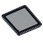
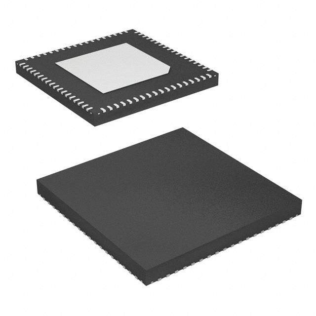
ICGOO电子元器件商城为您提供AD9484BCPZ-500由Analog设计生产,在icgoo商城现货销售,并且可以通过原厂、代理商等渠道进行代购。 AD9484BCPZ-500价格参考。AnalogAD9484BCPZ-500封装/规格:数据采集 - 模数转换器, 8 Bit Analog to Digital Converter 1 Input 1 Pipelined 56-LFCSP-VQ (8x8)。您可以下载AD9484BCPZ-500参考资料、Datasheet数据手册功能说明书,资料中有AD9484BCPZ-500 详细功能的应用电路图电压和使用方法及教程。
| 参数 | 数值 |
| 产品目录 | 集成电路 (IC)半导体 |
| 描述 | IC ADC 8BIT 500MSPS 56LFCSP模数转换器 - ADC 8-Bit 500 MSPS 1.8V |
| DevelopmentKit | AD9484-500EBZ |
| 产品分类 | |
| 品牌 | Analog Devices Inc |
| 产品手册 | |
| 产品图片 |
|
| rohs | 符合RoHS无铅 / 符合限制有害物质指令(RoHS)规范要求 |
| 产品系列 | 数据转换器IC,模数转换器 - ADC,Analog Devices AD9484BCPZ-500- |
| 数据手册 | |
| 产品型号 | AD9484BCPZ-500 |
| 产品种类 | 模数转换器 - ADC |
| 位数 | 8 |
| 供应商器件封装 | 56-LFCSP-VQ(8x8) |
| 信噪比 | 47 dB |
| 其它名称 | AD9484BCPZ500 |
| 分辨率 | 8 bit |
| 包装 | 托盘 |
| 商标 | Analog Devices |
| 安装类型 | 表面贴装 |
| 安装风格 | SMD/SMT |
| 封装 | Tray |
| 封装/外壳 | 56-VFQFN 裸露焊盘,CSP |
| 封装/箱体 | LFCSP-56 |
| 工作温度 | -40°C ~ 85°C |
| 工作电源电压 | 1.8 V |
| 工厂包装数量 | 260 |
| 接口类型 | LVDS |
| 数据接口 | SPI |
| 最大功率耗散 | 670 mW |
| 最大工作温度 | + 85 C |
| 最小工作温度 | - 40 C |
| 标准包装 | 1 |
| 特性 | - |
| 电压参考 | Internal, External |
| 电压源 | 模拟和数字 |
| 系列 | AD9484 |
| 结构 | Pipeline |
| 转换器数 | 1 |
| 转换器数量 | 1 |
| 转换速率 | 500 MS/s |
| 输入数和类型 | 1 个差分,双极 |
| 输入类型 | Differential |
| 通道数量 | 1 Channel |
| 采样率(每秒) | 500M |


- 商务部:美国ITC正式对集成电路等产品启动337调查
- 曝三星4nm工艺存在良率问题 高通将骁龙8 Gen1或转产台积电
- 太阳诱电将投资9.5亿元在常州建新厂生产MLCC 预计2023年完工
- 英特尔发布欧洲新工厂建设计划 深化IDM 2.0 战略
- 台积电先进制程称霸业界 有大客户加持明年业绩稳了
- 达到5530亿美元!SIA预计今年全球半导体销售额将创下新高
- 英特尔拟将自动驾驶子公司Mobileye上市 估值或超500亿美元
- 三星加码芯片和SET,合并消费电子和移动部门,撤换高东真等 CEO
- 三星电子宣布重大人事变动 还合并消费电子和移动部门
- 海关总署:前11个月进口集成电路产品价值2.52万亿元 增长14.8%


PDF Datasheet 数据手册内容提取
8-Bit, 500 MSPS, 1.8 V Analog-to-Digital Converter AD9484 FEATURES FUNCTIONAL BLOCK DIAGRAM SNR = 47 dBFS at f up to 250 MHz at 500 MSPS VREF PWDN AGND AVDD IN ENOB of 7.5 bits at f up to 250 MHz at 500 MSPS (−1.0 dBFS) IN SFDR = 79 dBc at f up to 250 MHz at 500 MSPS (−1.0 dBFS) REFERENCE AD9484 IN Integrated input buffer CML DRVDD Excellent linearity VIN+ DRGND TRACK-AND-HOLD DNL = ±0.1 LSB typical VIN– ADC 8 OUTPUT 8 INL = ±0.1 LSB typical CORE STAGING D7± TO D0± LVDS LVDS at 500 MSPS (ANSI-644 levels) CLK+ CLOCK OR+ 1 GHz full power analog bandwidth CLK– MANAGEMENT OR– On-chip reference, no external decoupling required SERIAL PORT Low power dissipation DCO+ Pro6g7r0a mmWm aabt l5e0 (0n oMmSiPnSa—l) LinVpDuSt SvDolRt aoguet praunt ge SCLK/DFS SDIO CSB DCO– 09615-001 1.18 V p-p to 1.6 V p-p, 1.5 V p-p nominal Figure 1. 1.8 V analog and digital supply operation Selectable output data format (offset binary, twos complement, Gray code) Clock duty cycle stabilizer Integrated data capture clock APPLICATIONS Wireless and wired broadband communications Cable reverse path Communications test equipment Low cost digital oscilloscopes Satellite subsystems Power amplifier linearization GENERAL DESCRIPTION The AD9484 is an 8-bit, monolithic, sampling analog-to-digital Fabricated on an advanced BiCMOS process, the AD9484 is availa- converter (ADC) optimized for high performance, low power, ble in a 56-lead LFCSP, and is specified over the industrial and ease of use. The part operates at up to a 500 MSPS conver- temperature range (−40°C to +85°C). This product is protected sion rate and is optimized for outstanding dynamic performance by a U.S. patent. in wideband carrier and broadband systems. All necessary PRODUCT HIGHLIGHTS functions, including a sample-and-hold and voltage reference, 1. High Performance. are included on the chip to provide a complete signal conversion Maintains 47 dBFS SNR at 500 MSPS with a 250 MHz input. solution. The VREF pin can be used to monitor the internal 2. Ease of Use. reference or provide an external voltage reference (external LVDS output data and output clock signal allow interface reference mode must be enabled through the SPI port). to current FPGA technology. The on-chip reference and The ADC requires a 1.8 V analog voltage supply and a differen- sample-and-hold provide flexibility in system design. Use tial clock for full performance operation. The digital outputs are of a single 1.8 V supply simplifies system power supply design. LVDS (ANSI-644) compatible and support twos complement, 3. Serial Port Control. offset binary format, or Gray code. A data clock output is available Standard serial port interface supports various product for proper output data timing. functions, such as data formatting, power-down, gain adjust, and output test pattern generation. Rev. A Information furnished by Analog Devices is believed to be accurate and reliable. However, no responsibility is assumed by Analog Devices for its use, nor for any infringements of patents or other One Technology Way, P.O. Box 9106, Norwood, MA 02062-9106, U.S.A. rights of third parties that may result from its use. Specifications subject to change without notice. No license is granted by implication or otherwise under any patent or patent rights of Analog Devices. Tel: 781.329.4700 www.analog.com Trademarks and registered trademarks are the property of their respective owners. Fax: 781.461.3113 ©2011 Analog Devices, Inc. All rights reserved.
AD9484 TABLE OF CONTENTS Features .............................................................................................. 1 Theory of Operation ...................................................................... 14 Applications ....................................................................................... 1 Analog Input and Voltage Reference ....................................... 14 Functional Block Diagram .............................................................. 1 Clock Input Considerations ...................................................... 15 General Description ......................................................................... 1 Power Dissipation and Power-Down Mode ........................... 16 Product Highlights ........................................................................... 1 Digital Outputs ........................................................................... 16 Revision History ............................................................................... 2 Timing ......................................................................................... 17 Specifications ..................................................................................... 3 VREF ............................................................................................ 17 DC Specifications ......................................................................... 3 AD9484 Configuration Using the SPI ..................................... 18 AC Specifications .......................................................................... 4 Hardware Interface ..................................................................... 18 Digital Specifications ................................................................... 5 Configuration Without the SPI ................................................ 18 Switching Specifications .............................................................. 6 Memory Map .................................................................................. 20 Absolute Maximum Ratings ............................................................ 7 Reading the Memory Map Table .............................................. 20 Thermal Resistance ...................................................................... 7 Reserved Locations .................................................................... 20 ESD Caution .................................................................................. 7 Default Values ............................................................................. 20 Pin Configuration and Function Descriptions ............................. 8 Logic Levels ................................................................................. 20 Typical Performance Characteristics ........................................... 10 Outline Dimensions ....................................................................... 23 Equivalent Circuits ......................................................................... 13 Ordering Guide .......................................................................... 23 REVISION HISTORY 6/11—Rev. 0 to Rev. A Change to General Description Section ........................................ 1 Change to Aperture Time Parameter in Table 4 ........................... 6 Change to Figure 34 ....................................................................... 16 Changes to Register 17 and Register 18 in Table 12 .................. 20 3/11—Revision 0: Initial Version Rev. A | Page 2 of 24
AD9484 SPECIFICATIONS DC SPECIFICATIONS AVDD = 1.8 V, DRVDD = 1.8 V, T = −40°C, T = +85°C, f = −1.0 dBFS, full scale = 1.5 V, unless otherwise noted. MIN MAX IN Table 1. Parameter1 Temp Min Typ Max Unit RESOLUTION 8 Bits ACCURACY No Missing Codes Full Guaranteed Offset Error 25°C 0 mV Full −3.0 +3.0 mV Gain Error 25°C 1.0 % FS Full −5.0 +7.0 % FS Differential Nonlinearity (DNL) 25°C ±0.13 LSB Full −0.25 +0.25 LSB Integral Nonlinearity (INL) 25°C ±0.1 LSB Full −0.15 +0.15 LSB INTERNAL REFERENCE VREF Full 0.71 0.75 0.78 V TEMPERATURE DRIFT Offset Error Full 18 μV/°C Gain Error Full 0.07 %/°C ANALOG INPUTS (VIN+, VIN−) Differential Input Voltage Range2 Full 1.18 1.5 1.6 V p-p Input Common-Mode Voltage Full 1.7 V Input Resistance (Differential) Full 1 kΩ Input Capacitance (Differential) Full 1.3 pF POWER SUPPLY AVDD Full 1.75 1.8 1.9 V DRVDD Full 1.75 1.8 1.9 V Supply Currents I 3 Full 283 300 mA AVDD I 3/SDR Mode4 Full 89 100 mA DRVDD Power Dissipation SDR Mode4 Full 670 720 mW Standby Mode Full 40 50 mW Power-Down Mode Full 2.5 7 mW 1 See the AN-835 Application Note, Understanding High Speed ADC Testing and Evaluation, for a complete set of definitions and how these tests were completed. 2 The input range is programmable through the SPI, and the range specified reflects the nominal values of each setting. See the Memory Map section. 3 IAVDD and IDRVDD are measured with a −1 dBFS, 10.3 MHz sine input at a rated sample rate. 4 Single data rate mode; this is the default mode of the AD9484. Rev. A | Page 3 of 24
AD9484 AC SPECIFICATIONS AVDD = 1.8 V, DRVDD = 1.8 V, T = −40°C, T = +85°C, f = −1.0 dBFS, full scale = 1.5 V, unless otherwise noted. MIN MAX IN Table 2. Parameter1, 2 Temp Min Typ Max Unit SNR f = 30.3 MHz 25°C 47.0 dBFS IN f = 70.3 MHz 25°C 47.0 dBFS IN f = 100.3 MHz 25°C 47.0 dBFS IN Full 46.5 dBFS f = 250.3 MHz 25°C 47.0 dBFS IN f = 450.3 MHz 25°C 46.9 dBFS IN SINAD f = 30.3 MHz 25°C 47.0 dBFS IN f = 70.3 MHz 25°C 47.0 dBFS IN f = 100.3 MHz 25°C 47.0 dBFS IN Full 46.4 dBFS f = 250.3 MHz 25°C 47.0 dBFS IN f = 450.3 MHz 25°C 46.9 dBFS IN EFFECTIVE NUMBER OF BITS (ENOB) f = 30.3 MHz 25°C 7.5 Bits IN f = 70.3 MHz 25°C 7.5 Bits IN f = 100.3 MHz 25°C 7.5 Bits IN f = 250.3 MHz 25°C 7.5 Bits IN f = 450.3 MHz 25°C 7.5 Bits IN WORST HARMONIC (SECOND or THIRD) f = 30.3 MHz 25°C −87 dBc IN f = 70.3 MHz 25°C −86 dBc IN f = 100.3 MHz 25°C −87 dBc IN Full −75 dBc f = 250.3 MHz 25°C 83 dBc IN f = 450.3 MHz 25°C 70 dBc IN SFDR f = 30.3 MHz 25°C 82 dBc IN f = 70.3 MHz 25°C 81 dBc IN f = 100.3 MHz 25°C 82 dBc IN Full 75 dBc f = 250.3 MHz 25°C 79 dBc IN f = 450.3 MHz 25°C 70 dBc IN WORST OTHER HARMONIC (SFDR EXCLUDING SECOND and THIRD) f = 30.3 MHz 25°C −82 dBc IN f = 70.3 MHz 25°C −81 dBc IN f = 100.3 MHz 25°C −82 dBc IN Full −75 dBc f = 250.3 MHz 25°C 79 dBc IN f = 450.3 MHz 25°C 77 dBc IN TWO-TONE IMD f = 119.5 MHz, f = 122.5 MHz 25°C −77 dBc IN1 IN2 ANALOG INPUT BANDWIDTH Full Power 25°C 1 GHz 1 All ac specifications tested by driving CLK+ and CLK− differentially. 2 See the AN-835 Application Note, Understanding High Speed ADC Testing and Evaluation, for a complete set of definitions and how these tests were completed. Rev. A | Page 4 of 24
AD9484 DIGITAL SPECIFICATIONS AVDD = 1.8 V, DRVDD = 1.8 V, T = −40°C, T = +85°C, f = −1.0 dBFS, full scale = 1.5 V, unless otherwise noted. MIN MAX IN Table 3. Parameter1 Temp Min Typ Max Unit CLOCK INPUTS Logic Compliance Full CMOS/LVDS/LVPECL Internal Common-Mode Bias Full 0.9 V Differential Input Voltage High Level Input (V ) Full 0.2 1.8 V p-p IH Low Level Input (V ) Full −1.8 −0.2 V p-p IL High Level Input Current (I ) Full −10 +10 μA IH Low Level Input Current (I ) Full −10 +10 μA IL Input Resistance (Differential) Full 8 10 12 kΩ Input Capacitance Full 4 pF LOGIC INPUTS Logic 1 Voltage Full 0.8 × DRVDD V Logic 0 Voltage Full 0.2 × DRVDD V Logic 1 Input Current (SDIO, CSB) Full 0 μA Logic 0 Input Current (SDIO, CSB) Full −60 μA Logic 1 Input Current (SCLK, PDWN) Full 50 μA Logic 0 Input Current (SCLK, PDWN) Full 0 μA Input Capacitance Full 4 pF LOGIC OUTPUTS2 V Differential Output Voltage Full 247 454 mV OD V Output Offset Voltage Full 1.125 1.375 V OS Output Coding 1 See the AN-835 Application Note, Understanding High Speed ADC Testing and Evaluation, for a complete set of definitions and how these tests were completed. 2 LVDS RTERMINATION = 100 Ω. Rev. A | Page 5 of 24
AD9484 SWITCHING SPECIFICATIONS AVDD = 1.8 V, DRVDD = 1.8 V, T = −40°C, T = +85°C, f = −1.0 dBFS, full scale = 1.5 V, unless otherwise noted. MIN MAX IN Table 4. Parameter Temp Min Typ Max Unit Maximum Conversion Rate Full 500 MSPS Minimum Conversion Rate Full 50 MSPS CLK+ Pulse Width High (tCH)1 Full 0.9 11 ns CLK+ Pulse Width Low (tCL)1 Full 0.9 11 ns Output (LVDS—SDR)1 Data Propagation Delay (t ) Full 0.85 ns PD Rise Time (t) (20% to 80%) 25°C 0.15 ns R Fall Time (t) (20% to 80%) 25°C 0.15 ns F DCO Propagation Delay (t ) Full 0.6 ns CPD Data to DCO Skew (t ) Full −0.07 +0.07 ns SKEW Latency Full 15 Clock cycles Aperture Time (t ) 25°C 0.85 ns A Aperture Uncertainty (Jitter, t) 25°C 80 fs rms J 1 See Figure 2. Timing Diagram N – 1 tA N + 4 N + 5 N N + 3 VIN+, VIN– N + 1 N + 2 tCH tCL 1/fS CLK+ CLK– t CPD DCO+ DCO– t SKEW t PD Dx+ Dx– N – 15 N – 14 N – 13 N – 12 N – 11 09615-002 Figure 2. Timing Diagram Rev. A | Page 6 of 24
AD9484 ABSOLUTE MAXIMUM RATINGS Table 5. Stresses above those listed under Absolute Maximum Ratings Parameter Rating may cause permanent damage to the device. This is a stress Electrical rating only; functional operation of the device at these or any AVDD to AGND −0.3 V to +2.0 V other conditions above those indicated in the operational DRVDD to DRGND −0.3 V to +2.0 V section of this specification is not implied. Exposure to absolute maximum rating conditions for extended periods may affect AGND to DRGND −0.3 V to +0.3 V device reliability. AVDD to DRVDD −2.0 V to +2.0 V D0+/D0− through D7+/D7− −0.3 V to DRVDD + 0.2 V THERMAL RESISTANCE to DRGND The exposed paddle must be soldered to the ground plane for DCO+, DCO− to DRGND −0.3 V to DRVDD + 0.2 V the LFCSP package. Soldering the exposed paddle to the PCB OR+, OR− to DRGND −0.3 V to DRVDD + 0.2 V increases the reliability of the solder joints, maximizing the CLK+ to AGND −0.3 V to AVDD + 0.2 V thermal capability of the package. CLK− to AGND −0.3 V to AVDD + 0.2 V VIN+ to AGND −0.3 V to AVDD + 0.2 V Table 6. VIN− to AGND −0.3 V to AVDD + 0.2 V Package Type θ θ Unit JA JC SDIO/DCS to DRGND −0.3 V to DRVDD + 0.2 V 56-Lead LFCSP_VQ (CP-56-5) 23.7 1.7 °C/W PDWN to AGND −0.3 V to DRVDD + 0.2 V Typical θ and θ are specified for a 4-layer board in still air. CSB to AGND −0.3 V to DRVDD + 0.2 V JA JC Airflow increases heat dissipation, effectively reducing θ . In SCLK/DFS to AGND −0.3 V to DRVDD + 0.2 V JA addition, metal in direct contact with the package leads from CML to AGND −0.3 V to AVDD + 0.2 V metal traces, through holes, ground, and power planes reduces VREF to AGND −0.3 V to AVDD + 0.2 V the θ . Environmental JA Storage Temperature Range −65°C to +125°C Operating Temperature Range −40°C to +85°C ESD CAUTION Lead Temperature 300°C (Soldering, 10 sec) Junction Temperature 150°C Rev. A | Page 7 of 24
AD9484 PIN CONFIGURATION AND FUNCTION DESCRIPTIONS DD CCCCCC+O–ONGDVDD–K+KDD NNNNNNCCRRVLLV DDDDDDDDDDACCA 6555453525150594847464544434 DNC 1 PIN 1 42 AVDD DNC 2 INDICATOR 41 AVDD D0– 3 40 CML D0+ 4 39 AVDD D1– 5 38 AVDD D1+ 6 AD9484 37 AVDD DRVDD 7 36 VIN– DRGND 8 TOP VIEW 35 VIN+ D2– 9 (Not to Scale) 34 AVDD D2+ 10 33 AVDD D3– 11 32 AVDD D3+ 12 31 VREF D4– 13 PIN 0 (EXPOSED PADDLE) = AGND 30 AVDD D4+ 14 29 PWDN 5161718191021222324252627282 –5D+5D–6D+6D–7D+7D–RO+RODNGRDDVRODISSFD/KBSCCND DD L C S NOTES 1. DNC = DO NOT CONNECT. DO NOT CONNECTTO THIS PIN. 2. AGND AND DRGND SHOULD BE TIED TO A COMMON 3. QAT HUGEIER ETO XUGPNRODOS UPENLDAD PN PAELD.ADNLEE. MUST BE SOLDERED TO 09615-003 Figure 3. Pin Configuration Table 7. Pin Function Descriptions Pin No. Mnemonic Description 0 AGND1 Analog Ground. The exposed paddle must be soldered to a ground plane. 30, 32 to 34, 37 to 39, AVDD 1.8 V Analog Supply. 41 to 43, 46 7, 24, 47 DRVDD 1.8 V Digital Output Supply. 8, 23, 48 DRGND1 Digital Output Ground. 35 VIN+ Analog Input—True. 36 VIN− Analog Input—Complement. 40 CML Common-Mode Output. Enabled through the SPI, this pin provides a reference for the optimized internal bias voltage for VIN+/VIN−. 44 CLK+ Clock Input—True. 45 CLK− Clock Input—Complement. 31 VREF Voltage Reference Internal/Input/Output. Nominally 0.75 V. 1, 2, 28, 51 to 56 DNC Do Not Connect. Do not connect to this pin. This pin should be left floating. 25 SDIO Serial Port Interface (SPI) Data Input/Output. 26 SCLK/DFS Serial Port Interface Clock (Serial Port Mode)/Data Format Select (External Pin Mode). 27 CSB Serial Port Chip Select (Active Low). 29 PWDN Chip Power-Down. 49 DCO− Data Clock Output—Complement. 50 DCO+ Data Clock Output—True. 3 D0− D0 Complement Output (LSB). 4 D0+ D0 True Output (LSB). 5 D1− D1 Complement Output. 6 D1+ D1 True Output. 9 D2− D2 Complement Output. 10 D2+ D2 True Output. 11 D3− D3 Complement Output. 12 D3+ D3 True Output. 13 D4− D4 Complement Output. Rev. A | Page 8 of 24
AD9484 Pin No. Mnemonic Description 14 D4+ D4 True Output. 15 D5− D5 Complement Output. 16 D5+ D5 True Output. 17 D6− D6 Complement Output. 18 D6+ D6 True Output. 19 D7− D7 Complement Output (MSB). 20 D7+ D7 True Output (MSB). 21 OR− Overrange Complement Output. 22 OR+ Overrange True Output. 1 Tie AGND and DRGND to a common quiet ground plane. Rev. A | Page 9 of 24
AD9484 TYPICAL PERFORMANCE CHARACTERISTICS AVDD = 1.8 V, DRVDD = 1.8 V, rated sample rate, T = 25°C, 1.5 V p-p differential input, AIN = −1 dBFS, unless otherwise noted. A 0 0 500MSPS 500MSPS –10 30.3MHzAT –1.0dBFS –10 270.3MHzAT –1.0dBFS SNR:46.0dB SNR:46.0dB –20 ENOB:7.5BITS –20 ENOB:7.5BITS SFDR: 82dBc SFDR: 79dBc –30 –30 S) S) F F dB –40 dB –40 E ( E ( D –50 D –50 U U T T LI –60 LI –60 P P M M A –70 A –70 –80 –80 –90 –90 –1000 20 40 60 80FR1E00QU1E2N0CY14 (0MH1z6)0 180 200 220 240 09615-106 –1000 20 40 60 80FR1E00QU1E2N0CY14 (0MH1z6)0 180 200 220 240 09615-109 Figure 4. 64k Point Single-Tone FFT; 500 MSPS, 30.3 MHz Figure 7. 64k Point Single-Tone FFT; 500 MSPS, 270.3 MHz 0 0 500MSPS 500MSPS –10 100.3MHzAT –1.0dBFS –10 450.3MHzAT –1.0dBFS SNR:46.0dB SNR:45.9dB –20 ESFNDORB:: 873.5dBBcITS –20 ENOB:7.5BITS SFDR: 70dBc –30 –30 S) S) F F dB –40 dB –40 E ( E ( D –50 D –50 U U T T LI –60 LI –60 P P M M A –70 A –70 –80 –80 –90 –90 –1000 20 40 60 80FR1E00QU1E2N0CY14 (0MH1z6)0 180 200 220 240 09615-107 –1000 20 40 60 80FR1E00QU1E2N0CY14 (0MH1z6)0 180 200 220 240 09615-110 Figure 5. 64k Point Single-Tone FFT; 500 MSPS, 100.3 MHz Figure 8. 64k Point Single-Tone FFT; 500 MSPS, 450.3 MHz 0 85 SFDR(dBc),TA=+25°C –10 500MSPS 80 140.3MHzAT –1.0dBFS –20 SNR:46.0dB ENOB:7.5BITS 75 –30 SFDR: 82dBc SFDR(dBc),TA=+85°C S) 70 AMPLITUDE (dBF ––––64750000 SNR/SFDR (dB) 566505 SSNNRR((ddBBFFSS)),,TTAA==+–4205°°CCSFDR(dBc),TA=–40°C –80 50 SNR(dBFS),TA=+85°C –90 45 –1000 20 40 60 80FR1E00QU1E2N0CY14 (0MH1z6)0 180 200 220 240 09615-108 400 100ANALOG 2IN00PUTFREQ3U0E0CY(MHz)400 500 09615-111 Figure 6. 64k Point Single-Tone FFT; 500 MSPS, 140.3 MHz Figure 9. Single-Tone SNR/SFDR vs. Input Frequency (fIN) and Temperature; 500 MSPS Rev. A | Page 10 of 24
AD9484 85 0.10 SFDR (dBc), 30.3MHz 80 0.08 75 SFDR (dBc), 100.3MHz 0.06 0.04 70 B) R (d 65 SB) 0.02 NR/SFD 60 DNL (L–0.020 S 55 –0.04 SNR (dBFS), 30.3MHz 50 SNR (dBFS), 100.3MHz –0.06 45 –0.08 4050 100 150 200SAM25P0LE R30A0TE (3M5S0PS)400 450 500 550 09615-112 –0.100 64 OUTPU12T8 CODE 192 256 09615-115 Figure 10. SNR/SFDR vs. Sample Rate; 30.3 MHz, 100.3 MHz Figure 13. DNL, 500 MSPS 100 4.0 0.29 LSB rms 90 SFDR (dBFS) 3.5 80 SFDR (dBc) 3.0 70 M) B) S ( 2.5 FDR (d 5600 SNR (dBFS) OF HIT 2.0 S R SNR/ 40 MBE 1.5 U 30 N SNR (dB) 1.0 20 10 0.5 0–50 –45 –40 –35 A–3M0PLI–T2U5DE –(d20B) –15 –10 –5 0 09615-211 0 N – 3 N – 2 N – 1 BINNS N + 1 N + 2 N + 3 09615-116 Figure 11. SNR/SFDR vs. Input Amplitude; 500 MSPS,140.3 MHz Figure 14. Grounded Input Histogram, 500 MSPS 0.10 0 0.08 –10 500MSPS 119.5MHzAT –7.0dBFS 122.5MHzAT –7.0dBFS 0.06 –20 SFDR: 77dBc 0.04 –30 S) F L (LSB) 0.020 UDE (dB ––4500 N T I–0.02 LI –60 P M –0.04 A –70 –0.06 –80 –0.08 –90 –0.100 64 OUTPU12T8 CODE 192 256 09615-114 –1000 20 40 60 80FR1E00QU1E2N0CY14 (0MH1z6)0 180 200 220 240 09615-215 Figure 12. INL, 500 MSPS Figure 15. 64k Point, Two-Tone FFT; 500 MSPS, 119.2 MHz, 122.5 MHz Rev. A | Page 11 of 24
AD9484 100 80 IMD3 (dBFS) 90 75 80 70 SFDR (dBFS) SFDR (dBc) 70 65 B) dB) 60 R (d 60 DR ( 50 SFD 55 SF 40 NR/ 50 SFDR (dBc) S 30 45 SNR (dBFS) 20 40 10 35 0 30 –90 –80 –70 –60AMP–L5I0TUDE–4 (0dBFS–)30 –20 –10 0 09615-118 500 600 FR7E00QUENCY (8M0H0z) 900 1000 09615-121 Figure 16. Two-Tone SFDR vs. Input Amplitude; 500 MSPS, Figure 19. SNR/SFDR at 500 MSPS; AIN Sweep at −1.0 dBFS 119.5 MHz, 122.5 MHz 90 SFDR (dBc) 80 70 B) d R ( FD 60 S R/ N S 50 SNR (dBFS) 40 30 1.5 1.6 1.7 VCM (V)1.8 1.9 2.0 09615-119 Figure 17. SNR/SFDR vs. Common-Mode Voltage; 500 MSPS, AIN = 140.3 MHz 350 800 700 300 TOTAL POWER 600 250 mA) IAVDD 500 W) NT ( 200 400 R (m E E R W CUR 300 PO 150 200 100 IDRVDD 100 50 0 5075100125150175200SA225M250PLE275 R300AT325E (M350S375PS)400425450475500525550 09615-120 Figure 18. Current and Power vs. Sample Rate, AIN = 30.3 MHz Rev. A | Page 12 of 24
AD9484 EQUIVALENT CIRCUITS AVDD DRVDD AVDD AVDD 0.9V DRVDD 15kΩ 15kΩ CLK+ CLK– 30kΩ DRVDD 350Ω CSB 09615-006 09615-009 Figure 20. Clock Inputs Figure 24. Equivalent CSB Input Circuit VBOOST AVDD DRVDD CML V+ V– Dx– Dx+ AVDD V– V+ VIN+ AIN+ 09615-010 500Ω DC Figure 25. LVDS Outputs (Dx+, Dx−, OR+, OR−, DCO+, DCO−) AVDD 500Ω SPI CONTROLLED AVDD VIN+ AIN– (00) 20kΩ (01) 09615-007 VREF Figure 21. Analog Input DC Equivalent Circuit (VCML = ~1.7 V) (10) NOT USED DRVDD (11) SPI CTRL VREF SELECT 00 = INTERNAL VREF 350Ω DRVDD Figure 26. Equivalent VR011E110F = ==I n NEIMpOXuPPTtOO /URORSTuTE tVDVpRRuEEFtF Circuit 09615-011 SCLK/DFS 30kΩ 09615-008 DRVDD DRVDD Figure 22. Equivalent SCLK/DFS, PDWN Input Circuit 30kΩ 350Ω VIN+ SDIO 1.3pF 1kΩ VIN– 09615-025 CTRL09615-012 Figure 23. Analog Input AC EquivalentCircuit Figure 27. Equivalent SDIO Input Circuit Rev. A | Page 13 of 24
AD9484 THEORY OF OPERATION The AD9484 architecture consists of a front-end sample-and- Differential Input Configurations hold amplifier (SHA) followed by a pipelined switched capacitor Optimum performance is achieved while driving the AD9484 ADC. The quantized outputs from each stage are combined into in a differential input configuration. For baseband applications, a final 8-bit result in the digital correction logic. The pipelined the AD8138 differential driver provides excellent performance architecture permits the first stage to operate on a new input and a flexible interface to the ADC. The output common-mode sample, whereas the remaining stages operate on preceding voltage of the AD8138 is easily set to AVDD/2 + 0.5 V, and the samples. Sampling occurs on the rising edge of the clock. driver can be configured in a Sallen-Key filter topology to pro- Each stage of the pipeline, excluding the last, consists of a low vide band limiting of the input signal. resolution flash ADC connected to a switched capacitor DAC and interstage residue amplifier (MDAC). The residue amplifier 1V p-p 49.9Ω magnifies the difference between the reconstructed DAC output 499Ω AVDD 33Ω and the flash input for the next stage in the pipeline. One bit of 499Ω VIN+ redundancy is used in each stage to facilitate digital correction AD8138 20pF AD9484 523Ω of flash errors. The last stage simply consists of a flash ADC. 0.1µF VIN– Tdch-ec oinuppulet ds tiang ed icfofenrteanintisa la o dri fsfienrgelnet-ieanl dSeHdA m tohdate .c Tanh eb eo uatcp-u otr 499Ω 33Ω CML 09615-013 staging block aligns the data, carries out the error correction, Figure 28. Differential Input Configuration Using the AD8138 and passes the data to the output buffers. The output buffers At input frequencies in the second Nyquist zone and above, the are powered from a separate supply, allowing adjustment of the performance of most amplifiers may not be adequate to achieve output voltage swing. During power-down, the output buffers the true performance of the AD9484. This is especially true in enter a high impedance state. IF undersampling applications where frequencies in the 70 MHz ANALOG INPUT AND VOLTAGE REFERENCE to 100 MHz range are being sampled. For these applications, differential transformer coupling is the recommended input The analog input to the AD9484 is a differential buffer. For best configuration. The signal characteristics must be considered dynamic performance, match the source impedances driving when selecting a transformer. Most RF transformers saturate at VIN+ and VIN− such that common-mode settling errors are frequencies below a few megahertz (MHz), and excessive signal symmetrical. The analog input is optimized to provide superior power can cause core saturation, which leads to distortion. wideband performance and requires that the analog inputs be In any configuration, the value of the shunt capacitor, C (see driven differentially. SNR and SINAD performance degrades Figure 30), is dependent on the input frequency and may need significantly if the analog input is driven with a single-ended to be reduced or removed. signal. A wideband transformer, such as Mini-Circuits® ADT1-1WT, 15Ω can provide the differential analog inputs for applications that VIN+ require a single-ended-to-differential conversion. Both analog 1.5V p-p 50Ω 2pF AD9484 inputs are self-biased by an on-chip reference to a nominal 1.7 V. VIN– Aneng aintitveer nreafl edriefnfecree nvotilatal gveosl ttahgaet rdeefefirneen cthe ec r1e.5at Ves pp-ops iftiixveed a snpda n 0.1µF 15Ω 09615-014 Figure 29. Differential Transformer—Coupled Configuration of the ADC core. This internal voltage reference can be adjusted by means of SPI control. See the AD9484 Configuration Using As an alternative to using a transformer-coupled input at frequen- the SPI section for more details. cies in the second Nyquist zone, the AD8352 differential driver can be used (see Figure 30). Rev. A | Page 14 of 24
AD9484 VCC 0.1µF 0.1µF 0Ω 16 8, 13 ANALOG INPUT 1 11 0.1µF R 2 VIN+ 200Ω CD RD RG AD8352 C AD9484 3 0.1µF 200Ω R 4 VIN– CML ANALOG INPUT 5 10 14 0.1µF 0Ω 0.1µF 0.1µF 09615-015 Figure 30. Differential Input Configuration Using the AD8352 AD9510/AD9511/ AD9512/AD9513/ AD9514/AD9515 0.1µF 0.1µF CLOCK INPUT CLK CLK+ ADC PECL DRIVER 100Ω AD9484 0.1µF 0.1µF CILNOPCUKT CLK CLK– 50Ω1 50Ω1 240Ω 240Ω 150Ω RESISTORS ARE OPTIONAL. 09615-017 Figure 31. Differential PECL Sample Clock AD9510/AD9511/ AD9512/AD9513/ AD9514/AD9515 0.1µF 0.1µF CLOCK INPUT CLK CLK+ ADC LVDS DRIVER 100Ω AD9484 0.1µF 0.1µF CILNOPCUKT CLK CLK– 50Ω1 50Ω1 150Ω RESISTORS ARE OPTIONAL. 09615-018 Figure 32. Differential LVDS Sample Clock CLOCK INPUT CONSIDERATIONS MINI-CIRCUITS For optimum performance, drive the AD9484 sample clock ADT1–1WT, 1:1Z 0.1µF 0.1µF inputs (CLK+ and CLK−) with a differential signal. This signal CLOCK XFMR CLK+ is typically ac-coupled into the CLK+ and CLK− pins via a INPUT 50Ω 100Ω ADC 0.1µF AD9484 transformer or capacitors. These pins are biased at ~0.9 V CLK– internally and require no additional bias. If the clock signal is dc-coupled, then the common-mode voltage should remain 0.1µF SHDCSIHOMOD2TE8T1SK2:Y 09615-016 within a range of 0.9 V. Figure 33. Transformer-Coupled Differential Clock Figure 33 shows one preferred method for clocking the AD9484. If a low jitter clock is available, another option is to ac couple a The low jitter clock source is converted from single-ended to differential PECL signal to the sample clock input pins, as differential using an RF transformer. The back-to-back Schottky shown in Figure 31. The AD9510/AD9511/AD9512/AD9513/ diodes across the secondary transformer limit clock excursions AD9514/AD9515 family of clock drivers offers excellent jitter into the AD9484 to approximately 0.8 V p-p differential. This performance. helps prevent the large voltage swings of the clock from feeding In some applications, it may be acceptable to drive the sample through to other portions of the AD9484 and preserves the fast clock inputs with a single-ended 1.8 V CMOS signal. In such rise and fall times of the signal, which are critical to low jitter applications, drive the CLK+ pin directly from a CMOS gate, performance. and bypass the CLK− pin to ground with a 0.1 μF capacitor in parallel with a 39 kΩ resistor (see Figure 34). Rev. A | Page 15 of 24
AD9484 130 VCC RMS CLOCK JITTER REQUIREMENT 120 0.1µF 1kΩ AD951x OP1T0IO0ΩNAL0.1µF CILNOPCUKT CMOS DRIVER CLK+ 110 50Ω1 1kΩ ADC 100 16 BITS AD9484 CLK– B) 90 14 BITS 150Ω RESISTOR IS OPTIONAL. 0.1µF 09615-024 SNR (d 7800 10 BITS 12 BITS Figure 34. Single-Ended 1.8 V CMOS Input Clock (Up to 200 MHz) 60 0.125ps Clock Duty Cycle Considerations 50 8 BITS 0.25ps 0.5ps Typical high speed ADCs use both clock edges to generate a 40 1.0ps 2.0ps vbaer sieetnys iotifv ien tteor cnlaolc tkim duintyg csiygcnlea.l sA. A5%s a t orelesuraltn, cteh eiss ec oAmDmCos nmlya y 301 ANALO1G0 INPUT FREQUENC10Y0 (MHz) 1000 09615-019 required on the clock duty cycle to maintain dynamic performance Figure 35. Ideal SNR vs. Input Frequency and Jitter characteristics. The AD9484 contains a duty cycle stabilizer (DCS) POWER DISSIPATION AND POWER-DOWN MODE that retimes the nonsampling edge, providing an internal clock signal with a nominal 50% duty cycle. This allows a wide range As shown in Figure 18, the power dissipated by the AD9484 is of clock input duty cycles without affecting the performance of proportional to its sample rate. The digital power dissipation the AD9484. When the DCS is on, noise and distortion perfor- does not vary much because it is determined primarily by the mance are nearly flat for a wide range of duty cycles. DRVDD supply and bias current of the LVDS output drivers. The duty cycle stabilizer uses a delay-locked loop (DLL) to By asserting PDWN (Pin 29) high, the AD9484 is placed in create the nonsampling edge. As a result, any changes to the standby mode or full power-down mode, as determined by the sampling frequency require approximately 15 clock cycles contents of Serial Port Register 08. Reasserting the PDWN pin to allow the DLL to acquire and lock to the new rate. low returns the AD9484 to its normal operational mode. Clock Jitter Considerations An additional standby mode is supported by means of varying the clock input. When the clock rate falls below 50 MHz, the High speed, high resolution ADCs are sensitive to the quality of the AD9484 assumes a standby state. In this case, the biasing network clock input. The degradation in SNR at a given input frequency and internal reference remain on, but digital circuitry is powered (f ) due only to aperture jitter (t) can be calculated by A J down. Upon reactivating the clock, the AD9484 resumes normal SNR Degradation = 20 × log (1/2 × π × f × t) 10 A J operation after allowing for the pipeline latency. In this equation, the rms aperture jitter represents the root mean DIGITAL OUTPUTS square of all jitter sources, including the clock input, analog input Digital Outputs and Timing signal, and ADC aperture jitter specifications. IF undersampling applications are particularly sensitive to jitter (see Figure 35). The AD9484 differential outputs conform to the ANSI-644 LVDS standard on default power-up. This can be changed to a Treat the clock input as an analog signal in cases where aperture low power, reduced signal option similar to the IEEE 1596.3 jitter may affect the dynamic range of the AD9484. Separate the standard using the SPI. This LVDS standard can further reduce power supplies for clock drivers from the ADC output driver the overall power dissipation of the device, which reduces the supplies to avoid modulating the clock signal with digital noise. power by ~39 mW. See the Memory Map section for more infor- Low jitter, crystal-controlled oscillators make the best clock mation. The LVDS driver current is derived on chip and sets sources. If the clock is generated from another type of source the output current at each output equal to a nominal 3.5 mA. (by gating, dividing, or other methods), it should be retimed by A 100 Ω differential termination resistor placed at the LVDS the original clock at the last step. receiver inputs results in a nominal 350 mV swing at the receiver. Refer to the AN-501 Application Note and the AN-756 The AD9484 LVDS outputs facilitate interfacing with LVDS Application Note for more in-depth information about jitter receivers in custom ASICs and FPGAs that have LVDS capability performance as it relates to ADCs (visit www.analog.com). for superior switching performance in noisy environments. Single point-to-point net topologies are recommended with a 100 Ω termination resistor placed as close to the receiver as possible. No far-end receiver termination or poor differential trace routing may result in timing errors. It is recommended that the trace length be no longer than 24 inches and that the Rev. A | Page 16 of 24
AD9484 differential output traces be kept close together and at equal Output Data Rate and Pinout Configuration lengths. The output data of the AD9484 can be configured to drive An example of the LVDS output using the ANSI standard (default) 12 pairs of LVDS outputs at the same rate as the input clock data eye and a time interval error (TIE) jitter histogram with signal (SDR mode). trace lengths less than 24 inches on regular FR-4 material is Out-of-Range (OR) shown in Figure 36. Figure 37 shows an example of when the An out-of-range condition exists when the analog input voltage trace lengths exceed 24 inches on regular FR-4 material. Notice is beyond the input range of the ADC. OR+ and OR− (OR±) that the TIE jitter histogram reflects the decrease of the data eye are digital outputs that are updated along with the data output opening as the edge deviates from the ideal position. It is up to corresponding to the particular sampled input voltage. Thus, the user to determine if the waveforms meet the timing budget OR± has the same pipeline latency as the digital data. OR± is of the design when the trace lengths exceed 24 inches. low when the analog input voltage is within the analog input 14 range and high when the analog input voltage exceeds the input 500 range, as shown in Figure 38. OR± remains high until the analog 12 400 V) s) input returns to within the input range and another conversion GE (m 230000 M (Hit10 is completed. By logically AND’ing OR± with the MSB and its A A complement, overrange high or underrange low conditions can OLT 100 OGR 8 be detected. RAM: V–1000 R HIST 6 OR± DATA OUTPUTS +FS – 1 LSB EYE DIAG––320000 TIE JITTE 4 100 111111111111 111111111110 OR± –FS + 1/2 LSB –400 2 –500 0 0000 0001 0 0000 0000 0 1 0000 0000 Figure 3–63. Da–2ta E–y1TeI MfoE0r (LnVsD)1S O2utpu3ts in AN–S4I0 Mod–e2 0wTitIMh ET0 r(apcse) L2e0ngth4s0 Le09615-020s s –FS – 1/–2F LSSB +FS – 1/+2F LSSB 09615-022 Than 24 Inches on Standard FR-4 Figure 38. OR± Relation to Input Voltage and Output Data 600 12 TIMING The AD9484 provides latched data outputs with a pipeline delay 400 10 GE (mV) 200 M(Hits) 8 odfe l1a5y c(ltoPDc)k a cfytecrle tsh. eD raistain ogu etdpguets o afr teh aev caliolacbkl es iognnea lp. ropagation A A RAM: VOLT 0 RHISTOGR 6 Moennit nsth icmeamniz edto et ghrreea dldeuenc getht ther aodnfy sntiheaenm tosiuc w tppiteuhrtfi ondr atmthaea l niAncDees 9o a4fn 8tdh4 e.l oTcaohdnessv epe rltatrecaren.d si - G E EYE DIA–200 TIEJITT 4 Tfohre c AapDtu9r4i8n4g athlseo d partoav iind easn a e dxtaetran calol rcekg oisutetpr.u Tt h(De CdaOta) oinuttepnudtes d –400 2 are valid on the rising edge of DCO. The lowest conversion rate of the AD9484 is 50 MSPS. At clock –600 0 –3 –2 –1TIME0(ns)1 2 3 –100 TIME0(ps) 100 09615-021 VraRteEs Fbe low 1 MSPS, the AD9484 assumes the standby mode. Figure 37. Data Eye for LVDS Outputs in ANSI Mode with Trace Lengths Greater Than 24 Inches on Standard FR-4 The AD9484 VREF pin (Pin 31) allows the user to monitor the on-board voltage reference, or provide an external reference The format of the output data is offset binary by default. An (requires configuration through the SPI). The three optional example of the output coding format can be found in Table 11. settings are internal V (pin is connected to 20 kΩ to ground), If it is desired to change the output data format to twos comple- REF export V , and import V . Do not attach a bypass capacitor ment, see the AD9484 Configuration Using the SPI section. REF REF to this pin. VREF is internally compensated and additional An output clock signal is provided to assist in capturing data loading may impact performance. from the AD9484. The DCO is used to clock the output data and is equal to the sampling clock (CLK) rate. In single data rate mode (SDR), data is clocked out of the AD9484 and must be captured on the rising edge of the DCO. See the timing diagram shown in Figure 2 for more information. Rev. A | Page 17 of 24
AD9484 AD9484 CONFIGURATION USING THE SPI command. This allows the serial data input/output (SDIO) pin to change direction from an input to an output. The AD9484 SPI allows the user to configure the converter for specific functions or operations through a structured register Data can be sent in MSB or in LSB first mode. MSB first is space inside the ADC. This gives the user added flexibility to default on power-up and can be changed by changing the customize device operation depending on the application. configuration register. For more information about this feature Addresses are accessed (programmed or readback) serially in and others, see the AN-877 Application Note, Interfacing to 1-byte words. Each byte can be further divided into fields, High Speed ADCs via SPI at www.analog.com. which are documented in the Memory Map section. HARDWARE INTERFACE There are three pins that define the serial port interface (SPI) to The pins described in Table 8 comprise the physical interface this particular ADC. They are the SCLK/DFS, SDIO and CSB between the programming device of the user and the serial port pins. The SCLK/DFS (serial clock) is used to synchronize the of the AD9484. The SCLK pin and the CSB pin function as read and write data presented the ADC. The SDIO (serial data inputs when using the SPI interface. The SDIO pin is bidirec- input/output) is a dual-purpose pin that allows data to be sent tional, functioning as an input during the write phase and as an to and read from the internal ADC memory map registers. The output during readback. CSB is an active low control that enables or disables the read This interface is flexible enough to be controlled by either and write cycles (see Table 8). PROMs or PIC® microcontrollers as well. This provides the user Table 8. Serial Port Pins with an alternate method to program the ADC other than a SPI Mnemonic Function controller. SCLK SCLK (serial clock) is the serial shift clock in. If the user chooses not to use the SPI interface, some pins serve SCLK is used to synchronize serial interface a dual function and are associated with a specific function when reads and writes. strapped externally to AVDD or ground during device power- SDIO SDIO (serial data input/output) is a dual-purpose on. The Configuration Without the SPI section describes the pin. The typical role for this pin is an input and output depending on the instruction being sent strappable functions supported on the AD9484. and the relative position in the timing frame. CONFIGURATION WITHOUT THE SPI CSB CSB (chip select) is an active low control that gates the read and write cycles. In applications that do not interface to the SPI control registers, the SCLK/DFS pin can alternately serve as a standalone CMOS- The falling edge of the CSB, in conjunction with the rising edge compatible control pin. Connect the CSB pin to AVDD, which of the SCLK, determines the start of the framing. An example of disables the serial port interface. the serial timing and its definitions can be found in Figure 39 and Table 10. Table 9. Mode Selection During an instruction phase, a 16-bit instruction is transmitted. External Data then follows the instruction phase and is determined by Mnemonic Voltage Configuration the W0 and W1 bits, which is one or more bytes of data. All SCLK/DFS AVDD Twos complement enabled data is composed of 8-bit words. The first bit of each individual AGND Offset binary enabled byte of serial data indicates whether this is a read or write tDS tHIGH tCLK tH tS tDH t LOW CSB SCLK DON’T CARE DON’T CARE SDIO DON’T CARE R/W W1 W0 A12 A11 A10 A9 A8 A7 D5 D4 D3 D2 D1 D0 DON’T CARE 09615-023 Figure 39. Serial Port Interface Timing Diagram Rev. A | Page 18 of 24
AD9484 Table 10. Serial Timing Definitions Parameter Minimum (ns) Description t 5 Setup time between the data and the rising edge of SCLK DS t 2 Hold time between the data and the rising edge of SCLK DH t 40 Period of the clock CLK t 5 Setup time between CSB and SCLK S t 2 Hold time between CSB and SCLK H t 16 Minimum period that SCLK should be in a logic high state HIGH t 16 Minimum period that SCLK should be in a logic low state LOW t 1 Minimum time for the SDIO pin to switch from an input to an output relative to the SCLK falling EN_SDIO edge (not shown in Figure 39) t 5 Minimum time for the SDIO pin to switch from an output to an input relative to the SCLK rising DIS_SDIO edge (not shown in Figure 39) Table 11. Output Data Format Input (V) Condition (V) Offset Binary Output Mode, D7± to D0± Twos Complement Mode, D7± to D0± OR± VIN+ − VIN− < −0.75 − 0.5 LSB 0000 0000 1000 0000 1 VIN+ − VIN− = −0.75 0000 0000 1000 0000 0 VIN+ − VIN− = 0 1000 0000 0000 0000 0 VIN+ − VIN− = 0.75 1111 1111 0111 1111 0 VIN+ − VIN− > 0.75 + 0.5 LSB 1111 1111 0111 1111 1 Rev. A | Page 19 of 24
AD9484 MEMORY MAP READING THE MEMORY MAP TABLE RESERVED LOCATIONS Each row in the memory map table (see Table 12) has eight Undefined memory locations should not be written to other address locations. The memory map is roughly divided into than with the default values suggested in this data sheet. Addresses three sections: chip configuration register map (Address 0x00 to that have values marked as 0 should be considered reserved and Address 0x02), transfer register map (Address 0xFF), and ADC have a 0 written into their registers during power-up. functions register map (Address 0x08 to Address 0x2A). DEFAULT VALUES The Addr. (Hex) column of the memory map indicates the register Coming out of reset, critical registers are preloaded with default address in hexadecimal, and the Default Value (Hex) column values. These values are indicated in Table 12. Other registers shows the default hexadecimal value that is already written into do not have default values and retain the previous value when the register. The Bit 7 (MSB) column is the start of the default exiting reset. hexadecimal value given. For example, Hexadecimal Address LOGIC LEVELS 0x2A, OVR_CONFIG, has a hexadecimal default value of 0x01. This means Bit 7 = 0, Bit 6 = 0, Bit 5 = 0, Bit 4 = 0, Bit 3 = 0, An explanation of various registers follows: “Bit is set” is Bit 2 = 0, Bit 1 = 0, and Bit 0 = 1, or 0000 0001 in binary. The synonymous with “bit is set to Logic 1” or “writing Logic 1 for default value enables the OR± output. Overwriting this default so the bit.” Similarly, “clear a bit” is synonymous with “bit is set to that Bit 0 = 0 disables the OR± output. For more information on Logic 0” or “writing Logic 0 for the bit.” this and other functions, consult the AN-877 Application Note, Interfacing to High-Speed ADCs via SPI® user manual at www.analog.com. Table 12. Memory Map Register Default Addr. Bit 7 Bit 0 Value Default Notes/ (Hex) Register Name (MSB) Bit 6 Bit 5 Bit 4 Bit 3 Bit 2 Bit 1 (LSB) (Hex) Comments Chip Configuration Registers 00 CHIP_PORT_CONFIG 0 LSB Soft 1 1 Soft LSB 0 0x18 The nibbles first reset reset first should be mirrored by the user so that LSB or MSB first mode registers correctly, regardless of shift mode. 01 CHIP_ID 8-bit chip ID, Bits[7:0] = 0x6C Read Default is a only unique chip ID, different for each device. This is a read- only register. 02 CHIP_GRADE 0 0 0 Speed grade: X1 X 1 X1 Read Child ID used to X 00 = 500 MSPS only differentiate graded devices. Transfer Register FF DEVICE_UPDATE 0 0 0 0 0 0 0 SW 0x00 Synchronously transfer transfers data from the master shift register to the slave. ADC Functions Registers 08 Modes 0 0 PDWN: 0 0 Internal power-down mode: 0x00 Determines 0 = full 000 = normal (power-up, various generic (default) default) modes of chip 1 = 001 = full power-down operation. standby 010 = standby 011 = normal (power-up) Note that external PDWN pin overrides this setting Rev. A | Page 20 of 24
AD9484 Default Addr. Bit 7 Bit 0 Value Default Notes/ (Hex) Register Name (MSB) Bit 6 Bit 5 Bit 4 Bit 3 Bit 2 Bit 1 (LSB) (Hex) Comments 10 Offset 8-bit device offset adjustment [7:0] 0x00 Device offset 0111 111 = +127 codes trim: codes are 0000 0000 = 0 codes relative to the 1000 0000 = −128 codes output resolution. 0D TEST_IO (For user-defined Reset Reset Output test mode: 0x00 When set, the mode only, set PN23 PN9 0000 = off (default) test data is Bits[3:0] = 1000) gen: gen: 0001 = midscale short placed on the 00 = Pattern 1 only 1 = on 1 = on 0010 = +FS short output pins in 01 = toggle P1/P2 0 = off 0 = off 0011 = −FS short place of normal 10 = toggle (default) (default) 0100 = checker board output data. P1/0000 0101 = PN23 sequence Set pattern 11 = toggle P1/P2/ 0110 = PN9 values: 0000 0111 = one/zero word toggle P1 = Reg 0x19, 1000 = user defined Reg 0x1A 1001 = unused P2 = Reg 0x1B, 1010 = unused Reg 0x1C 1011 = unused 1100 = unused (Format determined by OUTPUT_MODE) 0F AIN_CONFIG 0 0 0 0 0 Analog 0 0 0x00 input disable: 1 = on 0 = off (default) 14 OUTPUT_MODE 0 0 0 Output 0 Output Data format select: 0x00 0 enable: invert: 00 = offset binary 0 = 1 = on (default) enable 0 = off 01 = twos (default) (default) complement 1 = 10 = Gray code disable 15 OUTPUT_ADJUST 0 0 0 0 LVDS LVDS fine adjust: 0x00 0 course 001 = 3.50 mA adjust: 010 = 3.25 mA 0 = 011 = 3.00 mA 3.5 mA 100 = 2.75 mA (default) 101 = 2.50 mA 1 = 110 = 2.25 mA 2.0 mA 111 = 2.00 mA 16 OUTPUT_PHASE Output 0 0 0 0 0 0 0 0x00 clock polarity 1 = inverted 0 = normal (default) 17 FLEX_OUTPUT_DELAY 0 0 0 0 Output clock delay: 0x00 Shown as 0000 = 0 fractional value 0001 = −1/10 of sampling 0010 = −2/10 clock period 0011 = −3/10 that is 0100 = reserved subtracted or added to initial 0101 = +5/10 0110 = +4/10 tSKEW, see Figure 2. 0111 = +3/10 1000 = +2/10 1001 = +1/10 Rev. A | Page 21 of 24
AD9484 Default Addr. Bit 7 Bit 0 Value Default Notes/ (Hex) Register Name (MSB) Bit 6 Bit 5 Bit 4 Bit 3 Bit 2 Bit 1 (LSB) (Hex) Comments 18 FLEX_VREF VREF select 0 Input voltage range setting: 0x00 00 = internal VREF 11100 = 1.60 (20 kΩ pull-down) 11101 = 1.58 01 = import VREF 11110 = 1.55 (0.59 V to 0.8 V on 11111 = 1.52 VREF pin) 00000 = 1.50 00001 = 1.47 10 = export VREF 00010 = 1.44 (from internal 00011 = 1.42 reference) 00100 = 1.39 11 = not used 00101 = 1.36 00110 = 1.34 00111 = 1.31 01000 = 1.28 01001 = 1.26 01010 = 1.23 01011= 1.20 01011= 1.18 19 USER_PATT1_LSB 0x00 User-defined B7 B6 B5 B4 B3 B2 B1 B0 pattern, 1 LSB. 1A USER_PATT1_MSB 0x00 User-defined B7 B6 B5 B4 B3 B2 B1 B0 pattern, 1 MSB. 1B USER_PATT2_LSB 0x00 User-defined B7 B6 B5 B4 B3 B2 B1 B0 pattern, 2 LSBs. 1C USER_PATT2_MSB 0x00 User-defined B7 B6 B5 B4 B3 B2 B1 B0 pattern, 2 MSBs. 2A OVR_CONFIG 0 0 0 0 0 0 0 OR± 0x01 enable: 1 = on (default) 0 = off 2C Input coupling 0 0 0 0 0 DC 0 0 0x00 Default is coupling ac coupling. enable 1 X = don’t care. Rev. A | Page 22 of 24
AD9484 OUTLINE DIMENSIONS 8.10 0.60MAX 0.30 8.00SQ 0.23 7.90 0.60 0.18 MAX PIN1 43 56 INDICATOR 42 1 PIN1 0.50 INDICATOR BSC 7.85 7.75SQ EXPOSED 5.25 PAD 7.65 5.10SQ 4.95 14 29 TOPVIEW 00..5400 28 BOTTOMVIEW 15 0.25MIN 0.30 6.50REF 1.00 12°MAX 0.80MAX 0.85 0.65TYP FORPROPERCONNECTIONOF 0.80 0.05MAX TTHHEEPEIXNPCOOSNEDFIGPAUDR,ARTEIOFNERANTOD 0.02NOM FUNCTIONDESCRIPTIONS COPLANARITY SECTIONOFTHISDATASHEET. SEATING 0.20REF 0.08 PLANE COMPLIANTTOJEDECSTANDARDSMO-220-VLLD-2 081809-B Figure 40. 56-Lead Lead Frame Chip Scale Package [LFCSP_VQ] 8 mm × 8 mm Body, Very Thin Quad (CP-56-5) Dimensions shown in millimeters ORDERING GUIDE Model1 Temperature Range Package Description Package Option AD9484BCPZ-500 −40°C to +85°C 56-Lead Lead Frame Chip Scale Package [LFCSP_VQ] CP-56-5 AD9484BCPZRL7-500 −40°C to +85°C 56-Lead Lead Frame Chip Scale Package [LFCSP_VQ] CP-56-5 AD9484-500EBZ Evaluation Board 1 Z = RoHS Compliant Part. Rev. A | Page 23 of 24
AD9484 NOTES ©2011 Analog Devices, Inc. All rights reserved. Trademarks and registered trademarks are the property of their respective owners. D09615-0-6/11(A) Rev. A | Page 24 of 24