 Datasheet下载
- 型号: AD9388ABSTZ-5P
- 制造商: Analog
- 库位|库存: xxxx|xxxx
- 要求:
| 数量阶梯 | 香港交货 | 国内含税 |
| +xxxx | $xxxx | ¥xxxx |
查看当月历史价格
查看今年历史价格
AD9388ABSTZ-5P产品简介:
ICGOO电子元器件商城为您提供AD9388ABSTZ-5P由Analog设计生产,在icgoo商城现货销售,并且可以通过原厂、代理商等渠道进行代购。 AD9388ABSTZ-5P价格参考。AnalogAD9388ABSTZ-5P封装/规格:线性 - 视频处理, 。您可以下载AD9388ABSTZ-5P参考资料、Datasheet数据手册功能说明书,资料中有AD9388ABSTZ-5P 详细功能的应用电路图电压和使用方法及教程。
| 参数 | 数值 |
| 产品目录 | 集成电路 (IC)半导体 |
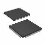
| 描述 | IC GRAPHIC DIGITIZER 144-LQFP视频 IC 10B Intg Mltiformat HDTV Video Decoder |
| 产品分类 | |
| 品牌 | Analog Devices |
| 产品手册 | |
| 产品图片 |
|
| rohs | 符合RoHS无铅 / 符合限制有害物质指令(RoHS)规范要求 |
| 产品系列 | 多媒体 IC,视频 IC,Analog Devices AD9388ABSTZ-5P- |
| 数据手册 | |
| 产品型号 | AD9388ABSTZ-5P |
| 产品种类 | 视频 IC |
| 供应商器件封装 | 144-LQFP(20x20) |
| 分辨率 | 10 bit |
| 包装 | 托盘 |
| 商标 | Analog Devices |
| 安装类型 | 表面贴装 |
| 封装 | Tray |
| 封装/外壳 | 144-LQFP |
| 封装/箱体 | LQFP |
| 工厂包装数量 | 60 |
| 应用 | HDTV |
| 最大工作温度 | + 85 C |
| 最小工作温度 | - 40 C |
| 标准包装 | 1 |
| 类型 | Digitizer with Dual Channel HDMI Receiver |
| 系列 | AD9388A |


- 商务部:美国ITC正式对集成电路等产品启动337调查
- 曝三星4nm工艺存在良率问题 高通将骁龙8 Gen1或转产台积电
- 太阳诱电将投资9.5亿元在常州建新厂生产MLCC 预计2023年完工
- 英特尔发布欧洲新工厂建设计划 深化IDM 2.0 战略
- 台积电先进制程称霸业界 有大客户加持明年业绩稳了
- 达到5530亿美元!SIA预计今年全球半导体销售额将创下新高
- 英特尔拟将自动驾驶子公司Mobileye上市 估值或超500亿美元
- 三星加码芯片和SET,合并消费电子和移动部门,撤换高东真等 CEO
- 三星电子宣布重大人事变动 还合并消费电子和移动部门
- 海关总署:前11个月进口集成电路产品价值2.52万亿元 增长14.8%


PDF Datasheet 数据手册内容提取
Dual HDMI Receiver, Multiformat HDTV Video Decoder, And RGB Graphics Digitizer AD9388A FEATURES GENERAL DESCRIPTION Dual HDMI 1.3 receiver The AD9388A is a high quality, single-chip graphics digitizer HDMI support with an integrated 2:1 multiplexed HDMI® receiver. Deep Color support The AD9388A contains one main component processor (CP) xvYCC enhanced colorimetry that processes YPrPb and RGB component formats, including Gamut metadata RGB graphics. The CP also processes the video signals from the 225 MHz HDMI receiver HDMI receiver. The AD9388A can keep the HDCP link between Repeater support an HDMI source and the selected HDMI port active in analog High-bandwidth digital content protection (HDCP 1.3) mode operation. This allows for fast switching between the S/PDIF (IEC60958-compatible) digital audio output analog and HDMI modes. Multichannel I2S audio output (up to 8 channels) Adaptive equalizer for cable lengths up to 30 meters The AD9388A supports the decoding of a component RGB or Internal EDID RAM YPrPb video signal into a digital YCrCb or RGB pixel output DVI 1.0 stream. The support for component video includes 525i, 625i, Multiformat decoder 525p, 625p, 720p, 1080i, 1080p, and 1250i standards, as well as Three 10-bit analog-to-digital converters (ADCs) many other HD and SMPTE standards. ADC sampling rates up to 170 MHz Graphics digitization is also supported by the AD9388A. The Mux with 12 analog input channels AD9388A is capable of digitizing RGB graphics signals from 525i-/625i-component SD support VGA to UXGA rates and converting them into a digital RGB 525p-/625p-component progressive scan support or YCrCb pixel output stream. 720p-/1080i-/1080p-component HDTV support The AD9388A incorporates a dual input HDMI-compatible Digitizes RGB graphics up to 1600 × 1200 at 60 Hz (UXGA) receiver that supports HDTV formats up to 1080p and display VBI data slicer (including teletext) resolutions up to UXGA (1600 × 1200 at 60 Hz). The reception Analog-to-HDMI fast switching of encrypted video is possible with the inclusion of HDCP. In General addition, the inclusion of adaptive equalization ensures robust Highly flexible output interface operation of the interface with cable lengths up to 30 meters. The STDI function support standard identification HDMI receiver has advanced audio functionality, such as a 2 any-to-any, 3 × 3 color-space conversion matrices mute controller that prevents audible extraneous noise in the Programmable interrupt request output pins audio output. APPLICATIONS Derivative parts of the AD9388A are available; AD9388ABSTZ-A5 Advanced TVs is composed of one analog and one digital input. To facilitate pro- PDP HDTVs fessional applications, where HDCP processing and decryption LCD TVs (HDTV ready) are not required, the AD9388ABSTZ-5P derivative is available. LCD/DLP® rear projection HDTVs This allows users who are not HDCP adopters to purchase the CRT HDTVs AD9388A (see the Ordering Guide section for details on these LCoS® HDTVs derivative parts). Audio/video receivers (AVRs) Fabricated in an advanced CMOS process, the AD9388A is LCD/DLP front projectors available in a space-saving, 144-lead, surface-mount, RoHS- HDTV STBs with PVR compliant, plastic LQFP and is specified over the −40°C to DVD recorders with progressive scan input support +85°C temperature range. Rev. F Information furnished by Analog Devices is believed to be accurate and reliable. However, no responsibility is assumed by Analog Devices for its use, nor for any infringements of patents or other One Technology Way, P.O. Box 9106, Norwood, MA 02062-9106, U.S.A. rights of third parties that may result from its use. Specifications subject to change without notice. No license is granted by implication or otherwise under any patent or patent rights of Analog Devices. Tel: 781.329.4700 www.analog.com Trademarks and registered trademarks are the property of their respective owners. Fax: 781.461.3113 ©2007–2010 Analog Devices, Inc. All rights reserved.
AD9388A TABLE OF CONTENTS Features..............................................................................................1 Component Processor Pixel Data Output Modes..................16 Applications.......................................................................................1 Component Video Processing..................................................16 General Description.........................................................................1 RGB Graphics Processing.........................................................16 Revision History...............................................................................2 General Features.........................................................................16 Functional Block Diagram..............................................................3 Theory of Operation......................................................................17 Specifications.....................................................................................4 Analog Front End.......................................................................17 Electrical Characteristics.............................................................4 HDMI Receiver...........................................................................17 Analog and HDMI Specifications..............................................6 Component Processor (CP)......................................................17 Data and I2C Timing Characteristics.........................................7 VBI Data Processor....................................................................17 Absolute Maximum Ratings............................................................9 Pixel Output Formatting................................................................18 Thermal Resistance......................................................................9 Register Map Architecture........................................................20 Package Thermal Performance...................................................9 Typical Connection Diagram...................................................21 ESD Caution..................................................................................9 Recommended External Loop Filter Components................22 Pin Configurations and Function Descriptions.........................10 AD9388A Evaluation Platform.....................................................23 Functional Overview......................................................................16 Outline Dimensions.......................................................................24 Analog Front End.......................................................................16 Ordering Guide..........................................................................24 HDMI Receiver...........................................................................16 REVISION HISTORY 10/10—Rev. E to Rev. F Added HDMI Registered Trademark............................................1 Changes to Features Section............................................................1 Changes to Ordering Guide..........................................................24 Added HDMI Paragraph...............................................................24 8/09—Rev. D to Rev. E Changes to Pin No. Order for AIN1 to AIN12 Pins (Table 6)........10 Changes to Ordering Guide...................................................................24 4/09—Rev. C to Rev. D Changes to Package Thermal Performance Section....................9 Changes to VBI Data Processor Section......................................17 1/09—Rev. B to Rev. C Changes to Static Performance Parameter and Power Requirements Parameter, Table 1..................................4 Changes to HDMI Specifications Parameter, Table 2..................6 Change to Maximum Junction Temperature (T ), Table 4.........9 J_MAX Changes to Package Thermal Performance Section....................9 Change to Figure 6.........................................................................13 Changes to AD9388A Evaluation Platform Section..................23 Changes to Table 13........................................................................23 Changes to Figure 11......................................................................23 Changes to Ordering Guide..........................................................24 7/08—Revision B: Initial Version Rev. F | Page 2 of 24
AD9388A FUNCTIONAL BLOCK DIAGRAM PIXELDATA P0 TOP9 P10 TOP19 P20 TOP29 INT1 HS/CS VS/FIELD DE/FIELD LLC SYNC_OUT/INT2 100-51960 10 10 10 RETTAMROF TUPTUO Y R AD9388A DIGITAL PROCESSING BLOCK COMPONENT PROCESSOR SYNC EXTRACT SYNC SOURCE ANDSTANDARDAV CODEPOLARITY DETECTIDENTIFICATIONINSERTION MACROVISION ANDCGMS DETECTION DIGITALOFFSETGAINPROG.FINEADDERCONTROLDELAYCLAMP ACTIVE PEAK ANDNOISE AND CALIBRATIONHSYNC DEPTH VBI DATA PROCESSORANCILLADATAANCILLARYVBIDATADECODERFORMATTER 2SILRCLKSCLKMCLKOUTSPDIF G N DATAPREPROCESSOR EMBEDDEDSYNC COLOR-SPACECONVERTER(A)(A)(B)(B)(C)(C) DECIMATIONANDDOWNSAMPLINGFILTERS AUDIOPROCESSI E MUX PACKET/NFOFRAMMEMORY A I G INTERFACE 10ADC0 10ADC1 10ADC2 HS/CS, VS CONTROL CONTROL AND DAT CONTROL FILTER 4:2:2 TO4:4:4CONVERSION PACKETPROCESSOR ANALO CLAMP INPUTCLAMPMATRIX CLAMP LLC GENERATION SYNC PROCESSING ANDCLOCK GENERATION CONTROL INTERFACE2IC HDMIDEXORECODEVS HS HDCPHDCPEEPROMENGINE MDA MCL D RGB YPrPb SOGSOYHS_IN/CS_INVS_IN SCLSDAALSB DATARECOVERYALIGNMENT EDID/REPEATERONTROLLER AALLCCDDSSSS____ABABCCCCDDDDDDDD C X U M R R E E MPL PLL MPL A A S S R R E E UALIZ MUX UALIZ Q Q E E RXA_0RXA_1RXA_2 RXA_CRXB_C RXB_0RXB_1RXB_2 Figure 1. Rev. F | Page 3 of 24
AD9388A SPECIFICATIONS ELECTRICAL CHARACTERISTICS AVDD = 1.71 V to 1.89 V, DVDD = 1.62 V to 1.98 V, DVDDIO = 2.97 V to 3.63 V, PVDD = 1.71 V to 1.89 V, TVDD = 3.135 V to 3.465 V, CVDD = 1.71 V to 1.89 V. Operating temperature range is −40°C to +85°C, unless otherwise noted. Table 1. Parameter1 Symbol Test Conditions Min Typ Max Unit 0F STATIC PERFORMANCE2 1F Resolution (Each ADC) N 10 Bits Integral Nonlinearity INL BSL at 27 MHz (@ a 10-bit level) –0.5/+2 LSB BSL at 54 MHz (@ a 10-bit level) –0.5/+2 LSB BSL at 74 MHz (@ a 10-bit level) –0.5/+1.5 LSB BSL at 110 MHz (@ a 10-bit level) –0.7/+2 LSB BSL at 170 MHz (@ an 8-bit level) –0.25/+0.5 LSB Differential Nonlinearity DNL At 27 MHz (@ a 10-bit level) –0.5/+0.5 LSB At 54 MHz (@ a 10-bit level) ±0.5 LSB At 74 MHz (@ a 10-bit level) ±0.5 LSB At 110 MHz (@ a 10-bit level) ±0.5 LSB At 170 MHz (@ an 8-bit level) –0.25/+0.2 LSB DIGITAL INPUTS Input High Voltage3 V 2 V 2F IH HS_IN, VS_IN low trigger mode 0.7 V Input Low Voltage3 V 0.8 V IL HS_IN, VS_IN low trigger mode 0.3 V Input Current IIN Pin 21 (AAARESETEEEAAA) –60 +60 μA All input pins other than Pin 21 –10 +10 μA Input Capacitance4 C 10 pF 3F IN DIGITAL OUTPUTS Output High Voltage5 V I = 0.4 mA 2.4 V 4F OH SOURCE Output Low Voltage5 V I = 3.2 mA 0.4 V OL SINK High Impedance Leakage Current I 10 μA LEAK Output Capacitance4 C 20 pF OUT POWER REQUIREMENTS4 Digital Core Power Supply DVDD 1.62 1.8 1.98 V Digital I/O Power Supply DVDDIO 2.97 3.3 3.63 V PLL Power Supply PVDD 1.71 1.8 1.89 V Analog Power Supply AVDD 1.71 1.8 1.89 V Terminator Power Supply TVDD 3.135 3.3 3.465 V Comparator Power Supply CVDD 1.71 1.8 1.89 V Digital Core Supply Current I Graphics RGB sampling @ 108 MHz6, 7 141 290 mA DVDD 5F YPrPb 1080p sampling @ 148.5 MHz6, 7 203 305 mA HDMI RGB sampling @ 165 MHz7, 8, 9 242 358 mA 7F 8F HDMI RGB sampling @ 225 MHz7, 8, 9 242 414 mA Digital I/O Supply Current I Graphics RGB sampling @ 108 MHz6, 7 17 80 mA DVDDIO YPrPb 1080p sampling @ 148.5 MHz6, 7 42 136 mA HDMI RGB sampling @ 165 MHz7, 8, 9 17 192 mA HDMI RGB sampling @ 225 MHz7, 8, 9 20 151 mA HDMI Comparators I Graphics RGB sampling @ 108 MHz6, 7 56 83 mA CVDD Rev. F | Page 4 of 24
AD9388A Parameter1 Symbol Test Conditions Min Typ Max Unit 0F TMDS PLL and Equalizer YPrPb 1080p sampling @ 148.5 MHz6, 7 56 83 mA Supply Current HDMI RGB sampling @ 165 MHz7, 8, 9 86 111 mA HDMI RGB sampling @ 225 MHz7, 8, 9 95 125 mA Analog Supply Current I Graphics RGB sampling @ 108 MHz6, 7 174 312 mA AVDD YPrPb 1080p sampling @ 148.5 MHz6, 7 180 318 mA HDMI RGB sampling @ 165 MHz7, 8, 9 0 2 mA HDMI RGB sampling @ 225 MHz7, 8, 9 0 2 mA Terminator Supply Current I Graphics RGB sampling @ 108 MHz6, 7 12 20 mA TVDD YPrPb 1080p sampling @ 148.5 MHz6, 7 12 20 mA HDMI RGB sampling @ 165 MHz7, 8, 9, 10 42 97 mA 9F HDMI RGB sampling @ 225 MHz7, 8, 9, 10 63 100 mA Audio and Video Supply Current I Graphics RGB sampling @ 108 MHz6, 7 14 22 mA PVDD YPrPb 1080p sampling @ 148.5 MHz6, 7 19 25 mA HDMI RGB sampling @ 165 MHz7, 8, 9 10 20 mA HDMI RGB sampling @ 225 MHz7, 8, 9 15 21 mA Power-Down Current I 11.6 mA PWRDN Power-Up Time t 25 ms PWRUP 1 The minimum/maximum specifications are guaranteed over the −40°C to +85°C temperature range (TMIN to TMAX). 2 All ADC linearity tests performed at input range of full scale − 12.5% and at zero scale + 12.5%. 3 Pin 1, Pin 105, Pin 106, and Pin 144 are 5 V tolerant. 4 Guaranteed by characterization. 5 VOH and VOL levels obtained using default drive strength value (0x15) in User Map Register 0xF4. 6 Current measurements for analog inputs were made with HDMI/analog simultaneous mode disabled (User Map Register 0xBA, Bit 7, programmed with Value 0) and no HDMI sources connected to the part. 7 Typical current measurements were taken with nominal voltage supply levels and an SMPTE bar video pattern input. Maximum current measurements were taken with maximum rating voltage supply levels and a MoiréX video pattern input. 8 Current measurements for HDMI inputs were made with a source connected to the active HDMI port and no source connected to the inactive HDMI port. 9 Audio stream is an uncompressed stereo audio sampling frequency of fS = 48 kHz and MCLKOUT = 256 fS. 10 The terminator supply current may vary with the HDMI source in use. Rev. F | Page 5 of 24
AD9388A ANALOG AND HDMI SPECIFICATIONS AVDD = 1.71 V to 1.89 V, DVDD = 1.62 V to 1.98 V, DVDDIO = 2.97 V to 3.63 V, PVDD = 1.71 V to 1.89 V, TVDD = 3.135 V to 3.465 V, CVDD = 1.71 V to 1.89 V. Operating temperature range is −40°C to +85°C, unless otherwise noted. Table 2. Parameter1, 2 Test Conditions Min Typ Max Unit 10F ANALOG Clamp Circuitry External Clamp Capacitor 0.1 μF Input Impedance (Except Pin 74) Clamps switched off 10 MΩ Input Impedance of Pin 74 20 kΩ CML 0.88 V ADC Full-Scale Level CML + 0.5 V ADC Zero-Scale Level CML − 0.5 V ADC Dynamic Range 1 V Clamp Level (When Locked) Component input (Y signal) CML − 0.120 V Component input (Pr signal) CML V Component input (Pb signal) CML V PC RGB input (R, G, B signals) CML − 0.120 V HDMI SPECIFICATIONS3 12F Intrapair (Positive-to-Negative) Differential Input 0.4 t bit Skew4, 5 13F 14F Channel-to-Channel Differential Input Skew5, 6 0.2 t + 1.78 ns 15F pixel 1 The minimum/maximum specifications are guaranteed over the −40°C to +85°C temperature range. 2 Guaranteed by characterization. 3 Guaranteed by design. 4 tbit is 1/10 the pixel period of the TMDS clock. 5 The unit of measurement depends on the video applied and the TMDS clock frequency. 6 tpixel is the period of the TMDS clock. Rev. F | Page 6 of 24
AD9388A DATA AND I2C TIMING CHARACTERISTICS AVDD = 1.71 V to 1.89 V, DVDD = 1.62 V to 1.98 V, DVDDIO = 2.97 V to 3.63 V, PVDD = 1.71 V to 1.89 V, TVDD = 3.135 V to 3.465 V, CVDD = 1.71 V to 1.89 V. Operating temperature range is −40°C to +85°C, unless otherwise noted. Table 3. Parameter1, 2 Symbol Test Conditions Min Typ Max Unit 16F 1 SYSTEM CLOCK AND CRYSTAL Crystal Nominal Frequency 28.6363 MHz Crystal Frequency Stability ±50 ppm Horizontal Sync Input Frequency 14.8 110 kHz LLC Frequency Range 12.825 170 MHz I2C PORTS (FAST MODE)3 18F xCL Frequency4 400 kHz 19F xCL Minimum Pulse Width High4 t1 0.6 μs xCL Minimum Pulse Width Low4 t2 1.3 μs Hold Time (Start Condition) t3 0.6 μs Setup Time (Start Condition) t4 0.6 μs xDA Setup Time4 t5 100 ns xCL and xDA Rise Times4 t6 300 ns xCL and xDA Fall Times4 t7 300 ns Setup Time (Stop Condition) t8 0.6 μs I2C PORTS (NORMAL MODE) xCL Frequency4 100 kHz xCL Minimum Pulse Width High4 t1 4 μs xCL Minimum Pulse Width Low4 t2 4.7 μs Hold Time (Start Condition) t3 4 μs Setup Time (Start Condition) t4 4.7 μs xDA Setup Time4 t5 250 ns xCL and xDA Rise Times4 t6 1000 ns xCL and xDA Fall Times4 t7 300 ns Setup Time (Stop Condition) t8 4 μs RESET FEATURE Reset Pulse Width 5 ms CLOCK OUTPUTS LLC Mark-Space Ratio t:t 45:55 55:45 % duty 9 10 cycle DATA AND CONTROL OUTPUTS Data Output Transition Time SDR t End of valid data to negative clock edge 2 ns 11 (CP)5 20F t Negative clock edge to start of valid data 0.5 ns 12 I2S PORT (MASTER MODE) SCLK Mark-Space Ratio t :t 45:55 55:45 % duty 13 14 cycle LRCLK Data Transition Time t End of valid data to negative SCLK edge 10 ns 15 LRCLK Data Transition Time t Negative SCLK edge to start of valid data 10 ns 16 I2Sx Data Transition Time6 t End of valid data to negative SCLK edge 5 ns 21F 17 I2Sx Data Transition Time6 t Negative SCLK edge to start of valid data 5 ns 18 MCLKOUT Frequency 4.096 24.576 MHz 1 The minimum/maximum specifications are guaranteed over the −40°C to +85°C temperature range (TMIN to TMAX). 2 Guaranteed by characterization. 3 Refers to all I2C pins (DDC and control port). 4 The prefix x refers to pin names beginning with S, DDCA_S, and DDCB_S. 5 CP timing figures were obtained using the maximum drive strength value (0x3F) in User Map Register 0xF4. 6 The suffix x refers to pin names ending with 0, 1, 2, and 3. Rev. F | Page 7 of 24
AD9388A Timing Diagrams t t t 3 5 3 xDA t t 6 1 xCL t t t t 2 7 4 8 N1.O TTHEES PREFIX x REFERS TO PIN NAMES BEGINNING WITH S, DDCA_S, AND DDCB_S. 06915-002 Figure 2. I2C Timing t t 9 10 LLC t 11 t 12 PH0ST,O D PE2/F9I,E VLSD, 06915-004 Figure 3. Pixel Port and Control CP Output Timing (CP Core) t 13 SCLK t 14 t 15 LRCLK t 16 t I2Sx 17 LEFT-JUSTIFIED MODE MSB MSB – 1 t 18 t 17 I2Sx I2S MODE MSB MSB – 1 t I2Sx 18 t17 RIGHT-JUSTIFIED MODE MSB LSB N1.O TTHEES SUFFIX x REFERS TO PIN NAMES ENDING WITH 0, 1, 2, AND 3. t18 06915-005 Figure 4. I2S Timing Rev. F | Page 8 of 24
AD9388A ABSOLUTE MAXIMUM RATINGS PACKAGE THERMAL PERFORMANCE Table 4. To reduce power consumption during AD9388A operation, Parameter Rating turn off unused ADCs. AVDD to AGND 2.2 V DVDD to DGND 2.2 V On a 4-layer PCB that includes a solid ground plane, the θJA PVDD to PGND 2.2 V value is 25.3°C/W. However, due to variations within the PCB DVDDIO to DGND 4 V metal and, therefore, variations in PCB heat conductivity, the CVDD to CGND 2.2 V value of θJA may differ for various PCBs. TVDD to TGND 4 V The most efficient measurement technique is to use the surface DVDDIO to AVDD −0.3 V to +3.6 V temperature of the package to estimate the die temperature DVDDIO to TVDD −3.6 V to +3.6 V because it is not affected by the variance associated with the DVDDIO to DVDD −2 V to +2 V θ value. JA CVDD to DVDD −2 V to +0.3 V The maximum junction temperature (T_ ) of 119°C must not PVDD to DVDD −2 V to +0.3 V J MAX be exceeded. The following equation calculates the junction AVDD to CVDD −2 V to +2 V temperature using the measured surface temperature of the AVDD to PVDD −2 V to +2 V package and applies only when no heat sink is used on the AVDD to DVDD −2 V to +2 V device under test: AVDD to TVDD −3.6 V to +0.3 V TVDD to DVDD −2 V to +2 V TJ_MAX = TS + (ΨJT × WTOTAL) Digital Inputs where: Voltage to DGND DGND − 0.3 V to DVDDIO + 0.3 V T is the surface temperature of the package expressed in S Digital Outputs degrees Celsius. Voltage to DGND DGND − 0.3 V to DVDDIO + 0.3 V Ψ is the junction-to-package surface thermal resistance. Analog Inputs JT W = {(AVDD × I ) + (DVDD × I ) + (DVDDIO × Voltage to AGND AGND − 0.3 V to AVDD + 0.3 V TOTAL AVDD DVDD I ) + (PVDD × I ) + (CVDD × I ) + (TVDD × I )} Maximum Junction DVDDIO PVDD CVDD TVDD Temperature (TJ_MAX) 119°C The AD9388A can be operated in ambient temperatures up to Storage Temperature Range −65°C to +150°C +85°C. However, in video modes where highest power is consumed Infrared Reflow, and there is higher than nominal power supply voltages and worst- Soldering (20 sec) 260°C case video data, operation at these ambient temperatures may Stresses above those listed under Absolute Maximum Ratings cause the junction temperature to exceed its maximum allowed may cause permanent damage to the device. This is a stress value (119°C). One way to avoid this is to restrict the ambient rating only; functional operation of the device at these or any temperature to be below +79°C. However, even if the ambient other conditions above those indicated in the operational temperature is kept below +79°C, the user still needs to observe section of this specification is not implied. Exposure to absolute the thermally efficient PCB design recommendations outlined maximum rating conditions for extended periods may affect in this section to ensure that the maximum allowed junction device reliability. temperature is not exceeded in any video mode. THERMAL RESISTANCE Contact an Analog Devices, Inc., representative or field appli- cations engineer (FAE) for more details on package thermal Table 5. performance. Package Type Ψ 1 Unit JT ESD CAUTION 144-Lead LQFP (ST-144) 1.62 °C/W 1 Junction-to-package surface thermal resistance. Rev. F | Page 9 of 24
AD9388A PIN CONFIGURATIONS AND FUNCTION DESCRIPTIONS L C CB_SNDDDDDNDDDB_2PB_2NNDB_1PB_1NNDB_0PB_0NNDB_CPB_CNDDNDDDERMDDA_2PA_2NNDA_1PA_1NNDA_0PA_0NNDA_CPA_CNDDNDDD DGVVGVXXGXXGXXGXXVGVTVXXGXXGXXGXXVGV DDDCCTRRTRRTRRTRRTCCRTRRTRRTRRTRRTCC 144143142141140139138137136135134133132131130129128127126125124123122121120119118117116115114113112111110109 DDCB_SDA 1 108 TEST5 SPDIF 2 PIN 1 107 TEST4 I2S0 3 106 DDCA_SDA I2S1 4 105 DDCA_SCL I2S2 5 104 CVDD I2S3 6 103 CGND LRCLK 7 102 AUDIO_ELPF SCLK 8 101 PVDD MCLKOUT 9 100 PGND EXT_CLAMP 10 99 AIN6 SDA 11 98 AIN12 SCL 12 97 SOY ALSB 13 96 AIN5 DGND 14 95 AIN11 DVDDIO 15 94 AIN4 DE/FIELD 16 93 AIN10 HS/CS 17 AD9388A 92 REFP VS/FIELD 18 TOP VIEW 91 TEST3 INT1 19 (Not to Scale) 90 REFN SYNC_OUT/INT2 20 89 TEST2 RESET 21 88 AVDD DGND 22 87 AGND DVDD 23 86 CML P0 24 85 REFOUT P1 25 84 AVDD P2 26 83 AGND P3 27 82 AGND P4 28 81 AIN3 P5 29 80 AIN9 P6 30 79 AIN2 P7 31 78 AIN8 P8 32 77 AIN1 P9 33 76 AIN7 DGND 34 75 SOG DVDDIO 35 74 TEST1 P10 36 73 TEST0 373839404142434445464748495051525354555657585960616263646566676869707172 12345678901KDOC2345DD6789NND1LODDFDD P1P1P1P1P1P1P1P1P1P2P2EXT_CLDGNDVDDILLP2P2P2P2DGNDVDP2P2P2P2VS_I_IN/CS_IDGNXTALXTADVDDIPVDPGNELPPVDPGN 06915-006 HS Figure 5. AD9388ABSTZ-170, AD9388ABSTZ-110, and AD9388ABSTZ-5P Pin Configuration Table 6. Pin Function Descriptions Pin No. Mnemonic Type1 Description 14, 22, 34, 49, 56, 64, 143 DGND G Digital Ground. 82, 83, 87 AGND G Analog Ground. 69, 72, 100 PGND G PLL Ground. 103, 110, 126, 140 CGND G Comparator Ground. 114, 117, 120, 130, 133, 136 TGND G Terminator Ground. 15, 35, 50, 67 DVDDIO P Digital I/O Supply Voltage (3.3 V). 23, 57, 142 DVDD P Digital Core Supply Voltage (1.8 V). 84, 88 AVDD P Analog Supply Voltage (1.8 V). 68, 71, 101 PVDD P Audio and Video PLL Supply Voltage (1.8 V). 104, 109, 125, 141 CVDD P HDMI Comparator, TMDS PLL, and Equalizer Supply Voltage (1.8 V). 111, 123, 127, 139 TVDD P Terminator Supply Voltage (3.3 V). 73, 74, 91, 108 TEST0, TEST1, TEST3, TEST5 I Test Pins. Do not connect. 89 TEST2 O Test Pin. Do not connect. 107 TEST4 I/O Test Pin. Do not connect. 77, 79, 81, 94, 96, 99, 76, 78, AIN1 to AIN12 I Analog Video Input Channels. 80, 93, 95, 98 Rev. F | Page 10 of 24
AD9388A Pin No. Mnemonic Type1 Description 24 to 33, 36 to 47, 52 to 55, P0 to P29 O Video Pixel Output Port. 58 to 61 19 INT1 O Interrupt. Can be active low or active high. The set of events that triggers an interrupt is under user control. 20 SYNC_OUT/INT2 O Sliced Synchronization Output Signal (SYNC_OUT). Interrupt Signal (INT2). 17 HS/CS O Horizontal Synchronization Output Signal (HS). Composite Synchronization (CS). A single signal containing both horizontal and vertical synchronization pulses. 18 VS/FIELD O Vertical Synchronization Output Signal (VS). Field Synchronization (FIELD). Field synchronization output signal in all interlaced video modes. 16 DE/FIELD O Data Enable Signal (DE). Indicates active pixel data. Field Synchronization (FIELD). Field synchronization output signal in all interlaced video modes. 11 SDA I/O I2C Port Serial Data Input/Output. SDA is the data line for the control port. 12 SCL I I2C Port Serial Clock Input. (Maximum clock rate of 400 kHz.) SCL is the clock line for the control port. 13 ALSB I This pin sets the second LSB of each AD9388A register map. 21 RESET I System Reset Input. Active low. A minimum low reset pulse width of 5 ms is required to reset the AD9388A circuitry. 51 LLC O Line-Locked Output Clock for Pixel Data. Range is 13.5 MHz to 170 MHz. 65 XTAL1 O This pin should be connected to the 28.63636 MHz crystal or left as a no connect if an external 3.3 V, 28.63636 MHz clock oscillator source is used to clock the AD9388A. In crystal mode, the crystal must be a fundamental crystal. 66 XTAL I Input Pin for the 28.63636 MHz Crystal. This pin can be overdriven by an external 3.3 V, 28.63636 MHz clock oscillator source to clock the AD9388A. 70 ELPF O The recommended external loop filter must be connected to this ELPF pin. 102 AUDIO_ELPF O The recommended external loop filter must be connected to this AUDIO_ELPF pin. 85 REFOUT O Internal Voltage Reference Output. 86 CML O Common-Mode Level for the Internal ADCs. 90 REFN I Internal Voltage Output. 92 REFP I Internal Voltage Output. 63 HS_IN/CS_IN I HS Input Signal. Used in analog mode for 5-wire timing mode. CS Input Signal. Used in analog mode for 4-wire timing mode. For optimal performance, a 100 Ω series resistor is recommended on the HS_IN/CS_IN pin. 62 VS_IN I VS Input Signal. This pin is used in analog mode for 5-wire timing mode. For optimal performance, a 100 Ω series resistor is recommended on the VS_IN pin. 75 SOG I Synchronization-on-Green Input. This pin is used in embedded synchronization mode. 97 SOY I Synchronization-on-Luma Input. This pin is used in embedded synchronization mode. 112 RXA_CN I Digital Input Clock Complement of Port A in the HDMI Interface. 113 RXA_CP I Digital Input Clock True of Port A in the HDMI Interface. 115 RXA_0N I Digital Input Channel 0 Complement of Port A in the HDMI Interface. 116 RXA_0P I Digital Input Channel 0 True of Port A in the HDMI Interface. 118 RXA_1N I Digital Input Channel 1 Complement of Port A in the HDMI Interface. 119 RXA_1P I Digital Input Channel 1 True of Port A in the HDMI Interface. Rev. F | Page 11 of 24
AD9388A Pin No. Mnemonic Type1 Description 121 RXA_2N I Digital Input Channel 2 Complement of Port A in the HDMI Interface. 122 RXA_2P I Digital Input Channel 2 True of Port A in the HDMI Interface. 128 RXB_CN I Digital Input Clock Complement of Port B in the HDMI Interface. 129 RXB_CP I Digital Input Clock True of Port B in the HDMI Interface. 131 RXB_0N I Digital Input Channel 0 Complement of Port B in the HDMI Interface. 132 RXB_0P I Digital Input Channel 0 True of Port B in the HDMI Interface. 134 RXB_1N I Digital Input Channel 1 Complement of Port B in the HDMI Interface. 135 RXB_1P I Digital Input Channel 1 True of Port B in the HDMI Interface. 137 RXB_2N I Digital Input Channel 2 Complement of Port B in the HDMI Interface. 138 RXB_2P I Digital Input Channel 2 True of Port B in the HDMI Interface. 106 DDCA_SDA I/O HDCP Slave Serial Data Port A. 1 DDCB_SDA I/O HDCP Slave Serial Data Port B. 105 DDCA_SCL I HDCP Slave Serial Clock Port A. 144 DDCB_SCL I HDCP Slave Serial Clock Port B. 2 SPDIF O SPDIF Digital Audio Output. 3 I2S0 O I2S Audio for Channel 1 and Channel 2. 4 I2S1 O I2S Audio for Channel 3 and Channel 4. 5 I2S2 O I2S Audio for Channel 5 and Channel 6. 6 I2S3 O I2S Audio for Channel 7 and Channel 8. 7 LRCLK O Data Output Clock for Left and Right Audio Channels. 8 SCLK O Audio Serial Clock Output. 9 MCLKOUT O Audio Master Clock Output. 10 EXT_CLAMP I External Clamp Signal. This is an optional mode of operation for the AD9388A. 48 EXT_CLK I Clock Input for External Clock and Clamp Mode. This is an optional mode of operation for the AD9388A. 124 RTERM I Sets Internal Termination Resistance. Connect this pin to TGND using a 500 Ω resistor. 1 G = ground, P = power, I = input, and O = output. Rev. F | Page 12 of 24
AD9388A EST7GNDVDDVDDGNDVDDEST8EST9GNDEST10EST11GNDEST12EST13GNDEST14EST15VDDGNDVDDTERMVDDXA_2PXA_2NGNDXA_1PXA_1NGNDXA_0PXA_0NGNDXA_CPXA_CNVDDGNDVDD TDDCCTTTTTTTTTTTTTCCRTRRTRRTRRTRRTCC 144143142141140139138137136135134133132131130129128127126125124123122121120119118117116115114113112111110109 TEST6 1 108 TEST5 SPDIF 2 PIN 1 107 TEST4 I2S0 3 106 DDCA_SDA I2S1 4 105 DDCA_SCL I2S2 5 104 CVDD I2S3 6 103 CGND LRCLK 7 102 AUDIO_ELPF SCLK 8 101 PVDD MCLKOUT 9 100 PGND EXT_CLAMP 10 99 TEST16 SDA 11 98 TEST17 SCL 12 97 SOY ALSB 13 96 TEST18 DGND 14 95 TEST19 DVDDIO 15 94 TEST20 DE/FIELD 16 93 TEST21 HS/CS 17 AD9388ABSTZ-A5 92 REFP VS/FIELD 18 TOP VIEW 91 TEST3 INT1 19 (Not to Scale) 90 REFN SYNC_OUT/INT2 20 89 TEST2 RESET 21 88 AVDD DGND 22 87 AGND DVDD 23 86 CML P0 24 85 REFOUT P1 25 84 AVDD P2 26 83 AGND P3 27 82 AGND P4 28 81 AIN3 P5 29 80 TEST22 P6 30 79 AIN2 P7 31 78 TEST23 P8 32 77 AIN1 P9 33 76 TEST24 DGND 34 75 SOG DVDDIO 35 74 TEST1 P10 36 73 TEST0 373839404142434445464748495051525354555657585960616263646566676869707172 12345678901KDOC2345DD6789NND1LODDFDD P1P1P1P1P1P1P1P1P1P2P2EXT_CLDGNDVDDILLP2P2P2P2DGNDVDP2P2P2P2VS_IHS_IN/CS_IDGNXTALXTADVDDIPVDPGNELPPVDPGN 06915-100 Figure 6. AD9388ABSTZ-A5 Pin Configuration Table 7. Pin Function Descriptions Pin No. Mnemonic Type1 Description 14, 22, 34, 49, 56, 64, 143 DGND G Digital Ground. 82, 83, 87 AGND G Analog Ground. 69, 72, 100 PGND G PLL Ground. 103, 110, 126, 140 CGND G Comparator Ground. 114, 117, 120, 130, TGND G Terminator Ground. 133, 136 15, 35, 50, 67 DVDDIO P Digital I/O Supply Voltage (3.3 V). 23, 57, 142 DVDD P Digital Core Supply Voltage (1.8 V). 84, 88 AVDD P Analog Supply Voltage (1.8 V). 68, 71, 101 PVDD P Audio and Video PLL Supply Voltage (1.8 V). 104, 109, 125, 141 CVDD P HDMI Comparator, TMDS PLL, and Equalizer Supply Voltage (1.8 V). 111, 123, 127, 139 TVDD P Terminator Supply Voltage (3.3 V). 128, 129, 131, 132, 134, TEST15 to TEST8, I Test Pins. Do not connect. 135, 137, 138, 108, 91, TEST5, TEST3, 74, 73 TEST1, TEST0 76, 78, 80, 93 to 96, 98, Test24 to Test16 I Test Pins. Connect to AGND through a 10 kΩ resistor. 99 89 TEST2 O Test Pin. Do not connect. 107 TEST4 I/O Test Pin. Do not connect. 77, 79, 81 AIN1 to AIN3 I Analog Video Input Channels. Rev. F | Page 13 of 24
AD9388A Pin No. Mnemonic Type1 Description 24 to 33, 36 to 47, P0 to P29 O Video Pixel Output Port. 52 to 55, 58 to 61 19 INT1 O Interrupt. Can be active low or active high. The set of events that triggers an interrupt is under user control. 20 SYNC_OUT/INT2 O Sliced Synchronization Output Signal (SYNC_OUT). Interrupt Signal (INT2). 17 HS/CS O Horizontal Synchronization Output Signal (HS). Composite Synchronization (CS). A single signal containing both horizontal and vertical synchronization pulses. 18 VS/FIELD O Vertical Synchronization Output Signal (VS). Field Synchronization (FIELD). Field synchronization output signal in all interlaced video modes. 16 DE/FIELD O Data Enable Signal (DE). Indicates active pixel data. Field Synchronization (FIELD). Field synchronization output signal in all interlaced video modes. 11 SDA I/O I2C Port Serial Data Input/Output. SDA is the data line for the control port. 12 SCL I I2C Port Serial Clock Input. (Maximum clock rate of 400 kHz.) SCL is the clock line for the control port. 13 ALSB I This pin sets the second LSB of each AD9388A register map. 21 RESET I System Reset Input. Active low. A minimum low reset pulse width of 5 ms is required to reset the AD9388A circuitry. 51 LLC O Line-Locked Output Clock for Pixel Data. Range is 13.5 MHz to 170 MHz. 65 XTAL1 O This pin should be connected to the 28.63636 MHz crystal or left as a no connect if an external 3.3 V, 28.63636 MHz clock oscillator source is used to clock the AD9388A. In crystal mode, the crystal must be a fundamental crystal. 66 XTAL I Input Pin for the 28.63636 MHz Crystal. This pin can be overdriven by an external 3.3 V, 28.63636 MHz clock oscillator source to clock the AD9388A. 70 ELPF O The recommended external loop filter must be connected to this ELPF pin. 102 AUDIO_ELPF O The recommended external loop filter must be connected to AUDIO_ELPF. 85 REFOUT O Internal Voltage Reference Output. 86 CML O Common-Mode Level for the Internal ADCs. 90 REFN I Internal Voltage Output. 92 REFP I Internal Voltage Output. 63 HS_IN/CS_IN I HS Input Signal. Used in analog mode for 5-wire timing mode. CS Input Signal. Used in analog mode for 4-wire timing mode. For optimal performance, a 100 Ω series resistor is recommended on the HS_IN/CS_IN pin. 62 VS_IN I VS Input Signal. This pin is used in analog mode for 5-wire timing mode. For optimal performance, a 100 Ω series resistor is recommended on the VS_IN pin. 75 SOG I Synchronization-on-Green Input. This pin is used in embedded synchronization mode. 97 SOY I Synchronization-on-Luma Input. This pin is used in embedded synchronization mode. 112 RXA_CN I Digital Input Clock Complement of Port A in the HDMI Interface. 113 RXA_CP I Digital Input Clock True of Port A in the HDMI Interface. 115 RXA_0N I Digital Input Channel 0 Complement of Port A in the HDMI Interface. 116 RXA_0P I Digital Input Channel 0 True of Port A in the HDMI Interface. 118 RXA_1N I Digital Input Channel 1 Complement of Port A in the HDMI Interface. 119 RXA_1P I Digital Input Channel 1 True of Port A in the HDMI Interface. 121 RXA_2N I Digital Input Channel 2 Complement of Port A in the HDMI Interface. 122 RXA_2P I Digital Input Channel 2 True of Port A in the HDMI Interface. 106 DDCA_SDA I/O HDCP Slave Serial Data Port A. 1 TEST6 I/O Test Pin. Do not connect. 105 DDCA_SCL I HDCP Slave Serial Clock Port A. 144 TEST7 I Test Pin. Connect this pin to DGND using a 10 kΩ resistor. Rev. F | Page 14 of 24
AD9388A Pin No. Mnemonic Type1 Description 2 SPDIF O SPDIF Digital Audio Output. 3 I2S0 O I2S Audio for Channel 1 and Channel 2. 4 I2S1 O I2S Audio for Channel 3 and Channel 4. 5 I2S2 O I2S Audio for Channel 5 and Channel 6. 6 I2S3 O I2S Audio for Channel 7 and Channel 8. 7 LRCLK O Data Output Clock for Left and Right Audio Channels. 8 SCLK O Audio Serial Clock Output. 9 MCLKOUT O Audio Master Clock Output. 10 EXT_CLAMP I External Clamp Signal. This is an optional mode of operation for the AD9388A. 48 EXT_CLK I Clock Input for External Clock and Clamp Mode. This is an optional mode of operation for the AD9388A. 124 RTERM I Sets Internal Termination Resistance. Connect this pin to TGND using a 500 Ω resistor. 1 G = ground, P = power, I = input, and O = output. Rev. F | Page 15 of 24
AD9388A FUNCTIONAL OVERVIEW The following overview provides a brief description of the of the component format at the system level, and a synchroniza- functionality of the AD9388A. More details are available in the tion source polarity detector (SSPD) determines the source and Theory of Operation section. polarity of the synchronization signals that accompany the input video. ANALOG FRONT END Certified Macrovision® copy protection detection is available on The analog front end of the AD9388A provides three high quality component formats (525i, 625i, 525p, and 625p). 10-bit ADCs to enable true 10-bit video decoding, a multiplexer with 12 analog input channels to enable a multisource connection When no video input is present, stable timing is provided by the without the requirement of an external multiplexer, and three free run output mode. current and voltage clamp control loops to ensure that dc offsets RGB GRAPHICS PROCESSING are removed from the video signal. The AD9388A provides 170 MSPS conversion rate support of HDMI RECEIVER RGB input resolutions up to 1600 × 1200 at 60 Hz (UXGA). The AD9388A is compatible with the HDMI specification. The The AD9388A offers automatic or manual clamp and gain controls AD9388A supports all HDTV formats up to 1080p in non– for graphics modes. Deep Color mode and 1080p in 36-bit Deep Color mode. Similar to the component video processing features, the RGB Furthermore, it supports all display resolutions up to UXGA graphics processing for the AD9388A features contrast and (1600 × 1200 at 60 Hz). brightness controls, automatic detection of synchronization This device includes the following features: source and polarity by the SSPD block, standard identification • Adaptive front-end equalization for HDMI operation over enabled by the STDI block, and user-defined pixel sampling cable lengths of up to 30 meters support for nonstandard video sources. • Synchronization conditioning for higher performance in Additional RGB graphics processing features of the AD9388A strenuous conditions include the following: • Audio mute for removing extraneous noises • Sampling PLL clock with 500 ps p-p jitter at 150 MSPS • Programmable data island packet interrupt generator • 32-phase DLL support of optimum pixel clock sampling COMPONENT PROCESSOR PIXEL DATA • Color-space conversion of RGB to YCrCb and decimation OUTPUT MODES to a 4:2:2 format for videocentric, back-end IC interfacing • Data enable (DE) output signal supplied for direct The AD9388A features single data rate outputs as follows: connection to HDMI/DVI transmitter IC • 8-/10-bit 4:2:2 YCrCb for 525i, 625i • 16-/20-bit 4:2:2 YCrCb for all standards GENERAL FEATURES • 24-/30-bit 4:4:4 YCrCb/RGB for all standards The AD9388A offers a high quality multiformat video decoder COMPONENT VIDEO PROCESSING and digitizer that feature HS, VS, and FIELD output signals with programmable position, polarity, and width. It also The AD9388A supports 525i, 625i, 525p, 625p, 720p, 1080i, includes programmable interrupt request output pins (INT1 1080p, and many other HDTV formats. It provides automatic and INT2). adjustment of gain (contrast) and offset (brightness), as well as The part offers low power consumption—1.8 V digital core and manual adjustment controls. Furthermore, the AD9388A not analog input, and 3.3 V digital input/output—and a low power only supports analog component YPrPb/RGB video formats power-down mode. with embedded synchronization or with separate HS, VS, and CS, The AD9388A operates over a temperature range of −40°C to but also supports YCrCb-to-RGB and RGB-to-YCrCb conversions +85°C and is available in a 144-lead, 20 mm × 20 mm, RoHS- by any-to-any, 3 × 3 color-space conversion matrices and user- compliant LQFP. defined pixel sampling for nonstandard video sources. In addition, the AD9388A features brightness, saturation, and hue controls. Standard identification (STDI) enables detection Rev. F | Page 16 of 24
AD9388A THEORY OF OPERATION ANALOG FRONT END COMPONENT PROCESSOR (CP) The AD9388A analog front end comprises three 10-bit ADCs The CP is capable of decoding and digitizing a wide range of that digitize the analog video signal before applying it to the CP. component video formats in any color space. Component video The analog front end uses differential channels to each ADC to standards supported by the CP include 525i, 625i, 525p, 625p, ensure high performance in mixed-signal applications. 720p, 1080i, 1080p, 1250i, VGA up to UXGA at 60 Hz, and many other standards. The front end also includes a 12-channel input multiplexer that The CP section of the AD9388A contains an AGC block. This enables multiple video signals to be applied to the AD9388A. block is followed by a digital clamp circuit that ensures that the Current and voltage clamps are positioned in front of each ADC video signal is clamped to the correct blanking level. Automatic to ensure that the video signal remains within the range of the adjustments within the CP include gain (contrast) and offset converter. Fine clamping of the video signals is performed downstream by digital fine clamping in the CP. (brightness); however, manual adjustment controls are also supported. If no embedded synchronization is present, the For component 525i, 625i, 525p, and 625p sources, 2× over- video gain can be set manually. sampling is performed, but 4× oversampling is available for A fully programmable, any-to-any, 3 × 3 color-space converter component 525i and 625i. All other video standards are 1× is placed before the CP section. This enables YPrPb-to-RGB oversampled. Oversampling the video signals reduces the cost and RGB-to-YCrCb conversions. Many other standards of color and complexity of external antialiasing (AA) filters, with the space can be implemented using the color-space converter. additional benefit of increasing the signal-to-noise ratio (SNR). HDMI RECEIVER A second fully programmable, any-to-any, 3 × 3 color-space converter is placed in the back end of the CP core. This color- The HDMI receiver on the AD9388A incorporates active space converter features advanced color controls, such as equalization of the HDMI data signals. This equalization contrast, saturation, brightness, and hue controls. compensates for the high frequency losses inherent in HDMI The output section of the CP can be configured in single data and DVI cables, especially those with long lengths and high rate (SDR) mode with one data packet per clock cycle. In SDR frequencies. Because the AD9338A can provide equalization mode, a 16-/20-bit 4:2:2 or 24-/30-bit 4:4:4 output is possible. In compensation for cable lengths up to 30 meters, it is capable of these modes, HS/CS, VS/FIELD, and DE/FIELD (where achieving robust receiver performance at even the highest applicable) timing reference signals are provided. HDMI data rates. The CP section contains circuitry to enable the detection of With the inclusion of HDCP, displays can receive encrypted Macrovision-encoded YPrPb signals for 525i, 625i, 525p, and video content. The HDMI interface of the AD9388A allows 625p. It is designed to be fully robust when decoding these for authentication of a video receiver, decryption of encoded types of signals. data at the receiver, and renewability of that authentication during transmission as specified by the HDCP 1.3 protocol. VBI DATA PROCESSOR The HDMI receiver also offers advanced audio functionality. VBI extraction of CGMS data is performed by the VBI data The receiver contains an audio mute controller that can detect a processor (VDP) section of the AD9388A for interlaced, variety of selectable conditions that may result in audible progressive, and high definition scanning rates. The data extraneous noise in the audio output. Upon detection of these extracted is read back over the I2C interface. conditions, the audio data can be ramped to prevent audio For more detailed product information about the AD9388A, clicks and pops. contact a local Analog Devices sales representative or field applications engineer (FAE). Rev. F | Page 17 of 24
AD9388A PIXEL OUTPUT FORMATTING Note that unused pins of the pixel output port are driven with a low voltage. Table 8. Component Processor Pixel Output Pin Map (P19 to P0) Output of Data Port Pins P[19:0] Processor1 Mode Format 19 18 17 16 15 14 13 12 11 10 9 8 7 6 5 4 3 2 1 0 CP Mode 1 Video output YCrCb[7:0] 8-bit 4:2:22 CP Mode 2 Video output YCrCb[9:0] 10-bit 4:2:22 CP Mode 3 Video output YCrCb[11:2] 12-bit 4:2:22 CP Mode 4 Video output YCrCb[11:4] 12-bit 4:2:22 CP Mode 5 Video output YCrCb[11:4] YCrCb[3:0] 12-bit 4:2:22 CP Mode 6 Video output CHB/CHC[7:0] (default data is CHA[7:0] (default data is Y[7:0]) 16-bit 4:2:23, 4 Cr/Cb[7:0]) CP Mode 7 Video output CHA[9:0] (default data is Y[9:0]) CHB/CHC[9:0] (default data is Cr/Cb[9:0]) 20-bit 4:2:23, 4 CP Mode 8 Video output CHB/CHC[9:2] (default data is CHA[9:2] (default data is Y[9:2]) 20-bit 4:2:23, 4 Cr/Cb[9:2]) CP Mode 9 Video output Y[11:2] CrCb[11:2] 24-bit 4:2:23, 4 CP Mode 10 Video output Y[11:4] CrCb[11:4] 24-bit 4:2:23, 4 CP Mode 11 Video output Y[11:4] Y[3:0] CrCb[3:0] 24-bit 4:2:23, 4 CP Mode 12 Video output CHA[7:0] (default data is G[7:0] or CHB[7:0] (default data is R[7:0] or 24-bit 4:4:43, 4 Y[7:0]) Cr[7:0]) CP Mode 13 Video output CHA[7:0] (default data is G[7:0] or CHC[7:0] (default data is B[7:0] or 24-bit 4:4:43, 4 Y[7:0]) Cb[7:0]) CP Mode 14 Video output CHC[7:0] (default data is B[7:0] or CHA[7:0] (default data is G[7:0] or 24-bit 4:4:43, 4 Cb[7:0]) Y[7:0]) CP Mode 15 Video output CHC[7:0] (default data is B[7:0] or CHB[7:0] (default data is R[7:0] or 24-bit 4:4:43, 4 Cb[7:0]) Cr[7:0]) CP Mode 16 Video output CHA[9:0] (default data is G[9:0] or Y[9:0]) CHB[9:0] (default data is R[9:0] or Cr[9:0]) 30-bit 4:4:43, 4 CP Mode 17 Video output CHA[9:0] (default data is G[9:0] or Y[9:0]) CHC[9:0] (default data is B[9:0] or Cb[9:0]) 30-bit 4:4:4 CP Mode 18 Video output CHC[9:0] (default data is B[9:0] or Cb[9:0]) CHA[9:0] (default data is G[9:0] or Y[9:0]) 30-bit 4:4:4 CP Mode 19 Video output CHC[9:0] (default data is B[9:0] or Cb[9:0]) CHB[9:0] (default data is R[9:0] or Cr[9:0]) 30-bit 4:2:2 1 The CP processor uses the digitizer or HDMI as input. 2 Maximum pixel clock rate of 54 MHz. 3 Maximum pixel clock rate of 170 MHz for the analog digitizer. 4 Maximum pixel clock rate of 165 MHz for HDMI. Rev. F | Page 18 of 24
AD9388A Table 9. Component Processor Pixel Output Pin Map (P29 to P20) Output of Data Port Pins P[29:20] Processor1 Mode Format 29 28 27 26 25 24 23 22 21 20 CP Mode 1 Video output 8-bit 4:2:22 CP Mode 2 Video output 10-bit 4:2:22 CP Mode 3 Video output YCrCb[1:0] 12-bit 4:2:22 CP Mode 4 Video output YCrCb[3:0] 12-bit 4:2:2 2 CP Mode 5 Video output 12-bit 4:2:2 2 CP Mode 6 Video output 16-bit 4:2:23, 4 CP Mode 7 Video output 20-bit 4:2:23, 4 CP Mode 8 Video output Y[1:0] CrCb[1:0] 20-bit 4:2:23, 4 CP Mode 9 Video output CrCb[1:0] Y[1:0] 24-bit 4:2:2 3, 4 CP Mode 10 Video output CrCb[3:0] Y[3:0] 24-bit 4:2:23, 4 CP Mode 11 Video output CrCb[11:4] 24-bit 4:2:23, 4 CP Mode 12 Video output CHC[7:0] (for example, B[7:0] or Cb[7:0]) 24-bit 4:4:43, 4 CP Mode 13 Video output CHB[7:0] (for example, R[7:0] or Cr[7:0]) 24-bit 4:4:43, 4 CP Mode 14 Video output CHB[7:0] (for example, R[7:0] or Cr[7:0]) 24-bit 4:4:43, 4 CP Mode 15 Video output CHA[7:0] (for example, G[7:0] or Y[7:0]) 24-bit 4:4:43, 4 CP Mode 16 Video output CHC[9:0] (for example, B[9:0] or Cb[9:0]) 30-bit 4:4:43, 4 CP Mode 17 Video output CHB[9:0] (for example, R[9:0] or Cr[9:0]) 30-bit 4:4:43, 4 CP Mode 18 Video output CHB[9:0] (for example, R[9:0] or Cr[9:0]) 30-bit 4:4:43, 4 CP Mode 19 Video output CHA[9:0] (for example, G[9:0] or Y[9:0]) 30-bit 4:2:23, 4 1 The CP processor uses the digitizer or HDMI as input. 2 Maximum pixel clock rate of 54 MHz. 3 Maximum pixel clock rate of 170 MHz for the analog digitizer. 4 Maximum pixel clock rate of 165 MHz for HDMI. Rev. F | Page 19 of 24
AD9388A REGISTER MAP ARCHITECTURE The AD9388A registers are controlled via a 2-wire serial (I2C-compatible) interface. The AD9388A has eight maps, each with a unique I2C address. The state of the ALSB pin (Pin 13) sets Bit 2 of each register map address in Table 10. Table 10. AD9388A Map Addresses Address with Address with Location at Which Address Register Map ALSB = Low ALSB = High Programmable Address Can Be Programmed User Map 0x40 0x42 Not programmable N/A User Map 1 0x44 0x46 Programmable User Map 2, Register 0xEB User Map 2 0x60 0x62 Programmable User Map, Register 0x0E VDP Map 0x48 0x4A Programmable User Map 2, Register 0xEC Reserved Map 0x4C 0x4E Programmable User Map 2, Register 0xEA HDMI Map 0x68 0x6A Programmable User Map 2, Register 0xEF Repeater/KSV Map 0x64 0x66 Programmable User Map 2, Register 0xED EDID Map 0x6C 0x6E Programmable User Map 2, Register 0xEE USER MAP USER MAP 1 USER MAP 2 VDP MAP SA: SA: SA: SA: 0x40 PROGRAMMABLE PROGRAMMABLE PROGRAMMABLE SCL SDA SA: SA: SA: SA: PROGRAMMABLE PROGRAMMABLE PROGRAMMABLE PROGRAMMABLE HDMI MAP EDID MAP REPEATER/ RESERVED MAP KSV MAP 06915-007 Figure 7. Register Map Access Through the Main I2C Port Rev. F | Page 20 of 24
AD9388A TYPICAL CONNECTION DIAGRAM 06915-008 Figure 8. Typical Connection Diagram Rev. F | Page 21 of 24
AD9388A RECOMMENDED EXTERNAL LOOP FILTER COMPONENTS Note that the external loop filter components for the ELPF and AUDIO_ELPF pins should be placed as close as possible to the respective pins. The recommended component values are specified in Figure 9 and Figure 10. ELPF 70 AUDIO_ELPF 102 1.69kΩ 10nF 1.5kΩ 8nF 82nF PVDD = 1.8V 06915-009 80nF PVDD = 1.8V 06915-010 Figure 9. ELPF Components Figure 10. AUDIO_ELPF Components Rev. F | Page 22 of 24
AD9388A AD9388A EVALUATION PLATFORM Analog Devices has developed an advanced TV (ATV) evaluation The back end of the platform can be connected to a specially platform for the AD9388A decoder. The evaluation platform developed video output board from Analog Devices. This consists of a motherboard and two daughterboards. The mother- modular board features an Analog Devices encoder and an board features a Xilinx FPGA for digital processing and muxing Analog Devices HDMI transmitter. functions. The motherboard also features three AD9742 devices The front end of the platform consists of an AD9388A evaluation (12-bit DACs) from Analog Devices. This allows the user to drive a board (EVAL-AD9388AFEZ_x). This board feeds the digital VGA monitor with just the motherboard and front-end board. outputs from the decoder to the FPGA on the motherboard. The evaluation board comes with one of the pin-compatible decoders listed in Table 11. Table 11. Front-End Modular Board Details Front-End Modular Board Model On-Board Decoder HDCP License Required EVAL-AD9388AFEZ_1 AD9388ABSTZ-170 Yes EVAL-AD9388AFEZ_2 AD9388ABSTZ-5P No EVAL-AD9388AFEZ_3 AD9388ABSTZ-A5 Yes AUDIO 96-PIN CONNECTOR ATV MOTHERBOARD VIDEO INPUT BOARD EVAL-AD9388AFEZ_x Xilinx FPGA VGA AVI 168-PIN CONNECTOR OUTPUT AD9388A DECODER ANALOG AND DIGITAL VIDEO INPUTS AVO 168-PIN CONNECTOR VIDEO OUTPUT BOARD CVBS AD9889B ADV7341 Y/C HDMI YPrPb 06915-101 Figure 11. Functional Block Diagram of Evaluation Platform Rev. F | Page 23 of 24
AD9388A OUTLINE DIMENSIONS 22.20 22.00 SQ 0.75 21.80 0.60 1.60 0.45 MAX 144 109 1 108 PIN 1 20.20 20.00 SQ TOP VIEW (PINS DOWN) 19.80 1.45 0.20 1.40 0.09 1.35 7° 3.5° 0.15 0° 36 73 0.05 SPELAANTEING 0C.O08PLANARITY 37 72 VIEW A 0.50 0.27 VIEW A BSC 0.22 ROTATED 90° CCW LEAD PITCH 0.17 COMPLIANTTO JEDEC STANDARDS MS-026-BFB 051706-A Figure 12. 144-Lead Low Profile Quad Flat Package [LQFP] (ST-144) Dimensions shown in millimeters ORDERING GUIDE Model1,2,3,4,5 Temperature Range Package Description Package Option AD9388ABSTZ-170 –40°C to +85°C 144-Lead Low Profile Quad Flat Package [LQFP] ST-144 AD9388ABSTZ-110 –40°C to +85°C 144-Lead Low Profile Quad Flat Package [LQFP] ST-144 AD9388ABSTZ-5P –40°C to +85°C 144-Lead Low Profile Quad Flat Package [LQFP] ST-144 AD9388ABSTZ-A5 –40°C to +85°C 144-Lead Low Profile Quad Flat Package [LQFP] ST-144 1 Z = RoHS Compliant Part. 2 The AD9388ABSTZ-170, AD9388ABSTZ-110, and AD9833ABSTZ-A5 are programmed with internal HDCP keys. Customers must have HDCP adopter status (consult Digital Content Protection, LLC, for licensing requirements) to purchase any components with internal HDCP keys. 3 The AD9388ABSTZ-5P speed grade: 5 = 170 MHz; HDCP functionality: P = no HDCP functionality (professional version). 4 The AD9388ABSTZ-5P professional version for non-HDCP encrypted applications. User is not required to be an HDCP adopter. 5 The AD9388ABSTZ-A5 speed grade: 5 = 170 MHz; input configuration: A = 1 analog (AIN1, AIN2, AIN3, HS_IN/CS_IN, VS_IN, SOG, and SOY), 1 digital (1 HDMI port). I2C refers to a communications protocol originally developed by Phillips Semiconductors (now NXP Semiconductors). HDMI, the HDMI Logo, and High-Definition Multimedia Interface are trademarks or registered trademarks of HDMI Licensing LLC in the United States and other countries. ©2007–2010 Analog Devices, Inc. All rights reserved. Trademarks and registered trademarks are the property of their respective owners. D06915-0-10/10(F) Rev. F | Page 24 of 24