ICGOO在线商城 > 集成电路(IC) > 线性 - 放大器 - 仪表,运算放大器,缓冲器放大器 > AD8567ARUZ-REEL
 Datasheet下载
- 型号: AD8567ARUZ-REEL
- 制造商: Analog
- 库位|库存: xxxx|xxxx
- 要求:
| 数量阶梯 | 香港交货 | 国内含税 |
| +xxxx | $xxxx | ¥xxxx |
查看当月历史价格
查看今年历史价格
AD8567ARUZ-REEL产品简介:
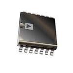
ICGOO电子元器件商城为您提供AD8567ARUZ-REEL由Analog设计生产,在icgoo商城现货销售,并且可以通过原厂、代理商等渠道进行代购。 AD8567ARUZ-REEL价格参考。AnalogAD8567ARUZ-REEL封装/规格:线性 - 放大器 - 仪表,运算放大器,缓冲器放大器, 通用 放大器 4 电路 满摆幅 14-TSSOP。您可以下载AD8567ARUZ-REEL参考资料、Datasheet数据手册功能说明书,资料中有AD8567ARUZ-REEL 详细功能的应用电路图电压和使用方法及教程。
| 参数 | 数值 |
| -3db带宽 | - |
| 产品目录 | 集成电路 (IC) |
| 描述 | IC OPAMP GP 5MHZ RRO 14TSSOP |
| 产品分类 | Linear - Amplifiers - Instrumentation, OP Amps, Buffer Amps |
| 品牌 | Analog Devices Inc |
| 数据手册 | |
| 产品图片 |
|
| 产品型号 | AD8567ARUZ-REEL |
| rohs | 无铅 / 符合限制有害物质指令(RoHS)规范要求 |
| 产品系列 | - |
| 产品培训模块 | http://www.digikey.cn/PTM/IndividualPTM.page?site=cn&lang=zhs&ptm=30008http://www.digikey.cn/PTM/IndividualPTM.page?site=cn&lang=zhs&ptm=26202 |
| 供应商器件封装 | 14-TSSOP |
| 其它名称 | AD8567ARUZ-REELDKR |
| 包装 | Digi-Reel® |
| 压摆率 | 6 V/µs |
| 增益带宽积 | 5MHz |
| 安装类型 | 表面贴装 |
| 封装/外壳 | 14-TSSOP(0.173",4.40mm 宽) |
| 工作温度 | -40°C ~ 85°C |
| 放大器类型 | 通用 |
| 标准包装 | 1 |
| 电压-电源,单/双 (±) | 4.5 V ~ 16 V |
| 电压-输入失调 | 2mV |
| 电流-电源 | 700µA |
| 电流-输入偏置 | 80nA |
| 电流-输出/通道 | 35mA |
| 电路数 | 4 |
| 视频文件 | http://www.digikey.cn/classic/video.aspx?PlayerID=1364138032001&width=640&height=505&videoID=2245193153001 |
| 输出类型 | 满摆幅 |


- 商务部:美国ITC正式对集成电路等产品启动337调查
- 曝三星4nm工艺存在良率问题 高通将骁龙8 Gen1或转产台积电
- 太阳诱电将投资9.5亿元在常州建新厂生产MLCC 预计2023年完工
- 英特尔发布欧洲新工厂建设计划 深化IDM 2.0 战略
- 台积电先进制程称霸业界 有大客户加持明年业绩稳了
- 达到5530亿美元!SIA预计今年全球半导体销售额将创下新高
- 英特尔拟将自动驾驶子公司Mobileye上市 估值或超500亿美元
- 三星加码芯片和SET,合并消费电子和移动部门,撤换高东真等 CEO
- 三星电子宣布重大人事变动 还合并消费电子和移动部门
- 海关总署:前11个月进口集成电路产品价值2.52万亿元 增长14.8%


PDF Datasheet 数据手册内容提取
16 V Rail-to-Rail Operational Amplifiers Data Sheet AD8565/AD8566/AD8567 FEATURES PIN CONFIGURATIONS Single-supply operation: 4.5 V to 16 V AD8565 Input capability beyond the rails OUT 1 5 V– Rail-to-rail output swing V+ 2 Continuous output current: 35 mA POeffaske ot uvotpltuatg ceu: r1r0e nmt:V 2 50 mA +IN 3 (NToOt Pto V SIEcWale) 4 –IN 01909-001 Figure 1. 5-Lead SC70 Pin Configuration Slew rate: 6 V/μs Unity gain stable with large capacitive loads AD8566 OUT A 1 8 V+ Supply current: 700 μA per amplifier Qualified for automotive applications –IN A 2 7 OUT B APPLICATIONS +IN A 3 6 –IN B LPCCooDrmt armebfuleenr eieclnaectceito rdnorsni veiceqsru si pment V– 4 (NToOt Pto V SIEcWale) 5 +IN B 01909-002 Figure 2. 8-Lead MSOP Pin Configuration Automotive infotainment systems GENERAL DESCRIPTION OUT A 1 14 OUT D The AD8565/AD8566/AD8567 are low cost, single-supply, rail- –IN A 2 13 –IN D to-rail input and output operational amplifiers optimized for LCD monitor applications. They are built on an advanced high +IN A 3 12 +IN D voltage CBCMOS process. The AD8565 contains a single AD8567 amplifier, the AD8566 has two amplifiers, and the AD8567 has V+ 4 TOP VIEW 11 V– (Not to Scale) four amplifiers. +IN B 5 10 +IN C These LCD op amps have high slew rates, 35 mA continuous output drive, 250 mA peak output drive, and a high capacitive –IN B 6 9 –IN C lvooaltda gdersiv bee cloapwa 1b0il imty.V T. Thehye hAaDve8 5a6 w5i/dAeD s8u5p6p6ly/A raDn8g5e6 a7n adr eo fifdseeat l OUT B 7 8 OUT C 01909-003 for LCD grayscale reference buffer and V applications. COM Figure 3. 14-Lead TSSOP Pin Configuration The AD8565/AD8566/AD8567 are specified over the −40°C to A D +85°C temperature range. The AD8565 single is available in a C UT UT C N O O N 5-lead SC70 package. The AD8566 dual is available in an 8-lead 6 5 4 3 1 1 1 1 MSOP package. The AD8567 quad is available in a 14-lead TSSOP package and a 16-lead LFCSP package. –IN A 1 12 –IN D +IN A 2 AD8567 11 +IN D The AD8566WARMZ is the automotive grade version. V+ 3 TOP VIEW 10 V– (Not to Scale) +IN B 4 9 +IN C 5 6 7 8 B B C C N T T N –I OU OU –I NOTES 1 2 .. TNCHCOE N= N ENEXOCP OTCEOSDEN DNT OEPC APTDI.N M 3U, STTH ABTE IS, V+. 01909-004 Figure 4. 16-Lead LFCSP Pin Configuration Rev. H Document Feedback Information furnished by Analog Devices is believed to be accurate and reliable. However, no responsibility is assumed by Analog Devices for its use, nor for any infringements of patents or other One Technology Way, P.O. Box 9106, Norwood, MA 02062-9106, U.S.A. rights of third parties that may result from its use. Specifications subject to change without notice. No license is granted by implication or otherwise under any patent or patent rights of Analog Devices. Tel: 781.329.4700 ©2001–2017 Analog Devices, Inc. All rights reserved. Trademarks and registered trademarks are the property of their respective owners. Technical Support www.analog.com
AD8565/AD8566/AD8567 Data Sheet TABLE OF CONTENTS Features .............................................................................................. 1 Theory of Operation .........................................................................9 Applications ....................................................................................... 1 Input Overvoltage Protection ......................................................9 General Description ......................................................................... 1 Output Phase Reversal ............................................................... 10 Pin Configurations ........................................................................... 1 Power Dissipation....................................................................... 10 Revision History ............................................................................... 2 Thermal Pad—AD8567 ............................................................. 10 Specifications ..................................................................................... 3 Total Harmonic Distortion + Noise (THD + N)........................ 11 Electrical Characteristics ............................................................. 3 Short-Circuit Output Conditions............................................. 11 Absolute Maximum Ratings ............................................................ 4 LCD Panel Applications ............................................................ 11 Thermal Resistance ...................................................................... 4 Outline Dimensions ....................................................................... 12 ESD Caution .................................................................................. 4 Ordering Guide .......................................................................... 13 Typical Performance Characteristics ............................................. 5 REVISION HISTORY 10/2017—Rev. G to Rev. H 2/2006—Rev. C to Rev. D Change to Figure 4 ........................................................................... 1 Updated Format .................................................................. Universal Changed 16-Lead LFCSP (CP-16-4) to 16-Lead LFCSP Changes to Figure 6 and Figure 8 .................................................... 5 (CP-16-23), Table 3 ........................................................................... 4 Added the Thermal Pad—AD8567 Section ................................ 10 Updated Outline Dimensions ....................................................... 13 Changes to Ordering Guide .......................................................... 13 Changes to Ordering Guide .......................................................... 13 3/2004—Rev. B to Rev. C 3/2010—Rev. F to Rev. G Changes to Specifications ................................................................. 2 Changes to Figure 4 .......................................................................... 1 Changes to TPC 4 .............................................................................. 4 Changes to the Thermal Pad—AD8567 Section ........................ 10 Changes to TPC 10 ............................................................................ 5 Changes to TPC 14 ............................................................................ 6 1/2010—Rev. E to Rev. F Changes to TPC 20 ............................................................................ 7 Changes to Applications and General Description Sections ...... 1 Changes to Figure 4 .......................................................................... 1 12/2003—Rev. A to Rev. B Added Exposed Pad Notation to Outline Dimensions ............. 12 Updated Ordering Guide ................................................................. 3 Changes to Ordering Guide .......................................................... 13 Updated Outline Dimensions ....................................................... 11 8/2007—Rev. D to Rev. E 10/2001—Rev. 0 to Rev. A Changes to Features Section............................................................ 1 Edit to 16-Lead CSP and 5-Lead SC70 Pin Configuration .......... 1 Changes to Phase Margin ................................................................ 3 Edit to Ordering Guide ..................................................................... 3 Changes to Table 2 ............................................................................ 4 Changes to Figure 30 ...................................................................... 10 7/2001—Revision 0: Initial Version Updated Outline Dimensions ....................................................... 12 Changes to Ordering Guide .......................................................... 13 Rev. H | Page 2 of 13
Data Sheet AD8565/AD8566/AD8567 SPECIFICATIONS ELECTRICAL CHARACTERISTICS 4.5 V ≤ V ≤ 16 V, V = V/2, T = 25°C, unless otherwise noted. S CM S A Table 1. Parameter Symbol Conditions Min Typ Max Unit INPUT CHARACTERISTICS Offset Voltage V 2 10 mV OS Offset Voltage Drift ΔV /ΔT −40°C ≤ T ≤ +85°C 5 µV/°C OS A Input Bias Current I 80 600 nA B −40°C ≤ T ≤ +85°C 800 nA A Input Offset Current I 1 80 nA OS −40°C ≤ T ≤ +85°C 130 nA A Input Voltage Range Common-mode input −0.5 V + 0.5 V S Common-Mode Rejection Ratio CMRR V = 0 V to V, −40°C ≤ T ≤ +85°C 54 95 dB CM S A Large Signal Voltage Gain A R = 10 kΩ, V = 0.5 V to (V − 0.5 V) 3 10 V/mV VO L O S Input Impedance Z 400 kΩ IN Input Capacitance C 1 pF IN OUTPUT CHARACTERISTICS Output Voltage High V I = 100 µA V − 0.005 V OH L S V = 16 V, I = 5 mA 15.85 15.95 V S L −40°C ≤ T ≤ +85°C 15.75 V A V = 4.5 V, I = 5 mA 4.2 4.38 V S L −40°C ≤ T ≤ +85°C 4.1 V A Output Voltage Low V I = 100 µA 5 mV OL L V = 16 V, I = 5 mA 42 150 mV S L −40°C ≤ T ≤ +85°C 250 mV A V = 4.5 V, I = 5 mA 95 300 mV S L −40°C ≤ T ≤ +85°C 400 mV A Continuous Output Current I 35 mA OUT Peak Output Current I V = 16 V 250 mA PK S POWER SUPPLY Supply Voltage V 4.5 16 V S Power Supply Rejection Ratio PSRR V = 4 V to 17 V, −40°C ≤ T ≤ +85°C 70 90 dB S A Supply Current/Amplifier I V = V/2, no load 700 850 µA SY O S −40°C ≤ T ≤ +85°C 1 mA A DYNAMIC PERFORMANCE Slew Rate SR R = 10 kΩ, C = 200 pF 4 6 V/µs L L Gain Bandwidth Product GBP R = 10 kΩ, C = 10 pF 5 MHz L L Phase Margin Ø R = 10 kΩ, C = 10 pF 65 Degrees m L L Channel Separation 75 dB NOISE PERFORMANCE Voltage Noise Density e f = 1 kHz 26 nV/√Hz n e f = 10 kHz 25 nV/√Hz n Current Noise Density i f = 10 kHz 0.8 pA/√Hz n Rev. H | Page 3 of 13
AD8565/AD8566/AD8567 Data Sheet ABSOLUTE MAXIMUM RATINGS THERMAL RESISTANCE Table 2. θ is specified for worst-case conditions, that is, for a device Parameter Rating JA soldered onto a circuit board for surface-mount packages. Supply Voltage (V) 18 V S Input Voltage −0.5 V to VS + 0.5 V Table 3. Thermal Resistance Differential Input Voltage VS Package Type θJA θJC Unit Storage Temperature Range −65°C to +150°C 5-Lead SC70 (KS-5) 376 126 °C/W Operating Temperature Range −40°C to +85°C 8-Lead MSOP (RM-8) 210 45 °C/W Junction Temperature Range −65°C to +150°C 14-Lead TSSOP (RU-14) 180 35 °C/W Lead Temperature (Soldering, 60 sec) 300°C 16-Lead LFCSP (CP-16-23) 381 301 °C/W Stresses at or above those listed under Absolute Maximum 1 DAP is soldered down to the printed circuit board (PCB). Ratings may cause permanent damage to the product. This is a ESD CAUTION stress rating only; functional operation of the product at these or any other conditions above those indicated in the operational section of this specification is not implied. Operation beyond the maximum operating conditions for extended periods may affect product reliability. Rev. H | Page 4 of 13
Data Sheet AD8565/AD8566/AD8567 TYPICAL PERFORMANCE CHARACTERISTICS 0 1000 VCM = VS/2 4.5V ≤ VS ≤ 16V TA = 25°C GE (mV) ––00..5205 Y (nV/√Hz) 100 A T FSET VOLT –0.75 VS = 4.5VVS = 16V OISE DENSI INPUT OF ––11..0205 VOLTAGE N 10 –1.50 –40 TEMPER2A5TURE (°C) 85 01909-005 110 100FREQUENCY (Hz)1k 10k 01909-008 Figure 5. Input Offset Voltage vs. Temperature Figure 8. Voltage Noise Density vs. Frequency 10 1.0 √Hz) 4T.A5 V= ≤2 5V°SC ≤ 16V mA) 0.8 VATAOV === 2+V51S°/C2 Y (pA/ FIER ( SIT PLI 0.6 N M E A E D 1 NT/ NOIS RRE 0.4 ENT Y CU R L CUR SUPP 0.2 0.110 100FREQUENCY (Hz)1k 10k 01909-006 00 2 4 S6UPPLY8 VOLT10AGE (1V2) 14 16 18 01909-009 Figure 6. Current Noise Figure 9. Supply Current/Amplifier vs. Supply Voltage 0.80 RVSL == 1160VkΩ VCM = VS/2 CL = 100pF A) 0.75 ATAV == 2+51°C ER (m VS = 16V DIV) PLIFI 0.70 mV/ AM 0 T/ 0.65 5 N ME ( RRE TI CU 0.60 Y L SUPP 0.55 VS = 4.5V FREQUENCY (1µs/DIV) 01909-007 0.50 –40 TEMPERA25TURE (°C) 85 01909-010 Figure 7. Small Signal Transient Response Figure 10. Supply Current/Amplifier vs. Temperature Rev. H | Page 5 of 13
AD8565/AD8566/AD8567 Data Sheet 100 VS = 16V VS = 16V 90 VIN = 100mV p-p 100 RL = 10kΩ 80 RALV == 1+01kΩ 80 CTAL == 2450°pCF 0 70 TA = 25°C 60 45 es) HOOT (%) 6500 –OS N (dB) 4200 91035 FT (Degre OVERS 40 +OS GAI 0 180 SE SHI A 30 225 H P 20 270 10 010 LOAD CAPA1C00ITANCE (pF) 1k 01909-011 1k 10k F1R0E0QkUENCY (1HMz) 10M 100M 01909-014 Figure 11. Small Signal Overshoot vs. Load Capacitance Figure 14. Open-Loop Gain and Phase Shift vs. Frequency 18 1k TA = 25°C 16 14 100 NG (V p-p) 1102 TAGE (mV) VS = 4.5V VS = 16V WI OL 10 T S 8 T V U U P P OUT 46 AVSV == 1+61V OUT 1 RL = 10kΩ DISTORTION < 1% 2 TA = 25°C 100 100 1kFREQU1E0NkCY (Hz)100k 1M 10M 01909-012 0.10.001 0.01 LOA0D.1 CURRENT 1(mA) 10 100 01909-015 Figure 12. Closed-Loop Output Swing vs. Frequency Figure 15. Output Voltage to Supply Rail vs. Load Current 150 4.5V ≤ VS ≤ 16V ISINK = 5mA 60 RL = 10kΩ 135 P GAIN (dB) 345000 AAVVCCLL == ––11000 CTAL == 2450°pCF TAGE (mV)11209050 VS = 4.5V OO 20 OL 75 CLOSED-L 100 AVCL = +1 OUTPUT V 6405 VS = 16V 30 15 10 100 1kFREQU1E0NkCY (Hz)100k 1M 10M 01909-013 0 –40 TEMPERA25TURE (°C) 85 01909-016 Figure 13. Closed-Loop Gain vs. Frequency Figure 16. Output Voltage Swing to Rail vs. Temperature Rev. H | Page 6 of 13
Data Sheet AD8565/AD8566/AD8567 150 160 113250 ISOURCE = 5mA VS = 4.5V O (dB) 114200 VTAS == 2156°VC E (mV)105 ON RATI 100 AG 90 CTI 80 OLT 75 EJE 60 +PSRR V R UT 60 VS = 16V LY 40 –PSRR P P OUT 45 SUP 20 R 30 WE 0 O 15 P –20 0 –40 TEMPERA25TURE (°C) 85 01909-017 –40100 1k F1R0EkQUENCY 1(0H0zk) 1M 10M 01909-020 Figure 17. Output Voltage Swing to Rail vs. Temperature Figure 20. Power Supply Rejection Ratio vs. Frequency 500 450 ATAV == 2+51°C VRSL == 1160VkΩ 400 AV = +1 TA = 25°C 350 E (Ω)300 VS = 4.5V V/DIV) C 3 AN250 E ( D G MPE200 OLTA I V 150 100 50 VS = 16V 0100 1k F1R0EkQUENCY1 (0H0zk) 1M 10M 01909-018 TIME (40µs/DIV) 01909-021 Figure 18. Closed-Loop Output Impedance vs. Frequency Figure 21. No Phase Reversal 1.8k VS = 16V VS = 16V 140 TA = 25°C 1.6k TA = 25°C 120 1.4k 100 ers)1.2k RR (dB) 6800 Y (Amplifi1.0k CM 40 NTIT800 UA600 20 Q 400 0 200 10 100 1kFREQU1E0NkCY (Hz)100k 1M 10M 01909-019 0–10 –8 –6 IN–P4UT O–F2FSET0VOLTA2GE (m4V) 6 8 10 01909-022 Figure 19. Common-Mode Rejection Ratio (CMRR) vs. Frequency Figure 22. Input Offset Voltage Distribution Rev. H | Page 7 of 13
AD8565/AD8566/AD8567 Data Sheet 5 7 4 6 A) 3 n URRENT ( 12 VS = 4.5V H (MHz) 45 SET C 0 VS = 16V DWIDT 3 UT OFF ––12 BAN 2 INP –3 AVSV == 1+61V –4 1 RTAL == 2x5°C –5 –40 TEMPERA25TURE (°C) 85 01909-023 00 2 4COMM6ON-MOD8EVOLT1A0GE (V)12 14 16 01909-026 Figure 23. Input Offset Current vs. Temperature Figure 26. Frequency vs. Common-Mode Voltage (VS = 16 V) 0 6 VCM = VS/2 VS = 5V –50 AV = +1 5 RL = 10kΩ A) VS = 16V TA = 25°C n–100 NT ( Hz) 4 E M RR–150 H ( CU VS = 4.5V DT 3 AS –200 DWI BI N UT BA 2 P–250 N I 1 –300 –350 –40 TEMPER2A5TURE (°C) 85 01909-024 00 1 COMMO2N-MODEVOL3TAGE (V) 4 5 01909-027 Figure 24. Input Bias Current vs. Temperature Figure 27. Frequency vs. Common-Mode Voltage (VS = 5 V) –20 –40 –60 dB) –80 K ( TAL–100 4.5V S S O R–120 16V C –140 –160 –180 50 100 FRE1kQUENCY (Hz) 10k 60k 01909-025 Figure 25. Channel A vs. Channel B Crosstalk Rev. H | Page 8 of 13
Data Sheet AD8565/AD8566/AD8567 THEORY OF OPERATION The AD8565/AD8566/AD8567 are designed to drive large The benefit of this type of input stage is low bias current. The capacitive loads in LCD applications. They have high output input bias current is the sum of base currents of Q4 to Q5 and current drive and rail-to-rail input/output operation and are Q6 to Q8 over the range from (V + 1 V) to (V − 1 V). NEG POS powered from a single 16 V supply. They are also intended for Outside this range, the input bias current is dominated by the other applications where low distortion and high output current sum of base currents of Q10 to Q11 for input signals close to drive are needed. V and of Q6 to Q8 (Q10 to Q11) for signals close to V . NEG POS From this type of design, the input bias current of the AD8565/ Figure 28 shows a simplified equivalent circuit for the AD8565/ AD8566/AD8567 not only exhibits different amplitude but also AD8566/AD8567. The rail-to-rail bipolar input stage is com- exhibits different polarities. Figure 29 provides the characteris- posed of two PNP differential pairs, Q4 to Q5 and Q10 to Q11, tics of the input bias current vs. the common-mode voltage. It is operating in series with diode protection networks, D1 to D2. important to keep in mind that the source impedances driving Diode network D1 to D2 serves as protection against large the inputs are balanced for optimum dc and ac performance. transients for Q4 to Q5 to accommodate rail-to-rail input swing. D5 to D6 protect Q10 to Q11 against Zenering. In normal oper- 1000 VS = 16V ation, Q10 to Q11 are off, and their input stage is buffered from 800 TA = 25°C the operational amplifier inputs by Q6 to D3 and Q8 to D4. 600 A) Operation of the input stage is best understood as a function of T (n 400 applied common-mode voltage: when the inputs of the AD8565/ REN 200 AD8566/AD8567 are biased midway between the supplies, the UR C 0 differential signal path gain is controlled by resistive loads Q4 to S A Q5 (via R9, R10). As the input common-mode level is reduced T BI–200 toward the negative supply (V or GND), the input transistor PU–400 NEG N I current sources, I1 and I2, are forced into saturation, thereby –600 forcing the Q6 to D3 and Q8 to D4 networks into cutoff. –800 However, Q4 to Q5 remain active, providing input stage gain. Inversely, when common-mode input voltage is increased –10000 2 INP4UT COM6MON-M8ODE V1O0LTAGE12 (V) 14 16 01909-029 toward the positive supply, Q4 to Q5 are driven into cutoff, Q3 Figure 29. AD8565/AD8566/AD8567 Input Bias Current vs. is driven into saturation, and Q4 becomes active, providing bias Common-Mode Voltage to the Q10 to Q11 differential pair. The point at which the Q10 to To achieve rail-to-rail output performance, the AD8565/ Q11 differential pair becomes active is approximately equal to AD8566/AD8567 design uses a complementary common- (VPOS − 1 V). source (or gmRL) output. This configuration allows output voltages to approach the power supply rails, particularly if the VPOS output transistors are allowed to enter the triode region on extremes of signal swing, which are limited by V , the R1 GS transistor sizes, and output load current. In addition, this type BIAS LINE Q3 Q4 of output stage exhibits voltage gain in an open-loop gain configuration. The amount of gain depends on the total load D1 D2 resistance at the output of the AD8565/AD8566/AD8567. R3 R4 INPUT OVERVOLTAGE PROTECTION Q6 Q8 V+ Q4 C1 Q5 V– As with any semiconductor device, whenever the input exceeds either supply voltages, attention needs to be paid to the input D3 R5 R6 D4 overvoltage characteristics. As an overvoltage occurs, the amplifier C2 could be damaged, depending on the voltage level and the Q10 Q11 magnitude of the fault current. When the input voltage exceeds D5 either supply by more than 0.6 V, internal positive-negative (pn) junctions allow current to flow from the input to the supplies. I1 D6 I2 FOLDED CASCADE R9 R10 VNEG 01909-028 Figure 28. AD8565/AD8566/AD8567 Equivalent Input Circuit Rev. H | Page 9 of 13
AD8565/AD8566/AD8567 Data Sheet This input current is not inherently damaging to the device as The power dissipated by the device can be calculated as long as it is limited to 5 mA or less. If a condition exists using P = (V − V ) × I DISS S OUT LOAD the AD8565/AD8566/AD8567 where the input exceeds the where: supply more than 0.6 V, an external series resistor must be V is the supply voltage. added. The size of the resistor can be calculated by using the S V is the output voltage. maximum over-voltage divided by 5 mA. This resistance must OUT I is the output load current. be placed in series with either input exposed to an overvoltage. LOAD Figure 30 shows the maximum power dissipation vs. temper- OUTPUT PHASE REVERSAL ature. To achieve proper operation, use the previous equation to The AD8565/AD8566/AD8567 are immune to phase reversal. calculate P for a specific package at any given temperature or DISS Although device output does not change phase, large currents use Figure 30. due to input overvoltage could damage the device. In applica- 1.25 tions where the possibility of an input voltage exceeding the supply voltage exists, overvoltage protection must be used as 16-LEAD LFCSP W) described in the Input Overvoltage Protection section. N (1.00 O POWER DISSIPATION ATI P The maximum allowable internal junction temperature of DISSI0.75 14-LEAD TSSOP R 8-LEAD MSOP 150°C limits the maximum power dissipation of AD8565/ E W AD8566/AD8567 devices. As the ambient temperature M PO0.50 5-LEAD SC70 increases, the maximum power dissipated by AD8565/AD8566/ U M AD8567 devices must decrease linearly to maintain maximum AXI0.25 M junction temperature. If this maximum junction temperature is exceeded momentarily, the device still operates properly once tmhaex jiumnuctmio nju tnecmtipoenr atetumrpe eirsa rteudrue cies de xbceeleodwe d15 f0o°rC a.n I fe xthteen ded 0–35 –15 AMB5IENTTEM2P5ERATURE45 (°C) 65 85 01909-030 Figure 30. Maximum Power Dissipation vs. Temperature for 5-Lead SC70, period, overheating could lead to permanent damage of the 8-Lead MSOP, 14-Lead TSSOP, and 16-Lead LFCSP Packages device. THERMAL PAD—AD8567 The maximum safe junction temperature, T , is 150°C. Using JMAX the following formula, the maximum power that an AD8565/ The AD8567 LFCSP comes with a thermal pad that is attached AD8566/AD8567 device can safely dissipate as a function of to the substrate. This substrate is connected to the most positive temperature can be obtained: supply, that is, Pin 3 in the LFCSP package and Pin 4 in the TSSOP package. To be electrically safe, the thermal pad must be P = T − T /θ DISS JMAX A JA soldered to an area on the board that is electrically isolated or where: connected to V . Attaching the thermal pad to ground DD PDISS is the AD8565/AD8566/AD8567 power dissipation. adversely affects the performance of the part. T is the AD8565/AD8566/AD8567 maximum allowable JMAX Soldering down this thermal pad dramatically improves the junction temperature (150°C). heat dissipation of the package. It is necessary to attach vias that T is the ambient temperature of the circuit. A connect the soldered thermal pad to another layer on the board. θ is the AD8565/AD8566/AD8567 package thermal resistance, JA This provides an avenue to dissipate the heat away from the junction-to-ambient. part. Without vias, the heat is isolated directly under the part. Rev. H | Page 10 of 13
Data Sheet AD8565/AD8566/AD8567 TOTAL HARMONIC DISTORTION + NOISE (THD + N) LCD PANEL APPLICATIONS The AD8565/AD8566/AD8567 feature low total harmonic dis- The AD8565/AD8566/AD8567 amplifier is designed for LCD tortion. Figure 31 shows THD + N vs. frequency. The THD + N panel applications or applications where large capacitive load over the entire supply range is below 0.008%. When the device drive is required. It can instantaneously source/sink greater than is powered from a 16 V supply, the THD + N stays below 250 mA of current. At unity gain, it can drive 1 μF without 0.003%. Figure 31 shows the AD8566 in a unity noninverting compensation. This makes the AD8565/AD8566/AD8567 ideal configuration. for LCD V driver applications. COM 10 To evaluate the performance of the AD8565/AD8566/AD8567, a test circuit was developed to simulate the V driver COM application for an LCD panel. Figure 32 shows the test circuit. Series capacitors and resistors connected to the output of the op 1 amp represent the load of the LCD panel. The 300 Ω and 3 kΩ %) feedback resistors are used to improve settling time. This test D+N ( circuit simulates the worst-case scenario for a VCOM. It drives a TH represented load that is connected to a signal switched symmet- 0.1 rically around V . VS = ±2.5V COM Figure 33 shows a scope photo of the instantaneous output peak VS = ±8V current capability of the AD8565/AD8566/AD8567. 0.0120 100 FREQUEN1CkY (Hz) 10k 30k 01909-031 300Ω INPUT 0VTO 8V Figure 31. THD + N vs. Frequency SQUAREWAVEWITH SHORT-CIRCUIT OUTPUT CONDITIONS 8V 3kΩ 15.6µs PULSE WIDTH 10Ω 10Ω 10Ω 10Ω The AD8565/AD8566/AD8567 do not have internal short- circuit protection circuitry. As a precautionary measure, it is 4V 10nF 10nF 10nF 10nF rpeocwoemr msuepnpdleyd o nr otot tgor oshuonrdt. t he output directly to the positive MCUERARSUENRTE 10ΩTO 20Ω 01909-032 Figure 32. VCOM Test Circuit with Supply Voltage at 16 V It is not recommended to operate the AD8565/AD8566/AD8567 with more than 35 mA of continuous output current. The output current can be limited by placing a series resistor at the output of the amplifier whose value can be derived using 100 90 V R S X 35mA CH 2 = 100mA/DIV For a 5 V single-supply operation, R must have a minimum X value of 143 Ω. CH 1 = 5V/DIV 10 0% TIME (2µs/DIV) 01909-033 Figure 33. Scope Photo of the VCOM Instantaneous Peak Current Rev. H | Page 11 of 13
AD8565/AD8566/AD8567 Data Sheet OUTLINE DIMENSIONS 3.20 3.00 2.80 8 5 5.15 3.20 4.90 3.00 4.65 2.80 1 4 PIN 1 IDENTIFIER 0.65 BSC 0.95 15° MAX 0.85 1.10 MAX 0.75 0.80 0.15 0.40 6° 0.23 0.55 CO0P.0L50A.1N0ARICTOYMPLIANT0. 2T5O JEDEC STA0°NDARDS 0M.0O9-187-AA 0.40 10-07-2009-B Figure 34. 8-Lead Mini Small Outline Package [MSOP] (RM-8) Dimensions shown in millimeters 2.20 2.00 1.80 1.35 5 4 2.40 1.25 2.10 1.15 1 2 3 1.80 0.65BSC 1.00 1.10 0.40 0.90 0.80 0.10 0.70 0.46 0.10MAX 0.30 SPELAATNIENG 00..2028 0.36 COPLANARITY 0.15 0.26 0.10 COMPLIANTTOJEDECSTANDARDSMO-203-AA 072809-A Figure 35. 5-Lead Thin Shrink Small Outline Transistor Package [SC70] (KS-5) Dimensions shown in millimeters 5.10 5.00 4.90 14 8 4.50 4.40 6.40 BSC 4.30 1 7 PIN 1 0.65 BSC 1.05 1.00 1M.2A0X 0.20 0.80 0.09 0.75 0.15 8° 0.60 0.05 0.30 SPELAATNIENG 0° 0.45 COPLANARITY 0.19 0.10 COMPLIANT TO JEDEC STANDARDS MO-153-AB-1 061908-A Figure 36. 14-Lead Thin Shrink Small Outline Package [TSSOP] (RU-14) Dimensions shown in millimeters Rev. H | Page 12 of 13
Data Sheet AD8565/AD8566/AD8567 DETAIL A (JEDEC 95) 4.10 0.35 4.00 SQ 0.30 PIN 1 3.90 0.25 INDICATOR PIN 1 0.65 13 16 1 I(NSDEEIC DAETTAOIRL AAR)EA OPTIONS BSC 12 2.25 EXPOSED 2.10 SQ PAD 1.95 9 4 0.70 8 5 0.25 MIN TOP VIEW 0.60 BOTTOM VIEW 0.50 0.80 FOR PROPER CONNECTION OF 0.75 0.05 MAX THE EXPOSED PAD, REFER TO 0.70 THE PIN CONFIGURATION AND 0.02 NOM FUNCTION DESCRIPTIONS COPLANARITY SECTION OF THIS DATA SHEET. SEATING 0.08 PLANE 0.203 REF PKG-004025/5112 COMPLIANTTOJEDEC STANDARDS MO-220-WGGC. 04-15-2016-A Figure 37. 16-Lead Lead Frame Chip Scale Package [LFCSP] 4 mm × 4 mm Body and 0.75 mm Package Height (CP-16-23) Dimensions shown in millimeters ORDERING GUIDE Model1, 2 Absolute Maximum (V) Temperature Range Package Description Package Option Branding AD8565AKSZ-REEL7 18 −40°C to +85°C 5-Lead SC70 KS-5 A0N AD8566ARMZ-R2 18 −40°C to +85°C 8-Lead MSOP RM-8 ATA# AD8566ARMZ-REEL 18 −40°C to +85°C 8-Lead MSOP RM-8 ATA# AD8566WARMZ-REEL 18 −40°C to +85°C 8-Lead MSOP RM-8 LG3 AD8567ARUZ 18 −40°C to +85°C 14-Lead TSSOP RU-14 AD8567ARUZ-REEL 18 −40°C to +85°C 14-Lead TSSOP RU-14 AD8567ACPZ-R2 18 −40°C to +85°C 16-Lead LFCSP CP-16-23 AD8567ACPZ-REEL 18 −40°C to +85°C 16-Lead LFCSP CP-16-23 AD8567ACPZ-REEL7 18 −40°C to +85°C 16-Lead LFCSP CP-16-23 1 Z = RoHS Compliant Part, # denotes RoHs compliant product, may be top or bottom marked. 2 Qualified for automotive applications. ©2001–2017 Analog Devices, Inc. All rights reserved. Trademarks and registered trademarks are the property of their respective owners. D01909-0-10/17(H) Rev. H | Page 13 of 13
Mouser Electronics Authorized Distributor Click to View Pricing, Inventory, Delivery & Lifecycle Information: A nalog Devices Inc.: AD8565AKSZ-REEL7 AD8566ARMZ-R2 AD8567ARUZ AD8566ARMZ-REEL AD8567ACPZ-R2 AD8567ACPZ- REEL AD8567ARUZ-REEL AD8566WARMZ-REEL