ICGOO在线商城 > 开发板,套件,编程器 > 评估和演示板和套件 > AD8436-EVALZ
 Datasheet下载
- 型号: AD8436-EVALZ
- 制造商: Analog
- 库位|库存: xxxx|xxxx
- 要求:
| 数量阶梯 | 香港交货 | 国内含税 |
| +xxxx | $xxxx | ¥xxxx |
查看当月历史价格
查看今年历史价格
AD8436-EVALZ产品简介:
ICGOO电子元器件商城为您提供AD8436-EVALZ由Analog设计生产,在icgoo商城现货销售,并且可以通过原厂、代理商等渠道进行代购。 AD8436-EVALZ价格参考¥968.05-¥968.05。AnalogAD8436-EVALZ封装/规格:评估和演示板和套件, AD8436 RMS to DC Converters Interface Evaluation Board。您可以下载AD8436-EVALZ参考资料、Datasheet数据手册功能说明书,资料中有AD8436-EVALZ 详细功能的应用电路图电压和使用方法及教程。
AD8436-EVALZ是Analog Devices Inc.(ADI公司)提供的一个评估板,主要用于评估AD8436差分放大器的性能。AD8436是一款高精度、低功耗的仪表放大器,具有出色的共模抑制比和增益精度,适用于需要高精度信号调理的应用场景。

 应用场景:

1. 工业自动化与控制:
   AD8436-EVALZ可以用于评估AD8436在工业自动化系统中的表现,特别是在传感器信号调理方面。例如,在温度、压力、位移等传感器中,AD8436可以将微弱的传感器输出信号进行放大和调理,确保信号的准确性和稳定性。通过AD8436-EVALZ,工程师可以轻松测试不同增益设置下的性能,并优化电路设计以满足具体应用需求。

2. 医疗设备:
   在医疗设备中,如心电图(ECG)、脑电图(EEG)等生物电信号采集系统,AD8436-EVALZ可以帮助评估AD8436在处理微弱生物电信号时的表现。AD8436的高共模抑制比和低噪声特性使其非常适合这些对信号质量要求极高的应用场景。通过该评估板,开发者可以验证AD8436在不同工作条件下的稳定性和可靠性。

3. 数据采集系统:
   AD8436-EVALZ适用于评估AD8436在各种数据采集系统中的应用,尤其是在多通道、高精度的数据采集场景中。AD8436的低功耗和高精度特性使其成为理想的选择,能够有效减少噪声干扰并提高系统的整体性能。评估板可以帮助工程师快速搭建测试平台,验证AD8436在实际应用中的表现。

4. 音频处理:
   在音频处理领域,AD8436-EVALZ可用于评估AD8436在音频信号放大和处理中的表现。AD8436的低失真和低噪声特性使其适合用于高质量音频设备的设计,如麦克风前置放大器、音频混音器等。通过评估板,开发人员可以测试AD8436在不同音频信号范围内的性能,确保其满足音频设备的严格要求。

5. 电力监控:
   在电力监控系统中,AD8436-EVALZ可以帮助评估AD8436在电流和电压测量中的应用。AD8436的高共模抑制比和宽输入范围使其能够精确测量电力线上的微小变化,确保电力监控系统的准确性。评估板允许用户在不同负载条件下测试AD8436的性能,优化电力监控系统的电路设计。

总之,AD8436-EVALZ为工程师提供了一个便捷的工具,帮助他们在多种应用场景中评估AD8436的性能,从而加速产品开发和优化设计。
| 参数 | 数值 |
| 产品目录 | 编程器,开发系统半导体 |
| 描述 | BOARD EVAL FOR AD8436电源管理IC开发工具 AD8436 EVAL Brd |
| 产品分类 | |
| 品牌 | Analog Devices |
| 产品手册 | |
| 产品图片 |
|
| rohs | 符合RoHS无铅 / 符合限制有害物质指令(RoHS)规范要求 |
| 产品系列 | 电源管理IC开发工具,Analog Devices AD8436-EVALZ- |
| 数据手册 | |
| 产品型号 | AD8436-EVALZ |
| 主要属性 | - |
| 主要用途 | 接口,RMS 到 DC 转换器 |
| 产品 | Evaluation Boards |
| 产品培训模块 | http://www.digikey.cn/PTM/IndividualPTM.page?site=cn&lang=zhs&ptm=25912 |
| 产品种类 | 电源管理IC开发工具 |
| 使用的IC/零件 | AD8436 |
| 其它名称 | AD8436EVALZ |
| 商标 | Analog Devices |
| 封装 | Bulk |
| 嵌入式 | - |
| 工具用于评估 | AD8436 |
| 工厂包装数量 | 1 |
| 所含物品 | 板 |
| 最大工作温度 | + 125 C |
| 最小工作温度 | - 40 C |
| 标准包装 | 1 |
| 特色产品 | http://www.digikey.cn/product-highlights/cn/zh/analog-devices-ad8436-rms-dc-converter/3512 |
| 类型 | Power Management Specialized |
| 系列 | AD8436 |
| 辅助属性 | - |
| 输入电压 | + / - 18 V |


- 商务部:美国ITC正式对集成电路等产品启动337调查
- 曝三星4nm工艺存在良率问题 高通将骁龙8 Gen1或转产台积电
- 太阳诱电将投资9.5亿元在常州建新厂生产MLCC 预计2023年完工
- 英特尔发布欧洲新工厂建设计划 深化IDM 2.0 战略
- 台积电先进制程称霸业界 有大客户加持明年业绩稳了
- 达到5530亿美元!SIA预计今年全球半导体销售额将创下新高
- 英特尔拟将自动驾驶子公司Mobileye上市 估值或超500亿美元
- 三星加码芯片和SET,合并消费电子和移动部门,撤换高东真等 CEO
- 三星电子宣布重大人事变动 还合并消费电子和移动部门
- 海关总署:前11个月进口集成电路产品价值2.52万亿元 增长14.8%

PDF Datasheet 数据手册内容提取
Low Cost, Low Power, True RMS-to-DC Converter Data Sheet AD8436 FEATURES FUNCTIONAL BLOCK DIAGRAM Delivers true rms or average rectified value of ac waveform CAVG CCF Fast settling at all input levels VCC AD8436 Accuracy: ±10 μV ± 0.25% of reading (B grade) 100kΩ SUM Wide dynamic input range IGND 100 μV rms to 3 V rms (8.5 V p-p) full-scale input range RMS 8kΩ RMS CORE 100kΩ Larger inputs with external scaling VEE OGND Wide bandwidth: 16kΩ 1 MHz for −3 dB (300 mV) 10pF OUT 65 kHz for additional 1% error Zero converter dc output offset 10kΩ 10kΩ IBUFGN No residual switching products Specified at 300 mV rms input IBUFIN– – IBUFOUT Accurate conversion with crest factors up to 10 IBUFIN+ + FET OP AMP Low power: 300 µA typical at ±2.4 V High-Z FET separately powered input buffer OBUFIN+ + DC BUFFER PreciRsIiNo ≥n 1d0c1 o2 uΩt,p CuINt ≤b u2f fpeFr OBUFIN– 16kΩ – OBUFOUT 10033-001 Wide power supply voltage range Figure 1. Dual: ±2.4 V to ±18 V; single: 4.8 V to 36 V 4 mm × 4 mm LFCSP and 8 mm × 6 mm QSOP packages ESD protected GENERAL DESCRIPTION The AD8436 is a new generation, translinear precision, low The precision dc output buffer minimizes errors when driving power, true rms-to-dc converter loaded with options. It computes a low impedance loads with extremely low offset voltages, thanks precise dc equivalent of the rms value of ac waveforms, including to internal bias current cancellation. Unlike digital solutions, the complex patterns such as those generated by switch mode power AD8436 has no switching circuitry limiting performance at high or supplies and triacs. Its accuracy spans a wide range of input levels low amplitudes (see Figure 2). A usable response of <100 μV (see Figure 2) and temperatures. The ensured accuracy of ≤±0.5% and >3 V extends the dynamic range with no external scaling, and ≤10 μV output offset result from the latest Analog Devices, accommodating demanding low level signal conditions and Inc., technology. The crest factor error is <0.5% for CF values allowing ample overrange without clipping. between 1 and 10. GREATER INPUT DYNAMIC RANGE The AD8436 delivers true rms results at less cost than misleading peak, averaging, or digital solutions. There is no programming AD8436 expense or processor overhead to consider, and the 4 mm 4 mm package easily fits into tight applications. On-board buffer ∆Σ SOLUTION amplifiers enable the widest range of options for any rms-to-dc converter available, regardless of cost. For minimal applications, 100µV 1mV 10mV 100mV 1V 3V 10033-002 only a single external averaging capacitor is required. The built-in Figure 2. Usable Dynamic Range of the AD8436 vs. ΔΣ high impedance FET buffer provides an interface for external The AD8436 operates from single or dual supplies of ±2.4 V attenuators, frequency compensation, or driving low impedance (4.8 V) to ±18 V (36 V). A and J grades are available in a compact loads. A matched pair of internal resistors enables an easily 4 mm × 4 mm, 20-lead chip-scale package; A and B grades are configurable gain-of-two or more, extending the usable input available in a 20-lead QSOP package. The operating temperature range even lower. The low power, precision input buffer makes ranges are −40°C to 125°C for A and B grades and 0°C to 70°C the AD8436 attractive for use in portable multi-meters and for J grade. other battery-powered applications. Rev. E Document Feedback Information furnished by Analog Devices is believed to be accurate and reliable. However, no responsibility is assumed by Analog Devices for its use, nor for any infringements of patents or other One Technology Way, P.O. Box 9106, Norwood, MA 02062-9106, U.S.A. rights of third parties that may result from its use. Specifications subject to change without notice. No license is granted by implication or otherwise under any patent or patent rights of Analog Devices. Tel: 781.329.4700 ©2011–2017 Analog Devices, Inc. All rights reserved. Trademarks and registered trademarks are the property of their respective owners. Technical Support www.analog.com
AD8436 Data Sheet TABLE OF CONTENTS Features .............................................................................................. 1 Theory of Operation ...................................................................... 10 Functional Block Diagram .............................................................. 1 Overview ..................................................................................... 10 General Description ......................................................................... 1 Applications Information .............................................................. 12 Revision History ............................................................................... 2 Using the AD8436 ...................................................................... 12 Specifications ..................................................................................... 3 Additional Information ............................................................. 15 Absolute Maximum Ratings ............................................................ 4 AD8436 Evaluation Board ............................................................ 17 ESD Caution .................................................................................. 4 Outline Dimensions ....................................................................... 20 Pin Configurations and Function Descriptions ........................... 5 Ordering Guide .......................................................................... 21 Typical Performance Characteristics ............................................. 6 Test Circuits ....................................................................................... 9 REVISION HISTORY 3/2017—Rev. D to Rev. E 7/2012—Rev. 0 to Rev. A Changed CP-20-10 to CP-20-8 .................................... Throughout Added 20-Lead QSOP ....................................................... Universal Changes to Outline Dimensions ................................................... 21 Changes to Features Section and General Description Section .. 1 Changes to Ordering Guide .......................................................... 22 Changes to Table 1 ............................................................................. 3 Changes to Table 2 ............................................................................. 4 10/2015—Rev. C to Rev. D Changes to Table 3 and added Figure 4 and added Table 4; Changes to Figure 5 to Figure 8 ...................................................... 6 Renumbered Sequentially ................................................................ 5 Changes to Equation 1 and change to Column One Heading 7/2015—Rev. B to Rev. C in Table 5 .......................................................................................... 10 Changes to Table 2 ............................................................................ 4 Changes to Averaging Capacitor Considerations—RMS Changes to Figure 5 to Figure 7 ...................................................... 6 Accuracy and to Post Conversion Ripple Reduction Filter Changes to Figure 21 ........................................................................ 9 and changes to Figure 27 Caption ................................................ 12 Changes to Using the FET Input Buffer Section ........................ 14 Changes to Figure 30 to Figure 32 ................................................ 13 Changes to Single-Supply Section and Figure 39 ....................... 15 Changes to Using the FET Input Buffer Section and Using the Added Additional Information Section ....................................... 15 Output Buffer Section .................................................................... 14 Changes to AD8436 Evaluation Board Section and A Word Changes to Figure 38 and Figure 41 and added Converting About Using the AD8436 Evaluation Board Section ................... 17 to Rectified Average Value Section .............................................. 15 Added Single-Supply Operation Section ..................................... 17 Changes to Figure 41 ...................................................................... 16 Changes to Ordering Guide .......................................................... 21 Changes to Figure 42 to Figure 46 ................................................ 17 Changes to Figure 47 and Figure 48............................................. 18 1/2013—Rev. A to Rev. B Updated Outline Dimensions ....................................................... 19 Added B Grade Throughout ............................................. Universal Changes to Ordering Guide .......................................................... 20 Changes to Figure 1 and changes to General Description .......... 1 Changes to Table 1 ............................................................................ 3 7/2011—Revision 0: Initial Version Changes to Figure 3 ......................................................................... 5 Changes to Figure 9 and Figure 10 ................................................. 6 Changes to FET Input Buffer Section .......................................... 11 Changes to Averaging Capacitor Considerations—RMS Accuracy Section and changes to Figure 28 ................................ 12 Deleted Capacitor Construction Section; added CAVG Capacitor Styles Section ................................................................. 13 Added Converting to Average Rectified Value Section ............. 15 Changes to Figure 41 ...................................................................... 16 Changes to Evaluation Board Section .......................................... 17 Changes to Figure 48 ...................................................................... 19 Changes to Outline Dimensions ................................................... 20 Changes to Ordering Guide .......................................................... 21 Rev. E | Page 2 of 21
Data Sheet AD8436 SPECIFICATIONS e = 300 mV (rms), frequency = 1 kHz sinusoidal, ac-coupled, ±V = ±5 V, T = 25°C, C = 10 μF, unless otherwise specified. IN S A AVG Table 1. AD8436A, AD8436J AD8436B Parameter Test Conditions/Comments Min Typ Max Min Typ Max Unit RMS CORE Conversion Error Default conditions ±10 − 0.5 ±0 ± 0 ±10 + 0.5 ±10 − 0.25 ±0 ± 0 ±10 + 0.25 μV/% rdg Vs. Temperature −40°C < T < 125 C 0.006 0.006 %/°C Vs. Rail Voltage ±2.4 V to ±18 V ±0.013 ±0.013 ±%/V Input VOS DC-coupled −500 0 +500 −250 0 +250 μV Output VOS AC-coupled input 0 0 V Vs. Temperature −40 C < T < 125°C 0.3 0.3 μV/°C DC Reversal Error DC-coupled, VIN = ±300 mV −1.5 0 +1.5 −1.0 0 +1.0 % Nonlinearity eIN = 2 mV to 500 mV ac ±0.2 ±0.2 % Crest Factor Error (Additional) 1 < CF < 10 CCF = 0.1 μF −0.5 +0.5 −0.5 +0.5 % Peak Input Voltage −VS − 0.7 +VS + 0.7 −VS − 0.7 +VS + 0.7 V Input Resistance 7.92 8 8.08 7.92 8 8.08 kΩ Response VIN = 300 mV rms 1% Error (Additional) 65 65 kHz 3 dB Bandwidth 1 1 MHz Settling Time 0.1% Rising/falling 148/341 148/341 ms 0.01% Rising/falling 158/350 158/350 ms Output Resistance 15.68 16 16.32 15.68 16 16.32 kΩ Supply Current No input 325 365 325 365 μA INPUT BUFFER Voltage Swing G = 1 Input AC- or dc-coupled −VS +VS −VS +VS V Output AC-coupled to Pin RMS −VS + 0.2 +VS − 0.2 −VS + 0.2 +VS − 0.2 mV Offset Voltage −1 0 +1 −0.5 0 +0.5 mV Input Bias Current 50 50 pA Input Resistance 1012 1012 Ω Response (Frequency) 0.1 dB 950 950 kHz 3 dB Bandwidth 2.1 2.1 MHz Supply Current 100 160 200 100 160 200 μA Optional Gain Resistor −9.9 +10 +10.1 −9.9 +10 +10.1 kΩ Gain Error G = ×1 0.05 0.05 % OUTPUT BUFFER RL = Offset Voltage Connected to Pin OUT −200 0 +200 −150 0 +150 μV Input Current (IB) 2 51 2 51 nA Output Swing (Voltage) −VS + 50e−6 +VS − 1 −VS + 50e−6 +VS − 1 V Output Drive Current −0.5 (sink) +15 (source) −0.5 (sink) +15 (source) mA Gain Error 0.003 0.01 0.003 0.01 % Supply Current 40 70 40 70 μA SUPPLY VOLTAGE Dual ±2.4 ±18 ±2.4 ±18 V Single 4.8 36 4.8 36 V 1 IB max measured at power up. Settles to typical value in <15 seconds. Rev. E | Page 3 of 21
AD8436 Data Sheet ABSOLUTE MAXIMUM RATINGS Table 2. Stresses at or above those listed under Absolute Maximum Parameter Rating Ratings may cause permanent damage to the product. This is a Voltage stress rating only; functional operation of the product at these Supply Voltage ±18 V or any other conditions above those indicated in the operational Input Voltage Range1 VEE − 0.3 V to VCC + 0.3 V section of this specification is not implied. Operation beyond Differential Input VCC and VEE the maximum operating conditions for extended periods may Current affect product reliability. Input Current1 ±10 mA ESD CAUTION Output Short-Circuit Duration Indefinite Power Dissipation CP-20-8 LFCSP Without Thermal Pad 1.2 W CP-20-8 LFCSP With Thermal Pad 2.1 W RQ Package 1.1 W Temperature Operating Range −40°C to +125°C Storage Range −65°C to +125°C Lead Soldering (60 sec) 300°C θ 2 JA CP-20-8 LFCSP Without Thermal Pad 86°C/W CP-20-8 LFCSP With Thermal Pad 48°C/W RQ-20 Package 95°C/W ESD Rating 2 kV 1 Input pins have clamp diodes to the power supply pins. Limit input current to 10 mA or less whenever input signals exceed the power supply rail by 0.3 V. 2 θJA is specified for the worst-case conditions, that is, a device soldered in a circuit board for surface-mount packages. Rev. E | Page 4 of 21
Data Sheet AD8436 PIN CONFIGURATIONS AND FUNCTION DESCRIPTIONS SUM CAVG CCF VCC IBUFV+ SUM 1 20 CAVG 20 16 1 15 DNC 2 19 CCF DNC OBUFV+ RMS 3 18 VCC AD8436 IBUFOUT 4 17 IBUFV+ PIN1 TOP VIEW RMS INDICATOR OBUFOUT IBUFIN– 5 (Not to Scale) 16 OBUFV+ IBUFIN+ 6 15 OBUFOUT AD8436 IBUFGN 7 14 OBUFIN– TOP VIEW IBUFOUT (Not to Scale) OBUFIN– DNC 8 13 OBUFIN+ OGND 9 12 IGND IBUFIN– OBUFIN+ OUT 10 11 VEE IBUFIN+ 5 11 IGND N1 . O DDTNOEC SN =O DT OC ONNONTE CCOTN TNOE CTTH.IS PIN. 10033-104 6 10 IBUFGN DNC OGND OUT VEE N12..O TDTHNEECS E=X DPOO SNEODT PCAODN NCEOCNTN.E DCOT INOONT I SC OONPNTIEOCNTA TLO. THIS PIN. 10033-003 Figure 3. Pin Configuration, Top View, CP-20-8 Figure 4. Pin Configuration, RQ-20 Table 3. Pin Function Descriptions, CP-20-8 Table 4. Pin Function Descriptions, RQ-20 Pin No. Mnemonic Description Pin No. Mnemonic Description 1 DNC Do Not Connect. Used for factory test. 1 SUM Summing Amplifier Input Pin. 2 RMS AC Input to the RMS Core. 2 DNC Do Not Connect. Used for factory test. 3 IBUFOUT FET Input Buffer Output Pin. 3 RMS AC Input to the RMS Core. 4 IBUFIN− FET Input Buffer Inverting Input Pin. 4 IBUFOUT FET Input Buffer Output Pin. 5 IBUFIN+ FET Input Buffer Noninverting Input Pin. 5 IBUFIN− FET Input Buffer Inverting Input Pin. 6 IBUFGN Optional 10 kΩ Precision Gain Resistor. 6 IBUFIN+ FET Input Buffer Noninverting Input Pin. 7 DNC Do Not Connect. Used for factory test. 7 IBUFGN Optional 10 kΩ Precision Gain Resistor. 8 OGND Internal 16 kΩ I-to-V Resistor. 8 DNC Do Not Connect. Used for factory test. 9 OUT RMS Core Voltage or Current Output. 9 OGND Internal 16 kΩ I-to-V Resistor. 10 VEE Negative Supply Rail. 10 OUT RMS Core Voltage or Current Output. 11 IGND Half Supply Node. 11 VEE Negative Supply Rail. 12 OBUFIN+ Output Buffer Noninverting Input Pin. 12 IGND Half Supply Node. 13 OBUFIN− Output Buffer Inverting Input Pin. 13 OBUFIN+ Output Buffer Noninverting Input Pin. 14 OBUFOUT Output Buffer Output Pin. 14 OBUFIN− Output Buffer Inverting Input Pin. 15 OBUFV+ Power Pin for the Output Buffer. 15 OBUFOUT Output Buffer Output Pin. 16 IBUFV+ Power Pin for the Input Buffer. 16 OBUFV+ Power Pin for the Output Buffer. 17 VCC Positive Supply Rail for the RMS Core. 17 IBUFV+ Power Pin for the Input Buffer. 18 CCF Connection for Crest Factor Capacitor. 18 VCC Positive Supply Rail for the RMS Core. 19 CAVG Connection for Averaging Capacitor. 19 CCF Connection for Crest Factor Capacitor. 20 SUM Summing Amplifier Input Pin. 20 CAVG Connection for Averaging Capacitor. EP DNC Exposed Pad Connection to Ground Pad Optional. Rev. E | Page 5 of 21
AD8436 Data Sheet TYPICAL PERFORMANCE CHARACTERISTICS T = 25°C, ±V = ±5 V, C = 10 μF, 1 kHz sine wave, unless otherwise indicated. A S AVG 5V 5V C) VD VS = ±5V s; 1V 1V m S (V r ms) GE100mV V r 100mV OLTA VEL ( OUTPUT V 10mV INPUT LE 10mV −3dB ERROR ND 1mV 1mV A UT ±1% ERROR INP 100µV ±–130d%B EERRRROORR 100µV VS = 4.8V 50µV50100 1k FREQU10EkNCY (Hz)100k 1M 5M 10033-004 50µV50100 1k FREQU10EkNCY (Hz)100k 1M 5M 10033-007 Figure 5. RMS Core Frequency Response (See Figure 21) Figure 8. RMS Core Frequency Response with VS = +4.8 V (See Figure 22) 5V 15 C) eIN = 3.5mV rms D 12 s; V 1V m 9 V r GAIN = 6dB ES (100mV 6 G PUT VOLTA 10mV GAIN (dB) –303 GAIN = 0dB T U O ±1% ERROR –6 ND 1mV ±10% ERROR A –3dB ERROR –9 T U P –12 IN 100µV VS = ±2.4V 50µV50100 1k FREQU10EkNCY (Hz)100k 1M 5M 10033-005 –15100 1k FR1E0QkUENCY (H1z0)0k 1M 5M 10033-008 Figure 6. RMS Core Frequency Response with VS = ±2.4 V (See Figure 21) Figure 9. Input Buffer, Small Signal Bandwidth at 0 dB and 6 dB Gain 5V 15 C) eIN = 300mV rms D 12 s; V 1V m 9 V r GAIN = 6dB ES ( 100mV 6 G PUT VOLTA 10mV GAIN (dB) –303 GAIN = 0dB T U O –6 D 1mV ±1% ERROR N ±10% ERROR T A –3dB ERROR –9 U P –12 IN 100µV VS = ±15V 50µV50100 1k FREQU10EkNCY (Hz)100k 1M 5M 10033-006 –15100 1k FR1E0QkUENCY (H1z0)0k 1M 5M 10033-009 Figure 7. RMS Core Frequency Response with VS = ±15 V (See Figure 21) Figure 10. Input Buffer, Large Signal Bandwidth at 0 dB and 6 dB Gain Rev. E | Page 6 of 21
Data Sheet AD8436 15 10 eIN = 3.5mV rms PW = 100µs 12 G) 9 DIN A 5 6 RE F N (dB) 03 OR (% O 0 CCCAFV G= =0 .110µµFF AI R G –3 ER L CAVG = 10µF A –6 N –9 DITIO −5 D A –12 –15100 1k FR1E0QkUENCY (H1z0)0k 1M 5M 10033-010 −100 2 CRES4T FACTOR R6ATIO 8 10 10033-013 Figure 11. Output Buffer, Small Signal Bandwidth Figure 14. Crest Factor Error vs. Crest Factor for CAVG and CAVG and CCF Capacitor Combinations 0.5 1.00 CAVG=10µF 0.4 8 SAMPLES G) 0.75 N %) 0.3 EADI 0.50 RROR ( 00..21 % OF R 0.25 D E R ( ZE 0 RO 0 MALI –0.1 L ER−0.25 R A O N N –0.2 O TI−0.50 –0.3 DDI A−0.75 –0.4 –0.50 2 4 6SUPP8LY VO10LTAG1E2 (±V)14 16 18 20 10033-011 −1.00–50 –25 0 TEMP25ERATUR5E0 (°C) 75 100 125 10033-014 Figure 12. Additional Error vs. Supply Voltage Figure 15. Additional Conversion Error vs. Temperature 2.0 2.5 1.6 2.0 s) A) VS = ±15V m m VEL (V r 1.2 RRENT ( 1.5 VS = ±5V INPUT LE 0.8 UPPLY CU 1.0 VS = ±2.4V S 0.4 0.5 00 2 4 S6UPPLY8 VOLT1A0GE (±1V2) 14 16 18 10033-012 00 0.5 INPUT VOL1T.A0GE (V rms) 1.5 2.0 10033-015 Figure 13. Core Input Voltage for 1% Error vs. Supply Voltage Figure 16. RMS Core Supply Current vs. Input for VS = ±2.4 V, ±5 V, and ±15 V Rev. E | Page 7 of 21
AD8436 Data Sheet 90 250 80 200 70 V) 150 µ A) 60 GE ( 100 p A T ( 50 LT 50 N O S CURRE 4300 FFSET V −500 A O BI 20 UT −100 P 10 IN −150 0 −200 −10−50 −25 0 TEMP2E5RATUR5E0 (°C) 75 100 125 10033-016 −250−50 −25 0 TEMP2E5RATURE50 (°C) 75 100 125 10033-019 Figure 17. FET Input Buffer Bias Current vs. Temperature Figure 19. Output Buffer VOS vs. Temperature 1000 CAVG = 10µF 750 1kHz 300mV rms BURST INPUT 0V µV) 500 E ( G A 250 T L O ET V 0 300mV DC OUT S FF −250 O 0V T U P −500 N 1kHz 1mV rms BURST INPUT I 0V −750 −1000−50 −25 0 TEM2P5ERATUR50E (°C) 75 100 125 10033-018 1mV DC TOIMUET (50ms/DIV) 0V 10033-020 Figure 18. Input Offset Voltage of FET Buffer vs. Temperature Figure 20. Transition Times with 1 kHz Burst at Two Input Levels (See Theory of Operation Section) Rev. E | Page 8 of 21
Data Sheet AD8436 TEST CIRCUITS CALIBRATOR (50Hz<f<500kHz) eINA T= T1E0N0µUVA,T 3O00RµV 10µF +5V CAV VCC 100kΩ 22µF RMS IGND PRECISION DMM RMS CORE FUNCTION GENERATOR (f>500kHz) 100kΩ 16kΩ OGND OUT VEE PRECISION DMM –5V 10µF 10033-021 Figure 21. Core Response Test Circuit Using Dual Supplies SIGNAL SOURCE 10µF 4.80V CAV VCC 4.7µF RMS RMS CORE 100kΩ IGND AC-IN MONITOR 4.7µF 100kΩ 16kΩ PRECISION DMM OUT OGND VEE PRECISION DMM 10033-022 Figure 22. Core Response Test Circuit Using a Single Supply 10µF +5V FUNCTION GENERATOR CAV VCC 4.7µF RMS RMS CORE 100kΩ IGND AC-IN MONITOR 100kΩ 16kΩ PRECISION DMM OUT OGND VEE –5V PRECISION DMM 10033-023 Figure 23. Crest Factor Test Circuit Rev. E | Page 9 of 21
AD8436 Data Sheet THEORY OF OPERATION OVERVIEW RMS Core The AD8436 is an implicit function rms-to-dc converter that The core consists of a voltage-to-current converter (precision renders a dc voltage dependent on the rms (heating value) of an resistor), absolute value, and translinear sections. The translinear ac voltage. In addition to the basic converter, this highly integrated section exploits the properties of the bipolar transistor junctions functional circuit block includes two fully independent, optional for squaring and root extraction (see Figure 24). The external amplifiers, a standalone FET input buffer amplifier, and a precision capacitor (CAVG) provides for averaging the product. Figure 20 dc output buffer amplifier (see Figure 1). The rms core includes shows that there is no effect of signal input on the transition times, a precision current responding full-wave rectifier and a log- as seen in the dc output. Although the rms core responds to input antilog transistor array for current squaring and square rooting voltages, the conversion process is current sensitive. If the rms to implement the classic expression for rms (see Equation 1). input is ac-coupled, as recommended, there is no output offset For basic applications, the converter requires only an external voltage, as reflected in Table 1. If the rms input is dc-coupled, the capacitor, for averaging (see Figure 31). The optional on-board input offset voltage is reflected in the output and can be calibrated amplifiers offer utility and flexibility in a variety of applications as with any fixed error. without incurring additional circuit board footprint. For lowest V+ power, the amplifier supply pins are left unconnected. Why RMS? The rms value of an ac voltage waveform is equal to the dc + – voltage providing the same heating power to a load. A common OUT measurement technique for ac waveforms is to rectify the signal 5kΩ CAVG iinn ath set raaviegrhatgfoer vwaalurde. wTahye uasvienrga gae d viaolduee aorfr vayar oiof usos mweav seofrotr, mress u(sltinineg, ACIN ABVSAOLLUUETE V+ 16kΩ V-TO-I CIRCUIT square, and triangular, for example) varies widely; true rms is the only metric that achieves equivalency for all ac waveforms. See Table 5 for non-rms-responding circuit errors. The acronym rms means “root-mean-square” and reads as follows: V– 10033-024 “the square root of the average of the sum of the squares” of the Figure 24. RMS Core Block Diagram peak values of any waveform. RMS is shown in the following equation: 1T 2 e Vtdt (1) rms T 0 For additional information, select Section I of the second edition of the Analog Devices RMS-to-DC Applications Guide. Table 5. General AC Parameters Reading of an Average Value Circuit Waveform Type (1 V Peak) Crest Factor RMS Value Calibrated to an RMS Sine Wave Error (%) Sine 1.414 0.707 0.707 0 Square 1.00 1.00 1.11 11.0 Triangle 1.73 0.577 0.555 −3.8 Noise 3 0.333 0.295 Rectangular 2 0.5 0.278 −11.4 Pulse 10 0.1 0.011 −44 SCR −89 DC = 50% 2 0.495 0.354 −28 DC = 25% 4.7 0.212 0.150 −30 Rev. E | Page 10 of 21
Data Sheet AD8436 The 16 kΩ resistor in the output converts the output current to The output buffer can be configured as a single or two-pole low- a dc voltage that can connect to the output buffer or to the pass filter using circuits shown in the Applications Information circuit that follows. The output appears as a voltage source in section. Residual output ripple is reduced, without affecting the series with 16 kΩ. If a current output is desired, the resistor converted dc output. As the response approaches the low frequency connection to ground is left open and the output current is end of the bandwidth, the ripple rises, dependent on the value applied to a subsequent circuit, such as the summing node of of the averaging capacitor. Figure 27 shows the effects of four a current summing amplifier. Thus, the core has both current combinations of averaging and filter capacitors. Although the and voltage outputs, depending on the configuration. For a filter capacitor reduces the ripple for any given frequency, the dc voltage output with 0 Ω source impedance, use the output error is unaffected. Of course, a larger value averaging capacitor can buffer. The offset voltage of the buffer is 25 μV or 50 μV, be selected, at a larger cost. The advantage of using a low-pass filter depending on the grade. is that a small value of filter capacitor, in conjunction with the 16 kΩ output resistor, reduces ripple and permits a smaller FET Input Buffer averaging capacitor, effecting a cost savings. The recommended Because the V-to-I input resistor value of the AD8436 rms core capacitor values for operation to 40 Hz are 10 μF for averaging is 8 kΩ, a high input impedance buffer is often used between and 3.3 μF for filter. rms-to-dc converters and finite impedance sources. The optional Dynamic Range JFET input op amp minimizes attenuation and uncouples common input amenities, such as resistive voltage dividers or resistors used The AD8436 is a translinear rms-to-dc converter with exceptional to terminate current transformers. The wide bandwidth of the dynamic range. Although accuracy varies slightly more at the FET buffer is well matched to the rms core bandwidth so that extreme input values, the device still converts with no spurious no information is lost due to serial bandwidth effects. Although noise or dropout. Figure 25 is a plot of the rms/dc transfer function the input buffer consumes little current, the buffer supply is near zero voltage. Unlike processor or other solutions, residual independently accessible and can disconnect to reduce power. errors at very low input levels can be disregarded for most applications. Optional matched 10 kΩ input and feedback resistors are provided on chip. Consult the Applications Information section to learn 30 how to use these resistors. The 3 dB bandwidth of the input C) D buffer is 2.7 MHz at 10 mV rms input and approximately 1.5 MHz mV ∆Σ OR OTHER DIGITAL at 1 V rms. The amplifier gain and bandwidth are sufficient for E ( 20 SOWLUOTRIOK NAST CZAENRNOOT applications requiring modest gain or response enhancement to TAG VOLTS L a few hundred kilohertz (kHz), if desired. Configurations of the VO T 10 input buffer are discussed in the Applications Information section. U P UT AD8436 Precision Output Buffer O SOLUTION Ttrhime mpreedci tsoio cna noucetpl uintp buutf ofefrfs iest a v boilptaoglea re rinroprust. aAms pwliitfhie rt,h lea sinerp ut 0–30 –20 –I1N0PUT VOLTA0GE (mV DC1)0 20 30 10033-025 buffer, the supply current is very low (<50 μA, typically), and Figure 25. DC Transfer Function near Zero the power can be disconnected for power savings if the buffer is not needed. Be sure that the noninverting input is also disconnected from the core output (OUT) if the buffer supply pin is disconnected. Although the input current of the buffer is very low, a laser-trimmed 16 kΩ resistor, connected in series with the inverting input, offsets any self-bias offset voltage. Rev. E | Page 11 of 21
AD8436 Data Sheet APPLICATIONS INFORMATION USING THE AD8436 Ripple is reduced by increasing the value of the averaging capacitor, or by postconversion filtering. Ripple reduction This section describes the power supply and feature options, following conversion is far more efficient because the ripple as well as the function and selection of averaging and filter average value has converted to its rms value. Capacitor values for capacitor values. Averaging and filtering options are shown post-conversion filtering are significantly less than the equivalent graphically and apply to all circuit configurations. averaging capacitor value for the same level of ripple reduction. Averaging Capacitor Considerations—RMS Accuracy This approach requires only a single capacitor connected to the Typical AD8436 applications require only a single external OUT pin (see Figure 26). The capacitor value correlates to the capacitor (CAVG) connected to the CAVG pin (see Figure 31). simple frequency relation of ½ π R-C, where R is fixed at 16 kΩ. The function of the averaging capacitor is to compute the mean (that is, average value) of the sum of the squares. Averaging OUT CORE 9 DC OUTPUT (that is, integration) follows the rms core, where the input CLPF current is squared. The mean value is the average value of the 16kΩ OGND srmqusa errerdo ri nisp duitr evcotlltya gafef eocvteedr sbeyv tehrea ln iunmpubte rw oafv pefeorriomd sp aevreioradgse. dT, haes 8 10033-026 is the resultant peak-to-peak ripple. Figure 26. Simple One-Pole Post Conversion Filter The result of the conversion process is a dc component and a As seen in Figure 27, CAVG alone determines the rms error, and ripple component whose frequency is twice that of the input. The CLPF serves purely to reduce ripple. Figure 27 shows a constant rms conversion accuracy depends on the value of CAVG, so the rms error for CLPF values of 0.33 μF and 3.3 μF; only the ripple value selected need only be large enough to average enough periods is affected. at the lowest frequency of interest to yield the required rms 1 CAVG = 10µF accuracy. CLPF = 0.33µF OR 3.3µF 0 Figure 28 is a plot of rms error vs. frequency for various averaging –1 capacitor values. To use Figure 28, simply locate the frequency –2 of interest and acceptable rms error on the horizontal and vertical scales, respectively. Then choose or estimate the next highest –3 capacitor value adjacent to where the frequency and error lines R (%) –4 intersect (for an example, see the orange circle in Figure 28). O RR –5 Post Conversion Ripple Reduction Filter MS E –6 Input rectification included in the AD8436 introduces a residual R CAVG = 1µF –7 CLPF = 0.33µF OR 3.3µF ripple component that is dependent on the value of CAVG and –8 twice the input signal frequency for symmetrical input waveforms. –9 For sampling applications such as a high resolution ADC, the ripple cdoismpplaoyn neuntm meraayl sc atou sfela oshn.e or more LSBs to cycle, and low value –1010 FREQUE1N0C0Y (Hz) 1k 10033-027 Figure 27. RMS Error vs. Frequency for Two Values of CAVG and CLPF (Note that only CAVG value affects rms error; CLPF has no effect.) 0 50µF %) ERROR ( –0.5 22µF 10µF 4.7µF 2.2µF TSEEXET 1µF 0.47µF N –1.0 O RSI CAVG = 0.22µF E V N –1.5 O C –2.0 2 10 FREQUENCY (Hz) 100 1k 10033-028 Figure 28. Conversion Error vs. Frequency for Various Values of CAVG Rev. E | Page 12 of 21
Data Sheet AD8436 For simplicity, Figure 29 shows ripple vs. frequency for four X8L grade MLCs are rated for high temperatures (125°C or 150°C), combinations of CAVG and CLPF. but are available only up to 10 μF. Never use electrolytic capacitors, or X7R or lower grade ceramics. 1 AC INPUT = 300mV rms Basic Core Connections CAVG = 1µF, CLPF = 0.33µF CAVG = 1µF, CLPF = 3.3µF CAVG = 10µF, CLPF = 0.33µF Many applications require only a single external capacitor for p) 0.1 CAVG = 10µF, CLPF = 3.3µF averaging. A 10 μF capacitor is more than adequate for acceptable p- V rms errors at line frequencies and below. R ( O R The signal source sees the input 8 kΩ voltage-to-current conversion R 0.01 E E resistor at Pin RMS; thus, the ideal source impedance is a voltage L PP source (0 Ω source impedance). If a non-zero signal source RI 0.001 impedance cannot be avoided, be sure to account for any series connected voltage drop. An input coupling capacitor must be used to realize the near-zero 0.000110 INPUT FRE1Q0U0ENCY (Hz) 1k 10033-029 ocauptpacuitt oorf fvseatlu veo tlthaagte i sf eaaptuprroe porfi athtee fAorD t8h4e 3lo6w. Seeslte ecxtp ae cctoeudp olipnegr ating Figure 29. Residual Ripple Voltage for Various Filter Configurations frequency of interest. As a rule of thumb, the input coupling capacitor can be the same as or half the value of the averaging Figure 30 shows the effects of averaging and post-rms filter capacitor because the time constants are similar. For a 10 μF capacitors on transition and settling times using a 10-cycle, averaging capacitor, a 4.7 μF or 10 μF tantalum capacitor is a 50 Hz, 1 second period burst signal input to demonstrate time- good choice (see Figure 31). domain behavior. In this instance, the averaging capacitor value was 10 μF, yielding a ripple value of 6 mV rms. A postconversion +5V CAVG capacitor (CLPF) of 0.68 μF reduced the ripple to 1 mV rms. An +* averaging capacitor value of 82 μF reduced the ripple to 1 mV 10µF 19 17 but extended the transition time (and cost) significantly. 4.7µF CAVG VCC OR 10µF +* 2 RMS AD8436 OUT 9 INPUT 50Hz 10 CYCLE BURST 400mv/DIV IGND VEE OGND 11 10 8 CBG10AURmVTEV GER/N DE= ID PV1 L0POµLFTO FTHO AHRSA BSCO LNPTOHF L =PO L0WO.6-T8PSµAF,SS FILTER, *FOR POLARIZED CAPACITO–5RV STYLES. 10033-131 Figure 31. Basic Applications Circuit Using a Capacitor for High Crest Factor Applications CAVG = 82µF The AD8436 contains a unique feature to reduce large crest factor errors. Crest factor is often overlooked when considering the requirements of rms-to-dc converters, but it is very important TIME (100ms/DIV) 10033-130 wfahcteonr wiso drekfiinnge dw iatsh t shieg nraatliso w oift hp esapkik veos lotarg hei gtoh rpmeas.k Ss.e Te hTea bclree s5t Figure 30. Effects of Various Filter Options on Transition Times for crest factors for some common waveforms. CAVG Capacitor Styles +5V CAVG When selecting a capacitor style for CAVG there are certain +* tradeoffs. 10µF CCF For general usage, such as most DMM or power measurement 0.1µF applications where input amplitudes are typically greater than 19 18 17 4.7µF CAVG CCF VCC 1 mV, surface mount tantalums are the best overall choice for OR 10µF space, performance, and economy. +* 2 RMS AD8436 OUT 9 For input amplitudes less than around a millivolt, low dc leakage IGND VEE OGND capacitors, such as film or X8L MLCs, maintain rms conversion 11 10 8 accuracy. Metalized polyester or similar film styles are best, as long as the temperature range is appropriate. *FOR POLARIZED CAPACITO–5RV STYLES. 10033-132 Figure 32. Connection for Additional Crest Factor Performance Rev. E | Page 13 of 21
AD8436 Data Sheet Crest factor performance is mostly applicable for unexpected Because the 10 kΩ resistors are closely matched and trimmed to waveforms such as switching transients in switchmode power a high tolerance, the input buffer gain can increase to several supplies. In such applications, most of the energy is in these peaks hundred with an external resistor connected to Pin IBUFIN−. and can be destructive to the circuitry involved, although the The bandwidth diminishes at the typical rate of a decade per 20 dB average ac value can be quite low. of gain, and the output voltage range is constrained. The small- Figure 14 shows the effects of an additional crest factor capacitor of signal response, shown in Figure 9, serves as a guide. For example, 0.1 μF and an averaging capacitor of 10 μF. The larger capacitor if detecting small input signals at power line frequencies, an serves to average the energy over long spaces between pulses, external 100 Ω resistor connected from IBUFIN− to ground sets while the CCF capacitor charges and holds the energy within the gain to 101 and the 3 dB bandwidth to ~15 kHz, which is the relatively narrow pulse. adequate for amplifying power line frequencies. Using the FET Input Buffer Using the Output Buffer The on-chip FET input buffer is an uncommitted FET input The AD8436 output buffer is a precision op amp optimized for op amp used for driving the 8 kΩ I-to-V input resistor of the high dc accuracy. Figure 34 shows a block diagram of the basic rms core. Pin IBUFOUT, Pin IBUFIN−, and Pin IBUFIN+ are amplifier and input/output pins. The amplifier often configures the input/output; Pin IBUFINGN is an optional connection for as a unity gain follower but easily configures for gain, as a gain in the input buffer; and Pin IBUFV+ connects power to the Sallen-Key, low-pass filter (in conjunction with the built-in 16 kΩ buffer. Connecting Pin IBUFV+ to the positive rail is the only I-to-V resistor). Note that an additional 16 kΩ on-chip precision power connection required because the negative rail is internally resistor in series with the inverting input of the amplifier balances connected. Because the input stage is a FET and the input output offset voltages resulting from the bias current from the impedance must be very high to prevent loading of the source, a noninverting amplifier. The output buffer disconnects from large value (10 MΩ) resistor connects from midsupply at Pin IGND Pin OUT for precision core measurements. to Pin IBUFIN+ to prevent the input gate from floating high. As with the input FET buffer, the amplifier positive supply For unity gain, connect the IBUFOUT pin to the IBUFIN− pin. disconnects when not needed. In normal circumstances, the For a gain of 2×, connect the IBUFGN pin to ground. See Figure 9 buffers connect to the same supply as the core. Figure 35 shows and Figure 10 for large and small signal responses at the two the signal connections to the output buffer. Note that the input built-in gain options. offset voltage contribution by the bias currents are balanced by equal value series resistors, resulting in near zero offset voltage. The offset voltage of the input buffer is ≤500 μV, depending on grade. A capacitor connected between the buffer output pin OUTPUT BUFFER (IBUFOUT) and the RMS pin is recommended so that the OBUFIN+ + ienrprourt. bSuelfefecrt tohffes ceat pvaocltiatogre vdaoluese nfoort lceoanstt rmibiuntiem tuom th eer orvoer raatl lt he OBUFIN– 16kΩ – OBUFOUT 10033-034 Figure 34. Output Buffer Block Diagram lowest operating frequency. Figure 33 is a schematic showing internal components and pin connections. IBIAS OUT OBUFIN+ 16 CORE 9 12 + OBUFOUT 2 RMS IBUFV+ 16kΩ AS 13 16kΩ – 14 10µF BI OBUFIN– IBUFOUT I 3 OGND 0.47µF 4 IBUFIN– – 8 10033-035 5 IBUFIN+ + Figure 35. Basic Output Buffer Connections 10kΩ For applications requiring ripple suppression in addition to the 10MΩ 10pF single-pole output filter described previously, the output buffer 11IGND is configurable as a two-pole Sallen-Key filter using two external 10kΩ resistors and two capacitors. At just over 100 kHz, the amplifier IBU6FGN 10033-033 hfraesq euneonucigehs bsuacnhd wasi dptohw teor f luinnec triiopnp laes. aFno ra cat miveo dfieltset rs afovrin logws i n Figure 33. Connecting the FET Input Buffer cost and complexity, the external 16 kΩ feedback resistor can be Capacitor coupling at the input and output of the FET buffer is omitted, resulting in slightly higher V (80 μV). OS recommended to avoid transferring the buffer offset voltage to the output. Although the FET input impedance is extremely high, the 10 MΩ centering resistor connected to IGND must be taken into account when selecting an input capacitor value. This is simply an impedance calculation using the lowest desired frequency, and finding a capacitor value based on the least attenuation desired. Rev. E | Page 14 of 21
Data Sheet AD8436 10µF 2C OUT 16kΩ OBUFIN+ 19 17 CORE 9 12 + CAV VCC C 16kΩ 14 16kΩ 13 – OBUFOUT 2 RMS AD8436 OGND OBUFIN– 4.7µF OUT 9 8 3 IBUFOUT 16kΩ 10033-036 0.47µF 4 IBUFIN– OPTIONAL Figure 36. Output Buffer Amplifier Configured as a Two-Pole, Sallen-Key 5 IBUFIN+ IGND 11 AMBIENT Low-Pass Filter NOISE OGND VEE FILTER Configure the output buffer (see Figure 37) to invert dc output. 10MΩ 8 10 CAPACITOR OUT 16kΩ 10033-039 CORE 9 13 – Figure 39. Connections for Single-Supply Operation OBUFIN– 14 16kΩ 12 + OBUFOUT Recommended Application OGND 8 32.4kΩ OBUFIN+ 10033-037 Fasig luorwe a4s0 p sohwowers lai nceir,c aunitd f oarb oa vtyep. Tichale a rpepcloicmatmioenn fdoer dfr aevqeureangciinegs , Figure 37. Inverting Output Configuration crest factor and LPF capacitor values are 10 μF, 0.1 μF and 3.3 μF. Current Output Option Refer to the Using the Output Buffer section if additional low- pass filtering is required. If a current output is required, connect the current output, OUT, to the destination load. To maximize precision, provide a VCC means for external calibration to replace the internal trimmed 10µF + 0.1µF resistor, which is bypassed. This configuration is useful for 20 19 18 17 16 convenient summing of the AD8436 result with another SUM CAVG CCF VCC IBUFV+ voltage, or for polarity inversion. 15 1 DNC OBUFV+ CAVG CCF AD8436 19 18 2 14 DC RMS OBUFOUT OUT 10µF DIRECTION OF 3 13 DC OUTPUT 2kΩ IBUFOUT OBUFIN– 8kΩ CURRENT OUT (OPTIONAL) RMS 2 CORE 9 4 12 15kΩ IBUFIN– OBUFIN+ + 0.47µF 5 11 16kΩ AC IN IBUFIN+ IGND – INVERTED DC 8 VOLTAGE 10MΩ IBUFGN DNC OGND OUT VEE OGND DCOUR NROETN TC OONUNTEPCUTT FOR 32.4kΩ OUTPUT 10033-138 6 7 8 9 10 VEE Figure 38. Connections for Current Output Showing Voltage Inversion Single-Supply 3.3µF 10033-040 Figure 40. Typical Application Circuit Connections for single-supply operation are shown in Figure 39 and are similar to those for dual power supply when the device Converting to Average Rectified Value is ac-coupled. The analog core and buffer inputs are biased at To configure the AD8436 for rectified average instead of rms half the supply voltage, but the output of the OBUFOUT pin conversion, simply reduce the value of CAVG to 470 pF (see (Pin 14) remains referred to ground because the output of the Figure 41). To enable both modes of operation, insert a switch AD8436 is a current source. An additional bypass capacitor can between capacitor CAVG and Pin CAVG. be helpful at Pin 11 (IGND) to suppress potential common-mode ADDITIONAL INFORMATION noise. The capacitor value is most likely determined empirically, but ranges between 0.1 μF and 4.7 μF. The source resistance for the The following reference materials provide additional rms-to-dc capacitor is 50 kΩ, the equivalent parallel resistance of the two converter information relative to the AD8436: internal 100 kΩ resistors (see Figure 1). RMS to DC Conversion Application Guide AN-268 Application Note, RMS-to-DC Converters Ease Measurement Tasks AN-1341 Application Note, Using the AD8436 True RMS to DC Converter Rev. E | Page 15 of 21
AD8436 Data Sheet DISCONNECTING CAVG DEFAULTS THE COMPUTED RESULT TO AVERAGE-VALUE. A MINIMUM OF 470pF CAPACITANCE IS REQUIRED TO MAINTAIN STABILITY VCC CAPACITOR CAVG COMPUTES THE MEAN IN THE IMPLICIT RMS EXPRESSION. FOR SMALL VALUES OWFIL CLA SVTGIL, LT HBEE AFCU LINLPYU RTE WCTAIVFIEEFDO ARNMD + 470pF 0.1µF APPEAR AT THE OUTPUT. CAVG 10µF 20 19 18 17 16 SUM CAVG CCF VCC IBUFV+ 15 1 DNC OBUFV+ AD8436 2 14 DC RMS OBUFOUT OUT 10µF 3 13 IBUFOUT OBUFIN– 4 12 IBUFIN– OBUFIN+ 0.47µF 5 11 AC IN IBUFIN+ IGND 10MΩ IBUFGN DNC OGND OUT VEE 6 7 8 9 10 VEE CLPF CAPACITOR CLPF, IN CONJUNCTION WITH 3.3µF FTTIHHLEET E IANRVTSEE TRRHNAEAG LRE -E1RC6EkTCΩIFT OIIEFUDIET ODP UUVTTA PRLUUETES,.I SYTIEOLRDING 10033-200 Figure 41. Configuration for Average Rectified Value Rev. E | Page 16 of 21
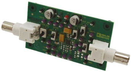
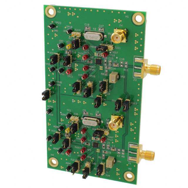
Data Sheet AD8436 AD8436 EVALUATION BOARD The AD8436-EVALZ provides a platform to evaluate AD8436 Table 6. performance. The board is fully assembled, tested, and ready to Switch Function use after connecting the power and signal sources. Figure 47 CORE_BUFFER Selects core or input buffer for the input is a photograph of the board and Figure 48 is the schematic. signal Signal connections are located on the primary and secondary INCOUP Selects ac or dc coupling to the core sides, with power and ground on the inner layers. Figure 42 to SDCOUT Selects the output buffer or the core Figure 46 illustrate the various design details of the board, output at the DCOUT BNC including basic layout and copper patterns. These figures are IBUF_VCC Enables or disables the input buffer useful references for application designs. OBUF_VCC Enables or disables the output buffer A Word About Using the AD8436 Evaluation Board Ample test points provide easy monitoring of inputs and The AD8436-EVALZ offers many options, without sacrificing outputs using standard test equipment. Unity is the input buffer simplicity. The board is tested and shipped with a 10 μF averaging default gain; for 2× gain, simply install a 0 Ω 0603 resistor (jumper) capacitor (CAVG), a 3.3 μF low-pass filter capacitor (CLPF), and a at Position R5. For higher IBUF gains, remove the 0 Ω resistor 0.1 μF capacitor to optimize crest factor (CCF) performance. To at Position RFBH (there is an internal 10 kΩ resistor from the evaluate minimum cost applications, remove both capacitors. The OBUF_OUT to IBUFIN−) and install a smaller value resistor in functions of the five switches are listed in Table 6. Position RFBL. A 100 Ω resistor establishes a gain of 100×. Single-Supply Operation Referring to Figure 48, single-supply operation requires the removal of Resistor R6. If needed, an optional capacitor in the range 0.1 μF to 4.7 μF may be installed in the R6 position for ambient noise decoupling (this is rarely required, however). Connect the negative supply pin (VEE) to ground (GND); otherwise, the negative supply rails remain open. Rev. E | Page 17 of 21
AD8436 Data Sheet 10033-142 10033-145 Figure 42. Assembly of the AD8436-EVALZ Figure 45. AD8436-EVALZ Power Plane 10033-143 10033-146 Figure 43. AD8436-EVALZ Primary Side Copper Figure 46. AD8436-EVALZ Ground Plane 10033-144 Figure 44. AD8436-EVALZ Secondary Side Copper Rev. E | Page 18 of 21
Data Sheet AD8436 10033-147 Figure 47. Photograph of the AD8436-EVALZ +V –V3 (RED) (GRN) GND1 GND2 GND3 GND4 GND5 GND6 CAVG C2 C13 10µF + CCF C4 TIBUFV+ +10µF 10µF TCAVG TCCF 0X.81RµF 0.1µF EN DIS 5–04V0°C TO + 5–04V0°C TO +125°C TSUM +125°C IBUF_VCC VEE 20 19 18 17 16 INCOUP SUM CAVG CCF VCC IBUFV+ VCC TOBUFV+ EN AC DC 1 DNC OBUFV+ 15 DIS CORE_BUF OBUF_VCC CORE CIN AC_IN 10µF TRMSIN TOBFOUT 2 14 RMS OBUFOUT + R8 BUF TIBUFOUT TOBUFIN− 0Ω 2.C2µ6F1 TACIN 3 IBUFOUT AD8436 OBUFIN– 13 TDCOUT RFBH4 BUF 0Ω DC C5 TIBFIN–4 12TOBUFIN+ OUT 0.47µF IBUFIN– OBUFIN+ CORE RFBL5 DNI TIBFIN+ TIGND C71 SDCOUT 1.5µF 5 11 IBUFIN+ IGND R1 BUF R31 10MΩ GAIN DNC OGND OUT VEE R72 8.06kΩ 6 7 8 9 10 0Ω TBUFGNR54 TOGND R2 TOUT C0.313µF R0Ω63 R04Ω1 0Ω 0Ω VEE CLPF 3.3µF 1OPTIONAL COMPONENTS TO CONFIGURE IBUFOUT AS A FILTER. 2REMOVE R7 FOR CORE-ONLY TESTS. 3FOR SINGLE SUPPLY OPERATION, REMOVE R6, SHORT OR REPLACE C3 WITH A 0Ω RESISTOR AND CONNECT THE SUPPLY GROUND OR RETURN TO 45TRTOHFBE CL GO IRNSE FUEIGSNEU TDRE ETS OTTH CLEOO FNOEFPTI G –IVNU.PRUET T BHUEF INFEPRU TF OBURF GFAEIRN FOOFR 2 G, IANISNT VAALLLU 0EΩS R >E2S×I.STOR AT R5 AND REMOVE RFBH. 10033-148 Figure 48. Evaluation Board Schematic Rev. E | Page 19 of 21
AD8436 Data Sheet OUTLINE DIMENSIONS DETAIL A (JEDEC 95) 4.10 0.30 4.00 SQ 0.25 PIN 1 3.90 0.18 INDICATOR PIN 1 0.50 16 20 I(NSEDEIC DAETTAOIRL AAR)EA OPTIONS BSC 15 1 2.75 EXPPAODSED 2.60 SQ 2.35 11 5 0.50 10 6 0.25 MIN TOP VIEW 0.40 BOTTOM VIEW 0.30 0.80 FOR PROPER CONNECTION OF 0.75 SIDE VIEW THE EXPOSED PAD, REFER TO 0.05 MAX THE PIN CONFIGURATION AND 0.70 0.02 NOM FUNCTION DESCRIPTIONS SECTION OF THIS DATA SHEET. COPLANARITY SEATING 0.08 PKG-005089 PLANE COMPLIANTTOJEDE0C.2 S0T RAENFDARDS MO-220-WGGD-11. 02-21-2017-B Figure 49. 20-Lead Lead Frame Chip Scale Package [LFCSP] 4 mm × 4 mm Body and 0.75 mm Package Height (CP-20-8) Dimensions shown in millimeters 0.345 (8.76) 0.341 (8.66) 0.337 (8.55) 20 11 0.158 (4.01) 0.154 (3.91) 0.150 (3.81) 0.244 (6.20) 1 10 0.236 (5.99) 0.228 (5.79) 0.010 (0.25) 0.020 (0.51) 0.065 (1.65) 0.069 (1.75) 0.006 (0.15) 0.010 (0.25) 0.049 (1.25) 0.053 (1.35) CO00P..00L10A04 N((00A..21R50I))TY 0.02B5S (C0.64) 0.012 (0.30) SPELAATNIENG 80°° 0.050 (1.27) 0R.E04F1 (1.04) 0.004 (0.10) 0.008 (0.20) 0.016 (0.41) COMPLIANTTO JEDEC STANDARDS MO-137-AD C(RINOEFNPETARRREOENNLCLTEIHN EOGSN EDLSIYM)AEANNRDSEI AORRNOESU NANORDEET DAIN-PO IPFNRFCO HINPECRSHI;A METEQIL UFLIOIVMRAE LUTEESNRET DISNI M FDOEERNSSIGIONN.S 09-12-2014-A Figure 50. 20-Lead Shrink Small Outline Package [QSOP] (RQ-20) Dimensions shown in inches and (millimeters) Rev. E | Page 20 of 21
Data Sheet AD8436 ORDERING GUIDE Model1 Temperature Range Package Description Package Option AD8436ACPZ-R7 −40°C to +125°C 20-Lead Lead Frame Chip Scale [LFCSP] CP-20-8 AD8436ACPZ-RL −40°C to +125°C 20-Lead Lead Frame Chip Scale [LFCSP] CP-20-8 AD8436ACPZ-WP −40°C to +125°C 20-Lead Lead Frame Chip Scale [LFCSP] CP-20-8 AD8436JCPZ-R7 0°C to +70°C 20-Lead Lead Frame Chip Scale [LFCSP] CP-20-8 AD8436JCPZ-RL 0°C to +70°C 20-Lead Lead Frame Chip Scale [LFCSP] CP-20-8 AD8436JCPZ-WP 0°C to +70°C 20-Lead Lead Frame Chip Scale [LFCSP] CP-20-8 AD8436ARQZ-R7 −40°C to +125°C 20-Lead Shrink Small Outline Package [QSOP] RQ-20 AD8436ARQZ-RL −40°C to +125°C 20-Lead Shrink Small Outline Package [QSOP] RQ-20 AD8436ARQZ −40°C to +125°C 20-Lead Shrink Small Outline Package [QSOP] RQ-20 AD8436BRQZ-R7 −40°C to +125°C 20-Lead Shrink Small Outline Package [QSOP] RQ-20 AD8436BRQZ-RL −40°C to +125°C 20-Lead Shrink Small Outline Package [QSOP] RQ-20 AD8436BRQZ −40°C to +125°C 20-Lead Shrink Small Outline Package [QSOP] RQ-20 AD8436-EVALZ Evaluation Board 1 Z = RoHS Compliant Part. ©2011–2017 Analog Devices, Inc. All rights reserved. Trademarks and registered trademarks are the property of their respective owners. D10033-0-3/17(E) Rev. E | Page 21 of 21
Mouser Electronics Authorized Distributor Click to View Pricing, Inventory, Delivery & Lifecycle Information: A nalog Devices Inc.: AD8436ACPZ-R7 AD8436ACPZ-RL AD8436ACPZ-WP AD8436ARQZ AD8436ARQZ-R7 AD8436ARQZ-RL AD8436BRQZ AD8436BRQZ-R7 AD8436BRQZ-RL AD8436-EVALZ AD8436JCPZ-R7 AD8436JCPZ-RL AD8436JCPZ-WP