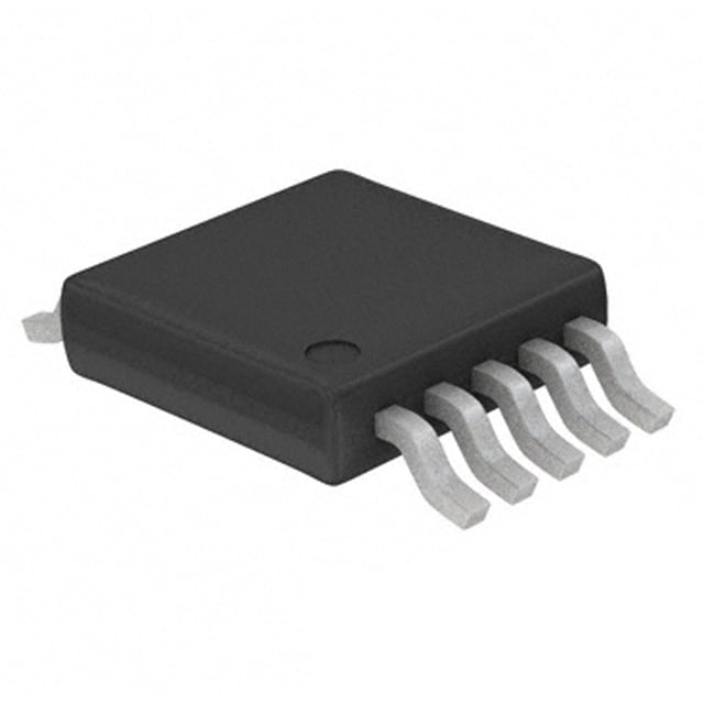
ICGOO在线商城 > 射频/IF 和 RFID > RF 放大器 > AD8351ARM
- 型号: AD8351ARM
- 制造商: Analog
- 库位|库存: xxxx|xxxx
- 要求:
| 数量阶梯 | 香港交货 | 国内含税 |
| +xxxx | $xxxx | ¥xxxx |
查看当月历史价格
查看今年历史价格
AD8351ARM产品简介:
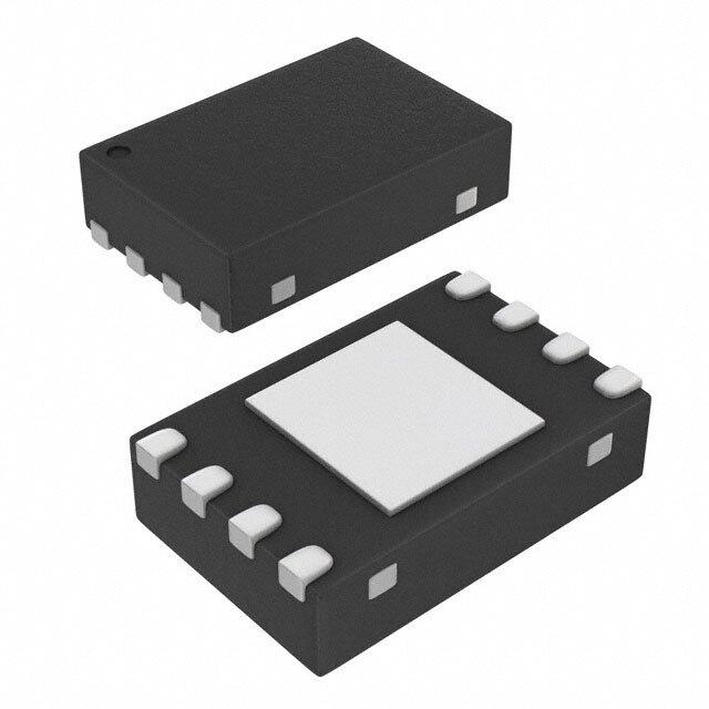
ICGOO电子元器件商城为您提供AD8351ARM由Analog设计生产,在icgoo商城现货销售,并且可以通过原厂、代理商等渠道进行代购。 AD8351ARM价格参考。AnalogAD8351ARM封装/规格:RF 放大器, 射频放大器 IC 通用 0Hz ~ 2.2GHz 10-MSOP。您可以下载AD8351ARM参考资料、Datasheet数据手册功能说明书,资料中有AD8351ARM 详细功能的应用电路图电压和使用方法及教程。
AD8351ARM是由Analog Devices Inc.生产的RF(射频)放大器,属于高性能、宽带宽的跨导放大器。其主要应用场景包括:

1. 无线通信系统:AD8351ARM广泛应用于基站收发信机、无线接入点和中继器等设备中。它能够处理宽带信号,支持多种无线通信标准(如GSM、CDMA、WCDMA、LTE等),适用于上变频和下变频链路中的增益控制。

2. 雷达与传感器系统:在雷达和传感器应用中,AD8351ARM可以作为驱动放大器或混频器的一部分,用于提高信号强度并改善系统的动态范围。其高线性度和低失真特性使其非常适合需要精确测量的应用场景。

3. 测试与测量设备:该器件也常用于矢量信号发生器、频谱分析仪和其他测试仪器中,提供可调增益功能以满足不同频率范围和功率水平的需求。

4. 光纤通信:在光纤通信领域,AD8351ARM可用作光电转换后的信号放大器,确保数据传输过程中信号质量不受损失。

5. 医疗电子:某些高端医疗成像设备可能使用此类RF放大器来增强接收信号的质量,从而获得更清晰的图像。

6. 卫星通信:由于其出色的性能参数,AD8351ARM还可用于卫星地面站设备中,负责信号的放大与处理。

总之,AD8351ARM凭借其卓越的电气特性和灵活性,在众多需要高频信号处理的场合中发挥着重要作用。
| 参数 | 数值 |
| 产品目录 | |
| 描述 | IC DIFF RF/IF AMP LOWDIST 10MSOP差分放大器 Low Distortion RF/IF IC |
| 产品分类 | |
| 品牌 | Analog Devices Inc |
| 产品手册 | |
| 产品图片 |
|
| rohs | 否不符合限制有害物质指令(RoHS)规范要求 |
| 产品系列 | 放大器 IC,差分放大器,Analog Devices AD8351ARM- |
| 数据手册 | |
| P1dB | 13.5dBm |
| 产品型号 | AD8351ARM |
| PCN设计/规格 | |
| RF类型 | 通用 |
| 产品种类 | 差分放大器 |
| 供应商器件封装 | 10-MSOP |
| 共模抑制比—最小值 | 43 dB |
| 包装 | 管件 |
| 商标 | Analog Devices |
| 噪声系数 | - |
| 增益 | 26dB |
| 安装风格 | SMD/SMT |
| 封装 | Tube |
| 封装/外壳 | 10-TFSOP,10-MSOP(0.118",3.00mm 宽) |
| 封装/箱体 | MSOP-10 |
| 工作电源电压 | 3 V to 5.5 V |
| 工厂包装数量 | 50 |
| 带宽 | 2.2 GHz |
| 最大功率耗散 | 320 mW |
| 最大工作温度 | + 85 C |
| 最大输入电阻 | 5 kOhms |
| 最小工作温度 | - 40 C |
| 标准包装 | 50 |
| 测试频率 | 10MHz |
| 电压-电源 | 3 V ~ 5.5 V |
| 电流-电源 | 28mA ~ 32mA |
| 电源电流 | 28 mA |
| 稳定时间 | 3 ns |
| 系列 | AD8351 |
| 视频文件 | http://www.digikey.cn/classic/video.aspx?PlayerID=1364138032001&width=640&height=505&videoID=2245193150001 |
| 转换速度 | 13000 V/us |
| 通道数量 | 1 Channel |
| 频率 | 0Hz ~ 2.2GHz |






- 商务部:美国ITC正式对集成电路等产品启动337调查
- 曝三星4nm工艺存在良率问题 高通将骁龙8 Gen1或转产台积电
- 太阳诱电将投资9.5亿元在常州建新厂生产MLCC 预计2023年完工
- 英特尔发布欧洲新工厂建设计划 深化IDM 2.0 战略
- 台积电先进制程称霸业界 有大客户加持明年业绩稳了
- 达到5530亿美元!SIA预计今年全球半导体销售额将创下新高
- 英特尔拟将自动驾驶子公司Mobileye上市 估值或超500亿美元
- 三星加码芯片和SET,合并消费电子和移动部门,撤换高东真等 CEO
- 三星电子宣布重大人事变动 还合并消费电子和移动部门
- 海关总署:前11个月进口集成电路产品价值2.52万亿元 增长14.8%


PDF Datasheet 数据手册内容提取
Low Distortion Differential RF/IF Amplifier Data Sheet AD8351 FEATURES FUNCTIONAL BLOCK DIAGRAM −3 dB bandwidth of 2.2 GHz for A = 12 dB V AD8351 Single resistor programmable gain: 0 dB ≤ AV ≤ 26 dB VOCM PWUP BIAS CELL Differential interface VPOS Low noise input stage 2.7 nV/√Hz at A = 10 dB V RGP1 Low harmonic distortion −79 dBc second at 70 MHz INHI OPHI −81 dBc third at 70 MHz INLO OPLO OIP3 of 31 dBm at 70 MHz COMM Single-supply operation: 3 V to 5.5 V RGP2 Low power dissipation: 28 mA at 5 V AFSaldesjwtu s sretaatttbelil noe gfo 1 ua3nt,pd0u0 ot0v c Veor/mdμrsmi voen r-emcoovdeer vyo ltage ––21000 AGAAEDDANN86ICAN36OL54 DO15RR GEW(IR V =IILNTI N 8HP=G0 U M11 TT0kH HdΩ=zBE )7 O0MFHz 20IR0NΩGHI AD8351100nF25Ω A1D4-6B6I4T5 Power-down capability –30 SFHUNDNR2 D == =–6 79–8.11..5d1dBdBBcFS INLO 100nF25Ω ADC –40 HD3 = –80.7dBc THD = –75.9dBc APPLICATIONS –50 SFDR = 78.2dBc –60 Differential ADC drivers –70 Single-ended-to-differential conversion –80 2 3 IF sampling receivers –90 + RF/IF gain blocks –100 SAW filter interfacing –110 ––113200 03145-001 Figure 1. GENERAL DESCRIPTION The AD8351 is a low cost differential amplifier useful in RF and differential configuration. The exceptionally good distortion IF applications up to 2.2 GHz. The voltage gain can be set from performance makes the AD8351 an ideal solution for 12-bit and unity to 26 dB using a single external gain resistor. The AD8351 14-bit IF sampling receiver designs. provides a nominal 150 Ω differential output impedance. The Fabricated in Analog Devices, Inc., high speed XFCB process, excellent distortion performance and low noise characteristics the AD8351 has high bandwidth that provides high frequency of this device allow for a wide range of applications. performance and low distortion. The quiescent current of the The AD8351 is designed to satisfy the demanding performance AD8351 is 28 mA typically. The AD8351 amplifier comes in a requirements of communications transceiver applications. The compact 10-lead MSOP package or in a 16-lead LFCSP package, device can be used as a general-purpose gain block, an ADC and operates over the temperature range of −40°C to +85°C. driver, and a high speed data interface driver, among other functions. The AD8351 can also be used as a single-ended-to- differential amplifier with similar distortion products as in the Rev. D Document Feedback Information furnished by Analog Devices is believed to be accurate and reliable. However, no responsibility is assumed by Analog Devices for its use, nor for any infringements of patents or other One Technology Way, P.O. Box 9106, Norwood, MA 02062-9106, U.S.A. rights of third parties that may result from its use. Specifications subject to change without notice. No license is granted by implication or otherwise under any patent or patent rights of Analog Devices. Tel: 781.329.4700 ©2003–2015 Analog Devices, Inc. All rights reserved. Trademarks and registered trademarks are the property of their respective owners. Technical Support www.analog.com
AD8351 Data Sheet TABLE OF CONTENTS Features .............................................................................................. 1 Gain Adjustment ........................................................................ 12 Applications ....................................................................................... 1 Common-Mode Adjustment .................................................... 12 Functional Block Diagram .............................................................. 1 Input and Output Matching ...................................................... 12 General Description ......................................................................... 1 Single-Ended-to-Differential Operation ................................. 13 Revision History ............................................................................... 2 ADC Driving ............................................................................... 13 Specifications ..................................................................................... 3 Analog Multiplexing .................................................................. 14 Absolute Maximum Ratings ............................................................ 5 I/O Capacitive Loading ............................................................. 14 ESD Caution .................................................................................. 5 Transmission Line Effects ......................................................... 15 Pin Configurations and Function Descriptions ........................... 6 Characterization Setup .............................................................. 16 Typical Performance Characteristics ............................................. 7 Evaluation Board ............................................................................ 17 Theory of Operation ...................................................................... 12 Outline Dimensions ....................................................................... 19 Basic Concepts ............................................................................ 12 Ordering Guide ............................................................................... 19 REVISION HISTORY 1/15—Rev. C to Rev. D Changes to Noise Distortion Parameter, Table 1 .......................... 3 Changes to Ordering Guide .......................................................... 19 3/14—Rev. B to Rev. C Updated Format .................................................................. Universal Added 16-Lead LFCSP Package................................... Throughout Changes to Features .......................................................................... 1 Changes to Table 3 and Added Figure 3; Renumbered Sequentially ....................................................................................... 6 Updated Outline Dimensions; Added Figure 52 ........................ 19 Moved, Changes to Ordering Guide ............................................ 19 2/04—Rev. A to Rev. B Changes to Ordering Guide ............................................................ 4 Changes to TPC 4 ............................................................................. 5 3/03—Rev. 0 to Rev. A Changes to Ordering Guide ............................................................ 4 Change to Table 3 ........................................................................... 15 3/03—Revision 0: Initial Version Rev. D | Page 2 of 19
Data Sheet AD8351 SPECIFICATIONS V = 5 V, R = 150 Ω, R = 110 Ω (A = 10 dB), f = 70 MHz, T = 25°C, parameters specified differentially, unless otherwise noted. S L G V Table 1. Parameter Test Conditions/Comments Min Typ Max Unit DYNAMIC PERFORMANCE −3 dB Bandwidth GAIN = 6 dB, V ≤ 1.0 V p-p 3,000 MHz OUT GAIN = 12 dB, V ≤ 1.0 V p-p 2,200 MHz OUT GAIN = 18 dB, V ≤ 1.0 V p-p 600 MHz OUT Bandwidth for 0.1 dB Flatness 0 dB ≤ GAIN ≤ 20 dB, V ≤ 1.0 V p-p 200 MHz OUT Bandwidth for 0.2 dB Flatness 0 dB ≤ GAIN ≤ 20 dB, V ≤ 1.0 V p-p 400 MHz OUT Gain Accuracy Using 1% resistor for R , 0 dB ≤ A ≤ 20 dB ±1 dB G V Gain Supply Sensitivity V ± 5% 0.08 dB/V S Gain Temperature Sensitivity −40°C to +85°C 3.9 mdB/°C Slew Rate R = 1 kΩ, V = 2 V step 13,000 V/μs L OUT R = 150 Ω, V = 2 V step 7,500 V/μs L S Settling Time 1 V step to 1% <3 ns Overdrive Recovery Time V = 4 V to 0 V step, V ≤ ±10 mV <2 ns IN OUT Reverse Isolation (S12) −67 dB INPUT/OUTPUT CHARACTERISTICS Input Common-Mode Voltage Adjustment Range 1.2 to 3.8 V Max Output Voltage Swing 1 dB compressed 4.75 V p-p Output Common-Mode Offset 40 mV Output Common-Mode Drift −40°C to +85°C 0.24 mV/°C Output Differential Offset Voltage 20 mV Output Differential Offset Drift −40°C to +85°C 0.13 mV/°C Input Bias Current ±15 μA Input Resistance1 5 kΩ Input Capacitance1 0.8 pF CMRR 43 dB Output Resistance1 150 Ω Output Capacitance1 0.8 pF POWER INTERFACE Supply Voltage 3 5.5 V PWUP Threshold 1.3 V PWUP Input Bias Current PWUP at 5 V 100 μA PWUP at 0 V 25 μA Quiescent Current 28 32 mA NOISE/DISTORTION 10 MHz Second/Third Harmonic Distortion2 R = 1 kΩ, V = 2 V p-p −95/−93 dBc L OUT R = 150 Ω, V = 2 V p-p −80/−69 dBc L OUT Third-Order IMD R = 1 kΩ, f1 = 9.5 MHz, f2 = 10.5 MHz, −90 dBc L V = 2 V p-p composite OUT R = 150 Ω, f1 = 9.5 MHz, f2 = 10.5 MHz, −70 dBc L V = 2 V p-p composite OUT Output Third-Order Intercept f1 = 9.5 MHz, f2 = 10.5 MHz 33 dBm Noise Spectral Density (RTI) 2.65 nV/√Hz 1 dB Compression Point 13.5 dBm Rev. D | Page 3 of 19
AD8351 Data Sheet Parameter Test Conditions/Comments Min Typ Max Unit 70 MHz Second/Third Harmonic Distortion2 R = 1 kΩ, V = 2 V p-p −79/−81 dBc L OUT R = 150 Ω, V = 2 V p-p −65/−66 dBc L OUT Third-Order IMD R = 1 kΩ, f1 = 69.5 MHz, f2 = 70.5 MHz, −85 dBc L V = 2 V p-p composite OUT R = 150 Ω, f1 = 69.5 MHz, f2 = 70.5 MHz, −69 dBc L V = 2 V p-p composite OUT Output Third-Order Intercept f1 = 69.5 MHz, f2 = 70.5 MHz 31 dBm Noise Spectral Density (RTI) 2.70 nV/√Hz 1 dB Compression Point 13.3 dBm 140 MHz Second/Third Harmonic Distortion2 R = 1 kΩ, V = 2 V p-p −69/−69 dBc L OUT R = 150 Ω, V = 2 V p-p −54/−53 dBc L OUT Third-Order IMD R = 1 kΩ, f1 = 139.5 MHz, f2 = 140.5 MHz, −79 dBc L V = 2 V p-p composite OUT R = 150 Ω, f1 = 139.5 MHz, f2 = 140.5 MHz, −67 dBc L V = 2 V p-p composite OUT Output Third-Order Intercept f1 = 139.5 MHz, f2 = 140.5 MHz 29 dBm Noise Spectral Density (RTI) 2.75 nV/√Hz 1 dB Compression Point 13 dBm 240 MHz Second/Third Harmonic Distortion2 R = 1 kΩ, V = 2 V p-p −60/−66 dBc L OUT R = 150 Ω, V = 2 V p-p −46/−50 dBc L OUT Third-Order IMD R = 1 kΩ, f1 = 239.5 MHz, f2 = 240.5 MHz, −76 dBc L V = 2 V p-p composite OUT R = 150 Ω, f1 = 239.5 MHz, f2 = 240.5 MHz, −62 dBc L V = 2 V p-p composite OUT Output Third-Order Intercept f1 = 239.5 MHz, f2 = 240.5 MHz 27 dBm Noise Spectral Density (RTI) 2.90 nV/√Hz 1 dB Compression Point 13 dBm 1 Values are specified differentially. 2 See the Single-Ended-to-Differential Operation section for single-ended-to-differential performance. Rev. D | Page 4 of 19
Data Sheet AD8351 ABSOLUTE MAXIMUM RATINGS ESD CAUTION Table 2. Parameter Rating Supply Voltage VPOS 6 V PWUP Voltage VPOS Internal Power Dissipation 320 mW θ 125°C/W JA Maximum Junction Temperature 125°C Operating Temperature Range −40°C to +85°C Storage Temperature Range −65°C to +150°C Lead Temperature Range (Soldering 60 sec) 300°C Stresses at or above those listed under Absolute Maximum Ratings may cause permanent damage to the product. This is a stress rating only; functional operation of the product at these or any other conditions above those indicated in the operational section of this specification is not implied. Operation beyond the maximum operating conditions for extended periods may affect product reliability. Rev. D | Page 5 of 19
AD8351 Data Sheet PIN CONFIGURATIONS AND FUNCTION DESCRIPTIONS P M PWUP 1 10 VOCM WU C C OC P N N V RGP1 2 AD8351 9 VPOS 6 5 4 3 INHI 3 TOP VIEW 8 OPHI 1 1 1 1 RINGLPO2 45 (Not to Scale) 76 OCOPLMOM 03145-050 RGINPH1I 12 AD8351 1112 OVPPOHSI TOP VIEW INLO 3 (Not to Scale) 10 OPLO RGP2 4 9 COMM 5 6 7 8 C C C C N N N N NOTES 1.NC = NO CONNECT. DO NOT CONNECT TO THIS PIN. 2.GITMHNPEDE EDAXANPNDOC MSEEU GDSR TP OBAUEDN SIDSO PILNLDTAEENRREEN.DA LTLOY A C LOONWNECTED TO 03145-002 Figure 2. 10-Lead MSOP Pin Configuration Figure 3. 16-Lead LFCSP Pin Configuration Table 3. Pin Function Descriptions Pin No. 10-Lead MSOP 16-Lead LFCSP Mnemonic Description 1 16 PWUP Apply a positive voltage (1.3 V ≤ V ≤ VPOS) to activate device. PWUP 2 1 RGP1 Gain Resistor Input 1. 3 2 INHI Balanced Differential Input. Biased to midsupply, typically ac-coupled. 4 3 INLO Balanced Differential Input. Biased to midsupply, typically ac-coupled. 5 4 RGP2 Gain Resistor Input 2. 6 9 COMM Device Common. Connect to low impedance ground. 7 10 OPLO Balanced Differential Output. Biased to VOCM, typically ac-coupled. 8 11 OPHI Balanced Differential Output. Biased to VOCM, typically ac-coupled. 9 12 VPOS Positive Supply Voltage. 3 V to 5.5 V. 10 13 VOCM Voltage applied to this pin sets the common-mode voltage at both the input and output. Typically decoupled to ground with a 0.1 μF capacitor. 5, 6, 7, 8, 14, 15 NC No connect. Do not connect to this pin. EPAD Exposed Pad. The exposed pad is internally connected to GND and must be soldered to a low impedance ground plane. Rev. D | Page 6 of 19
Data Sheet AD8351 TYPICAL PERFORMANCE CHARACTERISTICS V = 5 V, T = 25°C, unless otherwise noted. S 20 30 RG = 20Ω RG = 10Ω 25 15 RG = 80Ω 20 dB) 10 dB) RG = 50Ω AIN ( RG = 200Ω AIN ( 15 G 5 G 10 RG = 200Ω 0 5 –5 0 1 10 FREQUE1N0C0Y (MHz) 1000 10000 03145-003 1 10 FREQUE1N0C0Y (MHz) 1000 10000 03145-006 Figure 4. Gain vs. Frequency for a 150 Ω Differential Load Figure 7. Gain vs. Frequency for a 1 kΩ Differential Load (AV = 6 dB, 12 dB, and 18 dB) (AV = 10 dB, 18 dB, and 26 dB) 35 1.0 0.9 30 0.8 0.7 0.6 25 0.5 20 dB) 00..43 N (dB) 15 TNESS ( 00..210 RL = 150Ω GAI 105 RL = OPEN AIN FLA–––000...231 RL = 1kΩ RL = 150Ω G––00..45 0 –0.6 –0.7 –5 RL = 1kΩ –0.8 –0.9 –10 –1.0 10 100 RG (Ω) 1k 10k 03145-004 1 10FREQUENCY (MHz1)00 1000 03145-007 Figure 5. Gain vs. Gain Resistor, RG (f = 100 MHz, Figure 8. Gain Flatness vs. Frequency RL = 150 Ω, 1 kΩ, and Open) (RL = 150 Ω and 1 kΩ, AV = 10 dB) 10.75 10.50 0 –10 10.50 10.25 –20 GAIN; R = 1kΩ (dB)L11009...027055 991..057.0500 = 150Ω (dB)GAIN; RL ISOLATION (dB)––––65430000 –70 9.50 9.25 –80 9.25 9.00 –90 –50 –30 –10 T1E0MPERA30TURE (5°0C) 70 90 110 03145-005 0 100 200 300 FR4E00QUE5N00CY (6M0H0z) 700 800 900 1000 03145-008 Figure 6. Gain vs. Temperature at 100 MHz (AV = 10 dB Figure 9. Isolation vs. Frequency (AV = 10 dB) Rev. D | Page 7 of 19
AD8351 Data Sheet –30 –45 –50 SINGLE-ENDED INPUT c) c) –55 B B d –40 HD3 –55 d OS = 5V ( –50 –65 OS = 3V ( N (dBc) ––6605 P HD2 P O V V TI –70 N; –60 HD2 –75 N; OR STORTIO –70 HD3 –85 STORTIO NIC DIST ––7850 HD2 NIC DI –80 DIFFERENTIAL INPUT –95 NIC DI ARMO –85 HD3 O O H –90 M M R –90 –105 R A A –95 H H –1000 25 50 75 FR1E00QUE1N2C5Y (1M5H0z) 175 200 225 250–115 03145-009 –1000 10 20 30 FR4E0QUE5N0CY (M60Hz) 70 80 90 100 03145-012 Figure 10. Harmonic Distortion vs. Frequency for 2 V p-p into RL = 1 kΩ Figure 13. Harmonic Distortion vs. Frequency for 2 V p-p into RL = 1 kΩ Using (AV = 10 dB, at 3 V and 5 V Supplies) Single-Ended Input (AV = 10 dB) 0 –20 –50 SINGLE-ENDED INPUT dBc) –10 HD3 –30 dBc) –55 POS = 5V ( ––3200 ––5400 POS = 3V ( ON (dBc) ––6605 HD3 N; V –40 HD2 –60 N; V ORTI –70 RTIO –50 –70 RTIO DIST –75 STO STO NIC –80 HD2 ONIC DI ––7600 HD3 DIFFERENTIAL INPUT ––9800 ONIC DI HARMO ––8950 M M R R A –80 HD2 –100 A –95 H H –900 25 50 75 FR1E00QUE1N2C5Y (1M5H0z) 175 200 225 250–110 03145-010 –1000 10 20 30 FR4E0QUE5N0CY (M60Hz) 70 80 90 100 03145-013 Figure 11. Harmonic Distortion vs. Frequency for 2 V p-p into RL = 150 Ω Figure 14. Harmonic Distortion vs. Frequency for 2 V p-p into RL = 150 Ω (AV = 10 dB) Using Single-Ended Input (AV = 10 dB) 3.00 3.00 2.95 2.95 OISE SPECTRAL DENSITY (nV/√Hz) 2222222.......66778890505050 OISE SPECTRAL DENSITY (nV/√Hz) 2222222.......66778890505050 N N 2.55 2.55 2.500 50 FR1E00QUENCY (1M5H0z) 200 250 03145-011 2.500 50 FR1E00QUENCY (1M5H0z) 200 250 03145-014 Figure 15. Noise Spectral Density (RTI) vs. Frequency Figure 12. Noise Spectral Density (RTI) vs. Frequency (RL = 150 Ω, 5 V Supply, AV = 10 dB) (RL = 150 Ω, 3 V Supply, AV = 10 dB) Rev. D | Page 8 of 19
Data Sheet AD8351 16 –70 14 m) B –75 ESSION (d 1120 RVRPLL O== S11 5k=0Ω 5ΩV MD (dBc) –80 PR R I M 8 E CO RL = 150Ω RD 1dB 6 VRPL O= S1 k=Ω 3V RD-O –85 PUT 4 THI UT –90 O 2 0 –95 0 25 50 75 FR10E0QUE1N25CY (1M5H0z) 175 200 225 250 03145-015 0 25 50 75 FR10E0QUE1N25CY (1M5H0z) 175 200 225 250 03145-018 Figure 16. Output Compression Point, P1 dB, vs. Frequency Figure 19. Third-Order Intermodulation Distortion vs. Frequency for a 2 V p-p (RL = 150 Ω and 1 kΩ, AV = 10 dB, at 3 V and 5 V Supplies) Composite Signal into RL = 1 kΩ (AV = 10 dB, at 5 V Supplies) 16 –50 14 VPOS = 5V m) B –55 ESSION (d 1120 MD (dBc) –60 PR R I OM 8 VPOS = 3V DE C R dB 6 D-O –65 1 R PUT 4 THI UT –70 O 2 0 –75 10 GAIN RE1S0I0STOR (Ω) 1000 03145-016 0 25 50 75 FR10E0QUE1N25CY (1M5H0z) 175 200 225 250 03145-019 Figure 17. Output Compression Point, P1 dB, vs. RG (f =100 MHz, Figure 20. Third-Order Intermodulation Distortion vs. Frequency for a 2 V p-p RL = 150 Ω, AV = 10 dB, at 3 V and 5 V Supplies) Composite Signal into RL = 150 Ω (AV = 10 dB, at 5 V Supplies) 13.29 13.30 13.31 O13.32UTPU13.33T 1d13.34B CO13.35MPR13.36ESS13.37ION (13.38dB) 13.39 13.40 13.41 03145-017 –68.T0H–IR68D.2-O–R68D.4ER– 6I8N.6TE–R68M.8OD–6U9L.0AT–6IO9.N2 D–6IS9.T4O–R69T.I6ON–6 9(d.8Bc–)70.0 03145-020 Figure 18. Output Compression Point Distribution Figure 21. Third-Order Intermodulation Distortion Distribution (f = 70 MHz, RL = 150 Ω, AV = 10 dB) (f = 70 MHz, RL = 150 Ω, AV = 10 dB) Rev. D | Page 9 of 19
AD8351 Data Sheet 4000 0 3500 Ω) 3000 –25 E ( D DANCE MAGNITU 221505000000 –50 PHASE (Degrees) 3GHz 10MHz 10MHz E MP 1000 –75 500MHz I 3GHz WITH 50Ω 500MHz 500 TERMINATIONS 0 –100 WITHOUT 10 FREQUE1N0C0Y (MHz) 1000 03145-021 TERMINATIONS 03145-024 Figure 22. Input Impedance vs. Frequency Figure 25. Input Reflection Coefficient vs. Frequency (RS = RL = 100 Ω With and Without 50 Ω Terminations) 160 30 150 25 UDE (Ω) 140 20 Degrees) NIT E ( G S MPEDANCE MA 113200 1150 MPEDANCE PHA 105M00HMzHz I 110 5 I 100 0 3GHz 10 FREQUE1N0C0Y (MHz) 1000 03145-022 03145-025 Figure 23. Output Impedance vs. Frequency Figure 26. Output Reflection Coefficient vs. Frequency (RS = RL = 100 Ω) 0 20 19 –2 18 17 –4 16 15 grees) ––68 111234 AY (ps) De 11 EL PHASE ( ––1102 78910 GROUP D 6 –14 5 4 –16 3 1 –18 0 0 25 50 75 FR1E00QUE1N2C5Y (1M5H0z) 175 200 225 250 03145-023 Figure 24. Phase and Group Delay (AV = 10 dB, at 5 V Supplies) Rev. D | Page 10 of 19
Data Sheet AD8351 80 3 VOUT 70 2 RL = 150Ω 60 1 dB) E (V) VIN RR ( 50 RL = 1kΩ TAG 0 M L C O V 40 –1 30 –2 201 10FREQUENCY (MHz1)00 1000 03145-026 –30 5 10 15 20TIM2E5 (ns)30 35 40 45 50 03145-029 Figure 27. Common-Mode Rejection Ratio, CMRR (RS = 100 Ω) Figure 30. Overdrive Recovery Using Sinusoidal Input Waveform RL = 150 Ω (AV = 10 dB, at 5 V Supplies) 0.6 1.00 0pF 0.75 0.4 5pF 2pF 0.50 10pF 0.2 V) V) 0.25 E ( E ( AG 0 AG 0 T T L L O O V V–0.25 –0.2 –0.50 –0.4 –0.75 –0.6 –1.00 15 16 17 18 19TIM2E0 (ns)21 22 23 24 25 03145-027 0 0.5 1.0 1.5 TIM2E.0 (ns) 2.5 3.0 3.5 4.0 03145-030 Figure 28. Transient Response Under Capacitive Loading Figure 31. Large Signal Transient Response for a 1 V p-p Output Step (RL = 150 Ω, CL = 0 pF, 2 pF, 5 pF, 10 pF) (AV = 10 dB, RIP = 25 Ω) 5.0 5 4.5 4 4.0 3 3.5 2 PUT (V) 32..05 LING (%) 01 OUT 2.0 ETT –1 S 1.5 –2 1.0 –3 0.5 –4 0 –5 0 5 10 15 TIM2E0 (ns) 25 30 35 40 03145-028 0 3 6TIME (ns)9 12 15 03145-031 Figure 29. 2× Output Overdrive Recovery (RL = 150 Ω, AV = 10 dB) Figure 32. 1% Settling Time for a 2 V p-p Step (AV = 10 dB, RL = 150 Ω) Rev. D | Page 11 of 19
AD8351 Data Sheet THEORY OF OPERATION BASIC CONCEPTS Table 4. Gain Resistor Selection for Common Gain Values Differential signaling is used in high performance signal chains, (Load Resistance Is Specified as Single-Ended) where distortion performance, signal-to-noise ratio, and low Gain, A R (R = 75 Ω) R (R = 500 Ω) V G L G L power consumption is critical. Differential circuits inherently 0 dB 680 Ω 2 kΩ provide improved common-mode rejection and harmonic 6 dB 200 Ω 470 Ω distortion performance as well as better immunity to 10 dB 100 Ω 200 Ω interference and ground noise. 20 dB 22 Ω 43 Ω UP CM COMMON-MODE ADJUSTMENT W C C O P N N V 16 15 14 13 The output common-mode voltage level is the dc offset voltage RGP1 present at each of the differential outputs. The ac signals are of 1 VPOS 12 equal amplitude with a 180° phase difference but are centered at INHI OPHI A BALANCED 2 11 the same common-mode voltage level. The common-mode output SOURCE RG INLO OPLO RL 2A voltage level can be adjusted from 1.2 V to 3.8 V by driving the 3 10 A desired voltage level into the VOCM pin, as illustrated in Figure 34. RGP2 4 COMM 9 NC16 NC15 NC14 NC13 03145-032 PWUP16 NC15 NC14 VOCM13 C0.D1EµCFL 1TVV.OOS2CVM Figure 33. Differential Circuit Representation 3.8V RGP1 0.1µF Figure 33 illustrates the expected input and output waveforms 1 VPOS 12 for a typical application. Usually the applied input waveform is a INHI OPHI BALANCED 2 11 balanced differential drive, where the signal applied to the INHI SOURCE RG INLO OPLO RL and INLO pins are equal in amplitude and differ in phase by 180°. 3 10 In some applications, baluns may be used to transform a single- RGP2 4 COMM 9 ended drive signal to a differential signal. The AD8351 may also be used to transform a single-ended signal to a differential signal. NC5 NC6 NC7 NC8 03145-033 GAIN ADJUSTMENT Figure 34. Common-Mode Adjustment The differential gain of the AD8351 is set using a single external INPUT AND OUTPUT MATCHING resistor, RG, which is connected between the RGP1 pin and the The AD8351 provides a moderately high differential input imped- RGP2 pin. The gain can be set to any value between 0 dB and 26 dB ance of 5 kΩ. In practical applications, the input of the AD8351 using the resistor values specified in Figure 5, with common gain is terminated to a lower impedance to provide an impedance values provided in Table 4. The board traces used to connect the match to the driving source, as shown in Figure 35. Place the external gain resistor must be balanced and as short as possible to terminating resistor, R , as close as possible to the input pins to T help prevent noise pickup and to ensure balanced gain and stability. minimize reflections due to impedance mismatch. The 150 Ω The low frequency voltage gain of the AD8351 can be modeled as output impedance may need to be transformed to provide the desired output match to a given load. Matching components R R (5.6)9.2R R V A L G F L OUT can be calculated using a Smith chart or by using a resonant V R R 4.619.5R R R 39R V G L G L F G IN approach to determine the matching network that results in a where: complex conjugate match. The input and output impedances R is 350 Ω (internal). and reflection coefficients are provided in Figure 22, Figure 23, F R is the single-ended load resistance. Figure 24, and Figure 25. For additional information on reactive L R is the gain setting resistor. matching to differential sources and loads, refer to the Applications G section of the AD8350 data sheet. VPOS RS RT 0.1µF 0.1µF 27LnSF 190MHz SAW BALANCED SOURCE RS = RT RG AD8351 150Ω C8pPF 50Ω RS RT 0.1µF 0.1µF 27LnSF 03145-034 Figure 35. Example of Differential SAW Filter Interface (fC = 190 MHz) Rev. D | Page 12 of 19
Data Sheet AD8351 Figure 35 illustrates a surface acoustic wave (SAW) filter interface. 35 Many SAW filters are inherently differential, allowing for a low 30 loss output match. In this example, the SAW filter requires a 50 Ω source impedance to provide the desired center frequency and RL = 1000Ω 25 Q. The series L shunt C output network provides a 150 Ω to 50 Ω impedance transformation at the desired frequency of B) 20 d oSmpeirtaht icohna.r Tt ihne Fimigupreed 3a6n.c e transformation is illustrated on a GAIN ( 15 RL = 150Ω RL = 500Ω It is possible to drive a single-ended SAW filter by connecting 10 the unused output to ground using the appropriate terminating resistance. The overall gain of the system is reduced by 6 dB 5 because only half of the signal is available to the input of the 0 SAW filter. 50 10 RG10 (0Ω) 1000 03145-037 Figure 38. Gain Selection 25 100 7 6 RL = 1000Ω 10 200 5 500 Ω) 4 50Ω 150Ω 500 0 R (kF 3 RL = 500Ω 200 SHUNT C SERIES L 100 2 50 1 25 RL = 150Ω 0 10 03145-035 10 RG10 (0Ω) 1000 03145-038 Figure 36. Smith Chart Representation of SAW Filter Output Matching Network Figure 39. Feedback Resistor Selection 0.1µF 0.1µF ADC DRIVING 50Ω 50Ω RG AD8351 0.1µF RL The circuit in Figure 40 represents a simplified front end of the AD8351 driving the AD6645, which is a 14-bit, 105 MSPS ADC. 0.1µF For optimum performance, the AD6645 and the AD8351 are 25Ω RF 03145-036 ddrififveerne ndtiifafle rinenptuiat lilmy. pTehdea rnecseis ttoor tsh Re 1s oaunrdc eR 2w pitrhe sRe3n ta an d50 R Ω4 Figure 37. Single-Ended Application providing isolation from the analog-to-digital input. The gain SINGLE-ENDED-TO-DIFFERENTIAL OPERATION setting resistor for the AD8351 is R . The AD6645 presents a G The AD8351 can easily be configured as a single-ended-to- 1 kΩ differential load to the AD8351 and requires a 2.2 V p-p differential gain block, as illustrated in Figure 37. The input signal differential signal between AIN and AIN for a full-scale output. is ac-coupled and applied to the INHI input. The unused input This AD8351 circuit then provides the gain, isolation, and source is ac-coupled to ground. Select the values of C1 through C4 such matching for the AD6645. The AD8351 also provides a balanced that their reactances are negligible at the desired frequency of input, not provided by the balun, to the AD6645, which is essential operation. To balance the outputs, an external feedback resistor, for second-order cancellation. The signal generator is bipolar, R, is required. To select the gain resistor and the feedback resistor, centered around ground. Connecting the VOCM pin (Pin 10 on F refer to Figure 38 and Figure 39. From Figure 38, select an R for the MSOP and Pin 13 on the LFCSP) of the AD8351 to the VREF G the required dB gain at a given load. Next, select from Figure 39 pin of the AD6645 sets the common-mode output voltage of the an R resistor for the selected R and load. AD8351 at 2.4 V. This voltage is bypassed with a 0.1 μF capacitor. F G Increasing the gain of the AD8351 increases the system noise and Even though the differential balance is not perfect under these thus decrease the SNR but does not significantly affect the conditions, the distortion performance is still impressive. Figure 13 distortion. The circuit in Figure 40 can provide SFDR performance and Figure 14 show the second and third harmonic distortion of better than −90 dBc with a 10 MHz input and −80 dBc with a performance when driving the input of the AD8351 using a 70 MHz input at a gain of 10 dB. single-ended 50 Ω source. Rev. D | Page 13 of 19
AD8351 Data Sheet 100nF N-BIT 25Ω INHI OPHI 25Ω AIN BIT 1 DINIGTEITRAFLACE BALAN5C0ΩE RG AD8351 AD6645 INHI PWOUPPHI SOURCE 251Ω00nFINLO VOCOMPLO25Ω AINVREF DIOGUITTAL ISNIGPUNTA L1 RG RGP1 AD8351 03145-039 RINGLPO2 OPLO Figure 40. ADC Driving Application Using Differential Input BIT 2 The circuit of Figure 41 represents a single-ended input to PWUP differential output configuration of the AD8351 driving the INHI OPHI AD6645. In this case, R1 provides the input impedance. R is RGP1 the gain setting resistor. The resistor RF is required to balanGce ISNIGPUNTA L2 RG RGP2 AD8351 MOLOUUATXPDUT the output voltages required for second-order cancellation by INLO OPLO the AD6645 and can be selected using a chart (see the Single- Ended-to-Differential Operation section). The circuit depicted in Figure 41 can provide SFDR performance of better than −90 dBc with a 10 MHz input and −77 dBc with a 70 MHz input. BIT N RF PWUP INHI 100nF OPHI INHI R1 OPHI 25Ω AIN SIGNAL RGP1 SSOEINNUGDR5LEC0EΩDE- 25Ω RINGLO AD8351OPLO25Ω AAIND6V6R4E5F DIOGUITTAL INPUT N RG RINGLPO2 AD83O5P1LO 03145-041 25Ω 100nF VOCM Figure 42. Using Several AD8351s to Form an N-Channel Analog MUX 100nF 03145-040 I/O CAPACITIVE LOADING Figure 41. ADC Driving Application Using Single-Ended Input Input or output direct capacitive loading greater than a few ANALOG MULTIPLEXING picofarads can result in excessive peaking and/or oscillation The AD8351 can be used as an analog multiplexer in applications outside the pass band. This results from the package and bond where it is desirable to select multiple high speed signals. The wire inductance resonating in parallel with the input/output isolation of each device when in a disabled state (PWUP pin capacitance of the device and the associated coupling that results pulled low) is about 60 dBc for the maximum input level of internally through the ground inductance. For low resistive load 0.5 V p-p out to 100 MHz. The low output noise spectral density or source resistance, the effective Q is lower, and higher relative allows for a simple implementation as depicted in Figure 42. capacitance termination or terminations can be allowed before The PWUP interface can be easily driven using most standard oscillation or excessive peaking occurs. These effects can be logic interfaces. By using an N-bit digital interface, up to N devices eliminated by adding series input resistors (RIP) for high source can be controlled. Output loading effects and noise need to be capacitance, or series output resistors (ROP) for high load considered when using a large number of input signal paths. Each capacitance. Generally less than 25 Ω is all that is required for I/O disabled AD8351 presents approximately a 700 Ω load in parallel capacitive loading greater than ~2 pF. The higher the C, the smaller with the 150 Ω output source impedance of the enabled device. the R parasitic suppression resistor required. In addition, RIP helps As the load increases due to the addition of N devices, the to reduce low gain in-band peaking, especially for light resistive distortion performance will degrade due to the heavier loading. loads. Distortion better than −70 dBc can be achieved with four devices muxed into a 1 kΩ load for signal frequencies up to 70 MHz. RIP ROP CSTRAY RG AD8351 CL R1kLΩ CSTRAY RIP ROP CL 03145-042 Figure 43. Input and Output Parasitic Suppression Resistors, RIP and ROP, Used to Suppress Capacitive Loading Effects Rev. D | Page 14 of 19
Data Sheet AD8351 Due to package parasitic capacitance on the R ports, high R TRANSMISSION LINE EFFECTS G G values (low gain) cause high ac-peaking inside the pass band, As noted, stray transmission line capacitance, in combination resulting in poor settling in the time domain. As an example, with package parasitics, can potentially form a resonant circuit when driving a 1 kΩ load, using 25 Ω for R reduces the peaking IP at high frequencies, resulting in excessive gain peaking. R F by ~7 dB for R equal to 200 Ω (A = 10 dB) (see Figure 44). G V transmission lines connecting the input and output networks 25 must be designed to minimize stray capacitance. The output single-ended source impedance of the AD8351 is dynamically NO RIP 20 set to a nominal value of 75 Ω. Therefore, for a matched load termination, design the characteristic impedance of the output transmission lines to be 75 Ω. In many situations, the final load B) 15 d impedance may be relatively high, greater than 1 kΩ. It is sug- (V A gested that the board be designed as shown in Figure 45 for high g; 2lo 10 impedance load conditions. In most practical board designs, this RIP = 25Ω requires that the printed circuit board traces be dimensioned to a small width (~5 mils) and that the underlying and adjacent 5 ground planes are far enough away to minimize capacitance. Typically the driving source impedance into the device is below 0 10 100FREQUENCY (MHz)1k 10k 03145-043 aTnhde tterramnsimnaitsisniogn r elisniset omrsu satr eb eu sdeeds itgon perde tvoe nhta ivnep tuhte r aepflpercotiporniast. e Figure 44. Reducing Gain Peaking with Parasitic Suppressing Resistors characteristic impedance in the low-Z region. The high impedance (RIP = 25 Ω, RL = 1 kΩ) environment between the terminating resistors and device input It is important to ensure that all I/O, ground, and R port traces G pins must not have ground planes underneath or near the signal be kept as short as possible. In addition, the ground plane must traces. Small parasitic suppressing resistors may be necessary at be removed from under the package. Due to the inverse relation- the device input pins to help desensitize (de-Q) the resonant ship between the gain of the device and the value of the R resistor, G effects of the device bond wires and surrounding parasitic board any parasitic capacitance on the R ports can result in gain-peaking G capacitance. Typically, 25 Ω series resistors (size 0402) adequately at high frequencies. Following the precautions outlined in Figure 45 de-Q the input system without a significant decrease in ac helps to reduce parasitic board capacitance, thus extending the performance. bandwidth of the device and reducing potential peaking or Figure 46 illustrates the value of adding input and output series oscillation. resistors to help desensitize the resonant effects of board parasitics. Overshoot and undershoot can be significantly reduced with AGND the simple addition of R and R . 1 10 IP OP RT RIP 2 9 ROP 1.5 NO RIP OR ROP COPLANAR 3 8 ROP = 25Ω WAVEGUIDE HIGH-Z 1.0 OR µSTRIP 4 7 RT RIP 5 6 ROP 0.5 V) E ( RG AGND 03145-044 OLTAG 0 RIP = ROP = 25Ω Figure 45. General Description of Recommended Board Layout for V –0.5 High-Z Load Conditions (10-Lead MSOP Package) –1.0 –1.5 0 1 TIME2 (ns) 3 4 03145-045 Figure 46. Step Response Characteristics With and Without Input and Output Parasitic Suppression Resistors Rev. D | Page 15 of 19
AD8351 Data Sheet CHARACTERIZATION SETUP The output L-pad matching networks provide a broadband impedance match with minimum insertion loss. The input lines The test circuit used for 150 Ω and 1 kΩ load testing is shown are terminated with 50 Ω resistors for input impedance matching. in Figure 47. The evaluation board uses balun transformers to The power loss associated with these networks must be accounted simplify interfacing to single-ended test equipment. Balun effects for when attempting to measure the gain of the device. The must be removed from the measurements to accurately charac- required resistor values and the appropriate insertion loss and terize the performance of the device at frequencies exceeding correction factors used to assess the voltage gain are shown in 1 GHz. Table 5. Table 5. Load Conditions Specified Differentially Load Condition R1 (Ω) R2 (Ω) Total Insertion Loss (dB) Conversion Factor 20 log (S21) to 20 log (A ) V 150 Ω 43.2 86.6 5.8 7.6 dB 1 kΩ 475 52.3 15.9 25.9 dB RT 5R0SΩ 50Ω 0.1nF 100nF R1 50Ω CABLE 50Ω CABLE R2 50Ω BASLOANUCRECDE 0.1nF ADDU8T351 RLOAD 5E0QΩU ITPEMSETNT 50Ω CABLE 50Ω CABLE 5R0SΩ 50RΩT 100nF R1 R2 50Ω 03145-046 Figure 47. Test Circuit Rev. D | Page 16 of 19
Data Sheet AD8351 EVALUATION BOARD An evaluation board is available for experimentation. Various parameters such as gain, common-mode level, and input and output network configurations can be modified through minor resistor changes. The schematic and evaluation board artwork are presented in Figure 48, Figure 49, and Figure 50. 03145-048 Figure 49. Component Side Silkscreen 03145-047 Figure 48. Component Side Layout P1 L M S M ENB VCO VPO ACO R17 W1 0Ω AGND R18 R6 0Ω OPEN R7 C3 0Ω 0.1µF VPOS P M U C W C C O P N N V 16 15 14 13 C2 100nF R3 R2 1 RGP1 VPOS 12 R13 RF_INJ+1 OPENT1 24.9Ω 10C04nF 0RΩ5 2 INHI OPHI 11 R01Ω5 10C06nF 6R1.191Ω T2 OPEN JR3F_OUT+ R1 AD8351 R10 100Ω 61.9Ω J2 3 INLO OPLO 10 J4 RF_IN– E(MTCA11C:-1O1-M13) 10C05nF 0RΩ8 4 RGP2 COMM 9 R01Ω6 10C07nF 61R.99Ω E(MTCA11C:-1O1-M13) RF_OUT– R12 R4 R14 0Ω 24.9Ω 5 6 7 8 0Ω C C C C N N N N C10 100nF J5 T3 T4 J6 TEST IN2 TEST OUT2 E(MTCA11C:-1O1-M13) 10C09nF E(MTCA11C:-1O1-M13) 03145-049 Figure 50. Evaluation Board Schematic Rev. D | Page 17 of 19
AD8351 Data Sheet Table 6. Evaluation Board Configuration Options Component Function Default Condition P1-1, P1-2, Supply and Ground Pins. Not Applicable VPOS, AGND P1-3 Common-Mode Offset Pin. Allows for monitoring or adjustment of the output Not Applicable common-mode voltage. W1, R7, P1-4, Device Enable. Configured such that switch W1 disables the device when Pin 1 is set to W1 = Installed R17, R18 ground. Device can be disabled remotely using Pin 4 of header P1. R7 = 0 Ω (Size 0603) R17 = R18 = 0 Ω (Size 0603) R2, R3, R4, R5, Input Interface. R3 and R12 are used to ground one side of the differential drive R2 = R4 = 24.9 Ω (Size 0805) R8, R12, T1, C4, interface for single-ended applications. T1 is a 1-to-1 impedance ratio balun used to R3 = Open (Size 0603) C5 transform a single-ended input into a balanced differential signal. R2 and R4 are used R5 = R8 = R12 = 0 Ω (Size 0603) to provide a differential 50 Ω input termination. R5 and R8 can be increased to reduce C4 = C5 = 10 0 nF (Size 0603) gain peaking when driving from a high source impedance. The 50 Ω termination T1 = Macom™ ETC1-1-13 provides an insertion loss of 6 dB. C4 and C5 are used to provide ac coupling. R9, R10, R11, Output Interface. R13 and R14 are used to ground one side of the differential output R9 = R10 = 61.9 Ω (Size 0603) R13, R14, R15, interface for single-ended applications. T2 is a 1-to-1 impedance ratio balun used to R11 = 61.9 Ω (Size 0603) R16, T2, C4, C5, transform a balanced differential signal into a single-ended signal. R9, R10, and R11 are R13 = Open (Size 0603) C6, C7 provided for generic placement of matching components. R15 and R16 allow additional R14 = 0 Ω (Size 0603) output series resistance when driving capacitive loads. The evaluation board is configured R15 = R16 = 0 Ω (Size 0402) to provide a 150 Ω to 50 Ω impedance transformation with an insertion loss of 9.9 dB. C4 = C5 = 100 nF (Size 0603) C4 through C7 are used to provide ac coupling. C6 = C7 = 100 nF (Size 0603) T2 = Macom ETC1-1-13 R1 Gain Setting Resistor. Resistor R1 is used to set the gain of the device. Refer to Figure 5 R1 = 100 Ω (Size 0603) when selecting gain resistor. When R1 is 100 Ω, the overall system gain of the evaluation board is approximately −6 dB. C2 Power Supply Decoupling. The supply decoupling consists of a 100 nF capacitor to ground. C2 = 100 nF (Size 0805) R6, C3, P1-3 Common-Mode Offset Adjustment. Used to trim common-mode output level. By R6 = 0 Ω (Size 0603) applying a voltage to Pin 3 of header P1, the output common-mode voltage can be C3 = 0.1 μF (Size 0805) directly adjusted. Typically decoupled to ground using a 0.1 μF capacitor. T3, T4, C9, C10 Calibration Networks. Calibration path provided to allow for compensation of the T3 = T4 = Macom ETC1-1-13 insertion loss of the baluns and the reactance of the coupling capacitors. C9 = C10 = 100 nF (Size 0603) Rev. D | Page 18 of 19
Data Sheet AD8351 OUTLINE DIMENSIONS 3.10 3.00 2.90 10 6 5.15 3.10 4.90 3.00 4.65 2.90 1 5 PIN1 IDENTIFIER 0.50BSC 0.95 15°MAX 0.85 1.10MAX 0.75 0.70 0.15 0.30 6° 0.23 0.55 CO0P.0L5ANARITY 0.15 0° 0.13 0.40 0.10 COMPLIANTTOJEDECSTANDARDSMO-187-BA 091709-A Figure 51. 10-Lead Mini Small Outline Package [MSOP] (RM-10) Dimensions shown in millimeters 3.10 0.32 3.00 SQ 0.25 PIN 1 2.90 0.20 PIN 1 INDICATOR INDICATOR 0.50 13 16 (0.30) BSC 12 1 EXPOSED 1.80 PAD 1.70 SQ 1.60 9 4 0.50 8 5 0.20 MIN TOP VIEW 0.40 BOTTOM VIEW 0.30 0.80 FOR PROPER CONNECTION OF 0.75 0.05 MAX THE EXPOSED PAD, REFER TO 0.70 THE PIN CONFIGURATION AND 0.02 NOM FUNCTION DESCRIPTIONS COPLANARITY SECTION OF THIS DATA SHEET. SEATING 0.08 PLANE 0.20 REF PKG-004326 COMPLIANTTOJEDEC STANDARDS MO-220-WEED-2. 10-09-2013-A Figure 52. 16-Lead Lead Frame Chip Scale Package [LFCSP_WQ] 3 mm × 3 mm Body, Very Very Thin Quad (CP-16-35) Dimensions shown in millimeters ORDERING GUIDE Model1 Temperature Range Package Description Package Option Branding AD8351ARM −40°C to +85°C 10-Lead Mini Small Outline Package [MSOP] RM-10 JDA AD8351ARM-REEL7 −40°C to +85°C 10-Lead Mini Small Outline Package [MSOP] RM-10 JDA AD8351ARMZ −40°C to +85°C 10-Lead Mini Small Outline Package [MSOP] RM-10 #JDA AD8351ARMZ-REEL7 −40°C to +85°C 10-Lead Mini Small Outline Package [MSOP] RM-10 #JDA AD8351ACPZ-R7 −40°C to +85°C 16-Lead Lead Frame Chip Scale Package [LFCSP_WQ] CP-16-35 Q20 AD8351-EVALZ Evaluation Board 1 Z = RoHS Compliant Part. ©2003–2015 Analog Devices, Inc. All rights reserved. Trademarks and registered trademarks are the property of their respective owners. D03145-0-1/15(D) Rev. D | Page 19 of 19
 Datasheet下载
