ICGOO在线商城 > 射频/IF 和 RFID > RF 混频器 > AD8343ARUZ
 Datasheet下载
- 型号: AD8343ARUZ
- 制造商: Analog
- 库位|库存: xxxx|xxxx
- 要求:
| 数量阶梯 | 香港交货 | 国内含税 |
| +xxxx | $xxxx | ¥xxxx |
查看当月历史价格
查看今年历史价格
AD8343ARUZ产品简介:
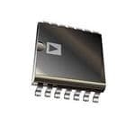
ICGOO电子元器件商城为您提供AD8343ARUZ由Analog设计生产,在icgoo商城现货销售,并且可以通过原厂、代理商等渠道进行代购。 AD8343ARUZ价格参考¥33.50-¥40.20。AnalogAD8343ARUZ封装/规格:RF 混频器, RF Mixer IC Cellular, WLAN Up/Down Converter 0Hz ~ 2.5GHz 14-TSSOP。您可以下载AD8343ARUZ参考资料、Datasheet数据手册功能说明书,资料中有AD8343ARUZ 详细功能的应用电路图电压和使用方法及教程。
| 参数 | 数值 |
| 产品目录 | |
| 描述 | IC MXR 0HZ-2.5GHZ UP/DWN 14TSSOP射频混合器 DC-to-2.5GHz Hi IP3 |
| 产品分类 | |
| 品牌 | Analog Devices Inc |
| 产品手册 | |
| 产品图片 |
|
| rohs | 符合RoHS无铅 / 符合限制有害物质指令(RoHS)规范要求 |
| 产品系列 | RF集成电路,射频混合器,Analog Devices AD8343ARUZAD8343 |
| 数据手册 | |
| 产品型号 | AD8343ARUZ |
| RF类型 | 手机,WLAN |
| 产品目录页面 | |
| 产品种类 | 射频混合器 |
| 供应商器件封装 | 14-TSSOP |
| 包装 | 管件 |
| 商标 | Analog Devices |
| 噪声系数 | 14dB |
| 增益 | 7dB |
| 安装风格 | SMD/SMT |
| 封装 | Tube |
| 封装/外壳 | 14-TSSOP(0.173",4.40mm 宽) |
| 封装/箱体 | TSSOP-14 |
| 工作电源电压 | 5 V |
| 工厂包装数量 | 96 |
| 最大功率耗散 | 320 mW |
| 最大工作温度 | + 85 C |
| 最小工作温度 | - 40 C |
| 标准包装 | 96 |
| 混频器数 | 1 |
| 电压-电源 | 4.5 V ~ 5.5 V |
| 电流-电源 | 60mA |
| 电源电流 | 50 mA |
| 类型 | Mixers |
| 系列 | AD8343 |
| 视频文件 | http://www.digikey.cn/classic/video.aspx?PlayerID=1364138032001&width=640&height=505&videoID=2245193150001 |
| 转换损失——最大 | 7 dB |
| 辅助属性 | 升/降频器 |
| 频率 | 0Hz ~ 2.5GHz |
| 频率范围 | 50 MHz to 2.5 GHz |


- 商务部:美国ITC正式对集成电路等产品启动337调查
- 曝三星4nm工艺存在良率问题 高通将骁龙8 Gen1或转产台积电
- 太阳诱电将投资9.5亿元在常州建新厂生产MLCC 预计2023年完工
- 英特尔发布欧洲新工厂建设计划 深化IDM 2.0 战略
- 台积电先进制程称霸业界 有大客户加持明年业绩稳了
- 达到5530亿美元!SIA预计今年全球半导体销售额将创下新高
- 英特尔拟将自动驾驶子公司Mobileye上市 估值或超500亿美元
- 三星加码芯片和SET,合并消费电子和移动部门,撤换高东真等 CEO
- 三星电子宣布重大人事变动 还合并消费电子和移动部门
- 海关总署:前11个月进口集成电路产品价值2.52万亿元 增长14.8%


PDF Datasheet 数据手册内容提取
DC-to-2.5 GHz High IP3 Active Mixer AD8343 FEATURES FUNCTIONAL BLOCK DIAGRAM High-performance active mixer AD8343 Broadband operation to 2.5 GHz COMM 1 14 COMM Conversion gain: 7 dB INPP 2 13 OUTP Input IP3: 16.5 dBm INPM 3 12 OUTM LO drive: –10 dBm DCPL 4 11 COMM Noise figure: 14 dB VPOS 5 10 LOIP Input P : 2.8 dBm 1dB BIAS Differential LO, IF and RF Ports PWDN 6 9 LOIM 5Si0n Ωgl LeO-s uinpppulyt iomppeeradtaionnce: 5 V @ 50 mA typical COMM 7 8 COMM 01034-001 Power-down mode @ 20 μA typical Figure 1. APPLICATIONS Cellular base stations Wireless LAN Satellite converters SONET/SDH radio Radio links RF instrumentation GENERAL DESCRIPTION The LO driver circuitry typically consumes 15 mA of current. Two external resistors are used to set the mixer core current for The AD8343 is a high-performance broadband active mixer. required performance, resulting in a total current of 20 mA to With wide bandwidth on all ports and very low intermodula- 60 mA. This corresponds to power consumption of 100 mW to tion distortion, the AD8343 is well suited for demanding 300 mW with a single 5 V supply. transmit applications or receive channel applications. The AD8343 is fabricated on Analog Devices, Inc.’s high- The AD8343 provides a typical conversion gain of 7 dB. The performance 25 GHz silicon bipolar IC process. The AD8343 is integrated LO driver supports a 50 Ω differential input imped- available in a 14-lead TSSOP package. It operates over a −40°C ance with low LO drive level, helping to minimize external to +85°C temperature range. A device-populated evaluation component count. board is available. The open-emitter differential inputs can be interfaced directly to a differential filter or driven through a balun (transformer) to provide a balanced drive from a single-ended source. The open-collector differential outputs can be used to drive a differential IF signal interface or convert to a single-ended signal through the use of a matching network or transformer. When centered on the VPOS supply voltage, the outputs swing ±1 V. Rev. B Information furnished by Analog Devices is believed to be accurate and reliable. However, no responsibility is assumed by Analog Devices for its use, nor for any infringements of patents or other One Technology Way, P.O. Box 9106, Norwood, MA 02062-9106, U.S.A. rights of third parties that may result from its use. Specifications subject to change without notice. No license is granted by implication or otherwise under any patent or patent rights of Analog Devices. Tel: 781.329.4700 www.analog.com Trademarks and registered trademarks are the property of their respective owners. Fax: 781.461.3113 ©2006 Analog Devices, Inc. All rights reserved.
AD8343 TABLE OF CONTENTS Features..............................................................................................1 Power-Down Interface (PWDN).............................................16 Applications.......................................................................................1 AC Interfaces...................................................................................17 Functional Block Diagram..............................................................1 Input Interface (INPP and INPM)...............................................18 General Description.........................................................................1 Single-Ended-to-Differential Conversion...............................18 Revision History...............................................................................2 Input Matching Considerations...............................................18 Specifications.....................................................................................3 Input Biasing Considerations...................................................19 Basic Operating Instructions......................................................3 Output Interface (OUTP, OUTM)...............................................20 Typical AC Performance..............................................................4 Output Matching Considerations............................................20 Typical Isolation Performance....................................................4 Output Biasing Considerations................................................20 Absolute Maximum Ratings............................................................5 Input and Output Stability Considerations.................................21 ESD Caution..................................................................................5 Local Oscillator Input Interface (LOIP, LOIM).....................22 Pin Configuration and Function Descriptions.............................6 DC Coupling the LO..................................................................22 Simplified Interface Schematics.................................................7 A Step-by-Step Approach to Impedance Matching...............23 Typical Performance Characteristics.............................................8 Applications.....................................................................................26 Receiver Characteristics..............................................................8 Downconverting Mixer.............................................................26 Transmit Characteristics............................................................13 Upconverting Mixer...................................................................26 Circuit Description.........................................................................15 Evaluation Board............................................................................27 DC Interfaces..................................................................................16 Outline Dimensions.......................................................................32 Biasing and Decoupling (VPOS, DCPL).................................16 Ordering Guide..........................................................................32 REVISION HISTORY 11/06—Rev. A to Rev. B 3/02—Rev. 0 to Rev. A Changes to General Description....................................................1 Edits to Absolute Maximum Ratings..............................................3 Changes to Table 1............................................................................3 Edits to Input Interface (LOIP, LOIM)........................................17 Changes to Table 3............................................................................4 Edits to Table III.............................................................................22 Changes to Power-Down Interface (PWDN) Section...............16 Edits to Table IV.............................................................................23 Changes to Output Matching Considerations Section..............20 Edits to Table V...............................................................................23 Changes to Circuit Description Section......................................15 Edits to Figure 23............................................................................23 Changes to Output Matching Considerations............................20 Edits to Figure 24............................................................................23 Changes to Upconverting Mixer Section....................................26 6/00—Revision 0—Initial Version Changes to Table 6, Table 7, and Table 8.....................................27 Changes to Figure 71 and Figure 72.............................................29 Updated Outline Dimensions.......................................................32 Changes to Ordering Guide..........................................................32 Rev. B | Page 2 of 32
AD8343 SPECIFICATIONS BASIC OPERATING INSTRUCTIONS V = 5.0 V, T = 25°C, unless otherwise noted. S A Table 1. Parameter Conditions/Comments Min Typ Max Unit INPUT INTERFACE (INPP, INPM) Differential Open Emitter DC Bias Voltage Internally generated 1.1 1.2 1.3 V Operating Current Each Input (I ) Current set by R3, R4; see Figure 72 5 17.6 20 mA O Value of Bias Setting Resistor1 1% bias resistors; R3, R4; see Figure 72 68.1 Ω Port Differential Impedance f = 50 MHz; R3 and R4 = 68.1 Ω; see Figure 57 5.6 + j 1.4 Ω OUTPUT INTERFACE (OUTP, OUTM) Differential Open Collector DC Bias Voltage Externally applied 4.5 5 5.5 V Voltage Swing Collector bias (V) = VPOS 1.65 V ± 1 V + 2 V S S S Operating Current Each Output Same as input current I mA O Port Differential Impedance f = 50 MHz; see Figure 60 900 − j 77 Ω LO INTERFACE (LOIP, LOIM) Differential Common Base Stage DC Bias Voltage2 Internally generated; (port is typically ac-coupled) 300 360 450 mV LO Input Power 50 Ω impedance; see Figure 65 −12 −10 −3 dBm Port Differential Reflection Coefficient See Figure 64 −10 dB POWER-DOWN INTERFACE (PWDN) PWDN Threshold Assured on V − 1.5 V S Assured off V − 0.5 V S PWDN Response Time3 Time from device on to off; see Figure 52 2.2 μs Time from device off to on; see Figure 53 500 ns PWDN Input Bias Current PWDN = 0 V (device on) −160 −250 μA PWDN = 5 V (device off) 0 μA POWER SUPPLY Supply Voltage Range 4.5 5.0 5.5 V Total Quiescent Current R3 and R4 = 68.1 Ω; see Figure 72 50 60 mA Over temperature 75 mA Powered-Down Current V = 5.5 V 20 95 μA S V = 4.5 V 6 15 μA S Over temperature; V = 5.5 V 50 150 μA S 1 The balance in the bias current in the two legs of the mixer input is important to applications where a low feedthrough of the local oscillator (LO) is critical. 2 This voltage is proportional to absolute temperature (PTAT). See the DC Coupling the LO section for more information regarding this interface. 3 Response time until device meets all specified conditions. Rev. B | Page 3 of 32
AD8343 TYPICAL AC PERFORMANCE V = 5.0 V, T = 25°C; see Figure 72, Table 6 through Table 8. S A Table 2. Conversion SSB Noise Input 1 dB Compression Input Frequency (MHz) Output Frequency (MHz) Gain (dB) Figure (dB) Input IP3 (dBm) Point (dBm) RECEIVER CHARACTERISTICS 400 70 5.6 10.5 20.5 3.3 900 170 3.6 11.4 19.4 3.6 1900 170 7.1 14.1 16.5 2.8 2400 170 6.8 15.3 14.5 2.1 2400 425 5.4 16.2 16.5 2.2 TRANSMITTER CHARACTERISTICS 150 900 7.5 17.9 18.1 1.9 150 1900 0.25 16.0 13.4 0.8 TYPICAL ISOLATION PERFORMANCE V = 5.0 V, T = 25°C; see Figure 72, Table 6 through Table 8. S A Table 3. LO to Output 2xLO to Output 3xLO to Output Input to Output Input Frequency (MHz) Output Frequency (MHz) Leakage (dBm) Leakage (dBm) Leakage (dBm) Leakage (dBm) RECEIVER CHARACTERISTICS 400 70 −40.1 −51.0 −44.0 −62.4 900 170 −44.4 −35.5 <−75.0 −56.9 1900 170 −65.6 −38.3 −73.3 −65.7 2400 170 −66.7 −44.4 <−73.7 −73.7 2400 425 −51.1 −49.4 <−75.0 −92.3 TRANSMITTER CHARACTERISTICS 150 900 −30 −32 −62 −50 150 1900 −25 −17 −65 −40 Rev. B | Page 4 of 32
AD8343 ABSOLUTE MAXIMUM RATINGS Table 4. Stresses above those listed under Absolute Maximum Ratings Parameter Rating may cause permanent damage to the device. This is a stress VPOS Quiescent Voltage 5.5 V rating only; functional operation of the device at these or any OUTP, OUTM Quiescent Voltage 5.5 V other conditions above those indicated in the operational INPP, INPM Voltage Differential 500 mV section of this specification is not implied. Exposure to absolute (Either Polarity) maximum rating conditions for extended periods may affect LOIP, LOIM Current 1 mA (Injection or Extraction) device reliability. LOIP, LOIM Voltage Differential 500 mV ESD CAUTION (Either Polarity) Internal Power Dissipation (TSSOP)1 320 mW θ (TSSOP) 125°C/W JA Maximum Junction Temperature 125°C Operating Temperature Range −40°C to + 85°C Storage Temperature Range −65°C to +150°C Lead Temperature (Soldering 60 sec) 300°C 1 A portion of the device power is dissipated by external bias resistors, R3 and R4. Rev. B | Page 5 of 32
AD8343 PIN CONFIGURATION AND FUNCTION DESCRIPTIONS COMM 1 14 COMM AD8343 INPP 2 13 OUTP TOP VIEW INPM 3 (Not to Scale)12 OUTM DCPL 4 11 COMM VPOS 5 10 LOIP PWDN 6 9 LOIM COMM 7 8 COMM 01034-002 Figure 2. Pin Configuration Table 5. Pin Function Descriptions Pin No. Mnemonic Description 1, 7, 8, 11, 14 COMM Connect to low impedance circuit ground. 2 INPP Differential Input Pin. This pin needs to be dc-biased and typically ac-coupled; see Figure 3. 3 INPM Differential Input Pin. This pin needs to be dc-biased and typically ac-coupled; see Figure 3. 4 DCPL Bias rail decoupling capacitor connection for LO driver; see Figure 6. 5 VPOS Positive Supply Voltage (V), 4.5 V to 5.5 V. Ensure adequate supply bypassing for proper device operation as S shown in the Applications section. 6 PWDN Power-Down Interface. Connect pin to ground for normal operating mode. Connect pin to supply for power- down mode; see Figure 5. 9 LOIM Differential Local Oscillator (LO) Input Pin. Typically ac-coupled; see Figure 4. 10 LOIP Differential Local Oscillator (LO) Input Pin. Typically ac-coupled; see Figure 4. 12 OUTM Open-Collector Differential Output Pin. This pin needs to be dc-biased and (usually) ac-coupled; see Figure 3. 13 OUTP Open-Collector Differential Output Pin. This pin needs to be dc-biased and (usually) ac-coupled; see Figure 3. Rev. B | Page 6 of 32
AD8343 SIMPLIFIED INTERFACE SCHEMATICS VPOS OUTP OUTM 5VDC 5VDC 5VDC LOIP VPOS LOIM 5VDC VPOS INPP 1.2VDC 5VDC 25kΩ PWDN INPM 1.2VDC 01034-003 CBEIALSL 01034-005 Figure 3. Input and Output Ports Figure 5. Power-Down Pin 2VDC DCPL BIAS VPOS VPOS CELL R1 5VDC 10Ω VBIAS 360mVDC 360mVDC LOIP LOIP LO TO LOIM 360mVDC 400Ω 400Ω 01034-004 LOIM 360mVDC BUFFER MCOIXREER 01034-006 Figure 4. LO Port Figure 6. Bias Decoupling Pin Rev. B | Page 7 of 32
AD8343 TYPICAL PERFORMANCE CHARACTERISTICS RECEIVER CHARACTERISTICS f = 400 MHz, f = 70 MHz, f = 330 MHz, see Figure 72, Table 6, and Table 8. IN OUT LO 60 10 MEAN: 5.57dB 50 9 B) d E 40 N ( 8 ENTAG 30 ON GAI 7 PERC 20 NVERSI 6 O C 10 5 0 01034-007 4 01034-010 5.37 5.42 5.47 5.52 5.57 5.62 5.67 5.72 –40 –20 0 20 40 60 80 CONVERSION GAIN (dB) TEMPERATURE (°C) Figure 7. Gain Histogram; fIN = 400 MHz, fOUT = 70 MHz Figure 10. Gain Performance Over Temperature; fIN = 400 MHz, fOUT = 70 MHz 25 24 MEAN: 20.5dBm 23 20 22 GE 15 Bm) 21 CENTA T IP3 (d 1290 R U E 10 P P N I 18 17 5 0 01034-008 1156 01034-011 19.9 20.0 20.1 20.2 20.3 20.4 20.5 20.6 20.7 20.8 20.9 21.0 –40 –20 0 20 40 60 80 INPUT IP3 (dBm) TEMPERATURE (°C) Figure 8. Input IP3 Histogram; fIN = 400 MHz, fOUT = 70 MHz Figure 11. Input IP3 Performance Over Temperature; fIN = 400 MHz, fOUT = 70 MHz 60 5.0 55 MEAN: 3.31dB m) 50 dB 4.5 45 NT ( OI 40 P 4.0 CENTAGE 3305 RESSION 3.5 ER 25 MP P O 20 C 3.0 B 15 1d T 10 PU 2.5 05 01034-009 IN 2.0 01034-012 3.24 3.26 3.28 3.30 3.32 3.34 3.36 3.38 –40 –20 0 20 40 60 80 INPUT 1dB COMPRESSION POINT (dBm) TEMPERATURE (°C) Figure 9. Input 1 dB Compression Point Histogram; fIN = 400 MHz, Figure 12. Input 1 dB Compression Point Performance Over Temperature; fOUT = 70 MHz fIN = 400 MHz, fOUT = 70 MHz Rev. B | Page 8 of 32
AD8343 f = 900 MHz, f = 170 MHz, f = 730 MHz, see Figure 72, Table 6, and Table 8. IN OUT LO 35 6 30 5 MEAN: 3.63dB 25 B) E N (d 4 AG 20 GAI ENT ON 3 PERC 15 VERSI N 2 10 O C 1 5 0 01034-013 0 01034-016 3.40 3.45 3.50 3.55 3.60 3.65 3.70 3.75 3.80 3.85 –40 –20 0 20 40 60 80 CONVERSION GAIN (dB) TEMPERATURE (°C) Figure 13. Gain Histogram; fIN = 900 MHz, fOUT = 170 MHz Figure 16. Gain Performance Over Temperature; fIN = 900 MHz , fOUT = 170 MHz 30 23 28 26 22 24 MEAN: 19.4dBm 22 21 E 20 m) 20 G 18 B A d PERCENT 111246 NPUT IP3 ( 1189 10 I 8 17 6 240 01034-014 1156 01034-017 18.2 18.4 18.6 18.8 19.0 19.2 19.4 19.6 19.8 20.0 20.2 20.4 –40 –20 0 20 40 60 80 INPUT IP3 (dBm) TEMPERATURE (°C) Figure 14. Input IP3 Histogram; fIN = 900 MHz, fOUT = 170 MHz Figure 17. Input IP3 Performance Over Temperature; fIN = 900 MHz, fOUT = 170 MHz 30 5.0 28 MEAN: 3.62dBm m) 26 B 4.5 d 24 T ( 22 OIN 20 P 4.0 E N G 18 O PERCENTA 11110246 B COMPRESSI 33..05 8 1d 6 UT 2.5 P 024 01034-015 IN 2.0 01034-018 3.52 3.54 3.56 3.58 3.60 3.62 3.64 3.66 3.68 3.70 3.72 –40 –20 0 20 40 60 80 INPUT 1dB COMPRESSION POINT (dBm) TEMPERATURE (°C) Figure 15. Input 1 dB Compression Point Histogram; fIN = 900 MHz, Figure 18. Input 1dB Compression Point Performance Over Temperature; fOUT = 170 MHz fIN = 900 MHz, fOUT = 170 MHz Rev. B | Page 9 of 32
AD8343 f = 1900 MHz, f = 170 MHz, f = 1730 MHz, see Figure 72, Table 6, and Table 8. IN OUT LO 28 10 26 MEAN: 7.09dB 24 9 22 20 B) GE 18 AIN (d 8 A 16 G ENT 14 ON 7 RC 12 RSI E E P 10 NV 6 8 CO 6 5 4 02 01034-019 4 01034-022 6.75 6.80 6.85 6.90 6.95 7.00 7.05 7.10 7.15 7.20 7.25 7.30 –40 –20 0 20 40 60 80 CONVERSION GAIN (dB) TEMPERATURE (°C) Figure 19. Gain Histogram; fIN = 1900 MHz, fOUT = 170 MHz Figure 22. Gain Performance Over Temperature; fIN = 1900 MHz, fOUT = 170 MHz 45 18 40 MEAN: 16.54dBm 17 35 16 E 30 m) 15 G B CENTA 2250 T IP3 (d 14 R U PE NP 13 15 I 12 10 50 01034-020 1101 01034-023 14.0 14.5 15.0 15.5 16.0 16.5 17.0 17.5 18.0 18.5 –40 –20 0 20 40 60 80 INPUT IP3 (dBm) TEMPERATURE (°C) Figure 20. Input IP3 Histogram; fIN = 1900 MHz, fOUT = 170 MHz Figure 23. Input IP3 Performance Over Temperature; fIN = 1900 MHz, fOUT = 170 MHz 50 5.0 45 MEAN: 2.8dBm m) B 4.5 d 40 T ( N 35 OI P 4.0 E N G 30 O PERCENTA 2250 COMPRESSI 33..05 15 B d 1 10 UT 2.5 P 50 01034-021 IN 2.0 01034-024 2.60 2.65 2.70 2.75 2.80 2.85 2.90 2.95 3.00 3.05 –40 –20 0 20 40 60 80 INPUT 1dB COMPRESSION POINT (dBm) TEMPERATURE (°C) Figure 21. Input 1 dB Compression Point Histogram; fIN = 1900 MHz, Figure 24. Input 1 dB Compression Point Performance Over Temperature; fOUT = 170 MHz fIN = 1900 MHz, fOUT = 170 MHz Rev. B | Page 10 of 32
AD8343 f = 2400 MHz, f = 170 MHz, f = 2230 MHz, see Figure 72, Table 6, and Table 8. IN OUT LO 40 10 35 MEAN: 6.79dB 9 30 B) E 25 N (d 8 G AI A G ENT 20 ON 7 PERC 15 VERSI N 6 O 10 C 5 05 01034-025 4 01034-028 5.8 6.0 6.2 6.4 6.6 6.8 7.0 7.2 7.4 7.6 –40 –20 0 20 40 60 80 CONVERSION GAIN (dB) TEMPERATURE (°C) Figure 25. Gain Histogram; fIN = 2400 MHz, fOUT = 170 MHz Figure 28. Gain Performance Over Temperature; fIN = 2400 MHz, fOUT = 170 MHz 35 18 30 MEAN: 14.46dBm 17 16 25 E m) 15 G B A 20 d RCENT 15 UT IP3 ( 14 PE NP 13 I 10 12 50 01034-026 1101 01034-029 13.013.213.413.613.814.014.214.414.614.815.015.215.415.6 –40 –20 0 20 40 60 80 INPUT IP3 (dBm) TEMPERATURE (°C) Figure 26. Input IP3 Histogram; fIN = 2400 MHz, fOUT = 170 MHz Figure 29. Input IP3 Performance Over Temperature; fIN = 2400 MHz, fOUT = 170 MHz 45 3.0 40 INPUT: 2.11dBm m) B 2.5 d 35 T ( N 30 POI 2.0 E N G O PERCENTA 2250 OMPRESSI 1.5 15 C 1.0 B d 10 T 1 U 0.5 P 05 01034-027 IN 0 01034-030 1.90 1.95 2.00 2.05 2.10 2.15 2.20 2.25 2.30 2.35 2.40 –40 –20 0 20 40 60 80 INPUT 1dB COMPRESSION POINT (dBm) TEMPERATURE (°C) Figure 27. Input 1 dB Compression Point Histogram; fIN = 2400 MHz, Figure 30. Input 1 dB Compression Point Performance Over Temperature; fOUT = 170 MHz fIN = 2400 MHz, fOUT = 170 MHz Rev. B | Page 11 of 32
AD8343 f = 2400 MHz, f = 425 MHz, f = 1975 MHz, see Figure 72, Table 6, and Table 8. IN OUT LO 24 10 22 MEAN: 5.40dB 20 9 18 B) E 16 N (d 8 ENTAG 1124 ON GAI 7 PERC 108 NVERSI 6 O 6 C 4 5 02 01034-031 4 01034-034 4.2 4.4 4.6 4.8 5.0 5.2 5.4 5.6 5.8 6.0 6.2 6.4 6.6 –40 –20 0 20 40 60 80 CONVERSION GAIN (dB) TEMPERATURE (°C) Figure 31. Gain Histogram; fIN = 2400 MHz, fOUT = 425 MHz Figure 34. Gain Performance Over Temperature; fIN = 2400 MHz, fOUT = 425 MHz 22 18 20 MEAN: 16.50dBm 17 18 16 16 GE 14 m) 15 A B T 12 d PERCEN 108 NPUT IP3 ( 1134 I 6 12 4 028 0 2 4 6 8 0 2 4 6 8 0 2 4 6 8 001034-032 1101 01034-035 4. 5. 5. 5. 5. 5. 6. 6. 6. 6. 6. 7. 7. 7. 7. 7. 8. –40 –20 0 20 40 60 80 1 1 1 1 1 1 1 1 1 1 1 1 1 1 1 1 1 INPUT IP3 (dBm) TEMPERATURE (°C) Figure 32. Input IP3 Histogram; fIN = 2400 MHz, fOUT = 425 MHz Figure 35. Input IP3 Performance Over Temperature; fIN = 2400 MHz, fOUT = 425 MHz 65 3.0 60 MEAN: 2.22dBm 55 m) B 2.5 50 T (d GE 4405 N POIN 2.0 A O PERCENT 233505 MPRESSI 1.5 O 20 C 1.0 B 15 1d T 10 U 0.5 052.00 2.05 2.10 2.15 2.20 2.25 2.30 2.35 2.40 2.45 2.501034-0330 INP 0 01034-036 –40 –20 0 20 40 60 80 INPUT 1dB COMPRESSION POINT (dBm) TEMPERATURE (°C) Figure 33. Input 1 dB Compression Point Histogram; fIN = 2400 MHz, Figure 36. Input 1 dB Compression Point Performance Over Temperature; fOUT = 425 MHz fIN = 2400 MHz, fOUT = 425 MHz Rev. B | Page 12 of 32
AD8343 TRANSMIT CHARACTERISTICS f = 150 MHz, f = 900 MHz, f = 750 MHz, see Figure 72, Table 6, and Table 7. IN OUT LO 35 10 30 MEAN: 7.49dBm 9 25 B) E N (d 8 G AI A 20 G ENT ON 7 RC 15 RSI E E P V N 6 10 CO 5 5 0 01034-037 4 01034-040 7.20 7.25 7.30 7.35 7.40 7.45 7.50 7.55 7.60 7.65 7.70 –40 –20 0 20 40 60 80 CONVERSION GAIN (dB) TEMPERATURE (°C) Figure 37. Gain Histogram; fIN = 150 MHz, fOUT = 900 MHz Figure 40. Gain Performance Over Temperature; fIN = 150 MHz, fOUT = 900 MHz 24 22 MEAN: 18.1dBm 20 20 19 18 16 18 E RCENTAG 111024 P3 (dBm) 1176 PE T I 8 U NP 15 6 I 4 14 027.80 7.85 7.90 7.95 8.00 8.05 8.10 8.15 8.20 8.25 8.30 8.35 8.40 8.4501034-038 1123 01034-041 1 1 1 1 1 1 1 1 1 1 1 1 1 1 –40 –20 0 20 40 60 80 INPUT IP3 (dBm) TEMPERATURE (°C) Figure 38. Input IP3 Histogram; fIN = 150 MHz, fOUT = 900 MHz Figure 41. Input IP3 Performance Over Temperature; fIN = 150 MHz, fOUT = 900 MHz 24 3.0 22 MEAN: 1.9dBm 20 2.5 m) 18 B d 16 N ( 2.0 AGE 14 ESIO T R EN 12 MP 1.5 C O R 10 C PE B 8 1d 1.0 T 6 U P N 4 I 0.5 02 01034-039 0 01034-042 1.551.601.651.701.751.801.851.901.952.002.052.102.152.20 –40 –20 0 20 40 60 80 INPUT 1dB COMPRESSION POINT (dBm) TEMPERATURE (°C) Figure 39. Input 1 dB Compression Point Histogram; Figure 42. Input 1dB Compression Point Performance Over Temperature; fIN = 150 MHz, fOUT = 900 MHz fIN = 150 MHz, fOUT = 900 MHz Rev. B | Page 13 of 32
AD8343 f = 150 MHz, f = 1900 MHz, f = 1750 MHz, see Figure 72, Table 6, and Table 7. IN OUT LO 40 5 35 MEAN: 0.25dB 4 30 B) 3 d AGE 25 GAIN ( 2 ENT 20 ON PERC 15 VERSI 1 N 10 CO 0 –1 50 01034-043 –2 01034-046 –1.0 –0.8 –0.6 –0.4 –0.2 0 0.2 0.4 0.6 0.8 1.0 1.2 1.4 –40 –20 0 20 40 60 80 CONVERSION GAIN (dB) TEMPERATURE (°C) Figure 43. Gain Histogram; fIN = 150 MHz, fOUT = 1900 MHz Figure 46. Gain Performance Over Temperature; fIN = 150 MHz, fOUT = 1900 MHz 50 18 45 MEAN: 13.4dBm 17 40 16 35 ENTAGE 2350 P3 (dBm) 1154 RC T I 13 E 20 U P P N 15 I 12 10 11 5010.511.011.512.012.513.013.514.014.515.015.516.016.517.001034-044 109–40 –20 0 20 40 60 80 01034-047 INPUT IP3 (dBm) TEMPERATURE (°C) Figure 44. Input IP3 Histogram; fIN = 150 MHz, fOUT = 1900 MHz Figure 47. Input IP3 Performance Over Temperature; fIN = 150 MHz, fOUT = 1900 MHz 45 2.0 40 MEAN: 0.79dBm m) B 1.5 d 35 T ( N OI 30 P 1.0 TAGE 25 SION EN ES 0.5 RC 20 PR E M P O 15 C 0 B d 10 T 1 PU –0.5 50 01034-045 IN –1.0 01034-048 –1.0 –0.5 0 0.5 1.0 1.5 2.0 2.5 3.0 3.5 –40 –20 0 20 40 60 80 INPUT 1dB COMPRESSION POINT (dBm) TEMPERATURE (°C) Figure 45. Input 1 dB Compression Point Histogram; fIN = 150 MHz, Figure 48. Input 1 dB Compression Point Performance Over Temperature; fOUT = 1900 MHz fIN = 150 MHz, fOUT = 1900 MHz Rev. B | Page 14 of 32
AD8343 CIRCUIT DESCRIPTION Unfortunately, practical implementations of analog multipliers The AD8343 is a mixer intended for high-intercept applications. generally make poor mixers because of imperfect linearity and The signal paths are entirely differential and dc-coupled to the added noise that invariably accompanies attempts to improve permit high-performance operation over a broad range of linearity. The best mixers to date are those that use the LO frequencies; the block diagram (see Figure 1) shows the basic signal to periodically reverse the polarity of the input signal. functional blocks. The bias cell provides a PTAT (proportional to absolute temperature) bias to the LO driver and core. The LO In this class of mixers, frequency conversion occurs as a driver consists of a three-stage limiting differential amplifier result of multiplication of the signal by a square wave at the that provides a very fast (almost square-wave) drive to the bases LO frequency. Because a square wave contains odd harmonics of the core transistors. in addition to the fundamental, the signal is effectively multi- plied by each frequency component of the LO. The output of The AD8343 core utilizes a standard architecture where the the mixer therefore contains signals at F ± F , 3×F ± F , signal inputs are directly applied to the emitters of the transis- LO sig LO sig 5× F ± F , 7×F ± F , etc. The amplitude of the components tors in the cell (see Figure 49 and Figure 55). The bases are LO sig LO sig arising from signal multiplication by LO harmonics falls off driven by the hard-limited LO signal that directs the transistors with increasing harmonic order because the amplitude of a to steer the input currents into periodically alternating pairs of square wave’s harmonics falls off. output terminals, thus providing the periodic polarity reversal that effectively multiplies the signal by a square wave of the LO An example of this process is illustrated in Figure 50. The first frequency. pane of this figure shows an 800 MHz sinusoid intended to VPOS COMM represent an input signal. The second pane contains a square 5 1 7 8 11 14 wave representing an LO signal at 600 MHz which has been AD8343 hard-limited by the internal LO driver. The third pane shows DCPL 4 MIXER 13 OUTP the time domain representation of the output waveform and the BIAS CORE PWDN 6 12 OUTM fourth pane shows the frequency domain representation. The Q1 Q2 Q3 Q4 two strongest lines in the spectrum are the sum and difference LOIP 10 frequencies arising from multiplication of the signal by the LOs LOIM 9 fundamental frequency. The weaker spectral lines are the result DRLIVOER 2 3 01034-049 oLfO t hseq umaurelt wipalivcea.t ion of the signal by various harmonics of the INPP INPM Figure 49. Topology To illustrate this functionality, when LOIP is positive, Q1 SIGNAL and Q4 are turned on, and Q2 and Q3 are turned off. In this condition, Q1 connects I to OUTM and Q4 connects I INPP INPM to OUTP. When LOIP is negative, the roles of the transistors TIME LOCAL DOMAIN OSCILLATOR reverse, steering I to OUTP and I to OUTM. Isolation INPP INPM and gain are possible because, at any instant, the signal passes through a common-base transistor amplifier pair. SIG × LO Multiplication is the essence of frequency mixing; an ideal multiplier would make an excellent mixer. The theory is expressed in the following trigonometric identity: FREQUENCY SIG × LO DOMAIN sin(ω t) × sin(ω t) = ½[cos(ω t − ω t) − cos(ω t + ω t)] sig LO sig LO sig LO O G O G G G G Tfrheqisu setnacteies st hisa at tphaei rp orof dsiuncet wofa vtweso a sti nfree-qwuaevnec sieigs neaqlus aolf t doi tfhfeer ent SIG – L LO – SI SIG + L LO – SI LO + SI LO – SI LO + SI sum and difference of the two frequencies being multiplied. 3 × FREQU5 × ENCY3 × 7 × 5 × 01034-050 Figure 50. Signal Switching Characteristics of the AD8343 Rev. B | Page 15 of 32
AD8343 DC INTERFACES BIASING AND DECOUPLING (VPOS, DCPL) VPOS is the power supply connection for the internal bias circuit and the LO driver. Bypass this pin closely to GND with a capacitor in the range of 0.01 μF to 0.1 μF. The DCPL pin provides access to an internal bias node for noise bypassing 1 purposes. Bypass this node to COMM with 0.1 μF. POWER-DOWN INTERFACE (PWDN) The AD8343 is active when the PWDN pin is held low; other- 2 wise the device enters a low-power state as shown in Figure 51. 4405 PSOWWEPETR -FDROOWMN CH1 200nVΩ CH2 1.00VΩ M500ns CH2 4.48V 01034-052 BOTH 3V TO 5V 35 AND 5V TO 3V Figure 52. PWDN Response Time Device On to Off A) m 30 T ( N E 25 R R U C 20 E C VI 15 E D 1 10 05 01034-051 3.0 3.5 4.0 4.5 5.0 2 POWER-DOWN VOLTAGE (V) To assure full Fpioguwree r5-1d. oDwevnic,e t Chuer rPeWnt vDs.N PW vDoNlt aVgoelt amgue st be within 01034-053 CH1 200nVΩ CH2 1.00VΩ M100ns CH2 4.48V 0.5 V of the supply voltage at VPOS. Normal operation requires Figure 53. PWDN Response Time Device Off to On that the PWDN pin be taken at least 1.5 V below the supply voltage. The PWDN pin sources about 160 μA when pulled to TRIGGER TEKTRONIX TDS694C GND (see the Pin Configuration and Function Descriptions OSCILLOSCOPE IF OUTPUT 170MHz HP8648C section). It is not advised to leave the pin floating when the SIGNAL GENERATOR AD8343 device is disabled; a resistive pull-up to VPOS is the minimum RF INPUT 1 COMM COMM 14 suggestion. 1740MHz The AD8343 requires about 2.2 μs to turn off when PWDN is MATCHING 2 INPP OUTP13 MATCHING NETWORK AND NETWORK AND asserted; turn-on time is about 500 ns. Figure 52 and Figure 53 TRANSFORMER 3 INPM OUTM12 TRANSFORMER show typical characteristics (they vary with bypass component 0.1µF 4 DCPL COMM 11 values). Figure 54 shows the test configuration used to acquire 1nH these waveforms. VPOS 5 VPOS LOIP10 0.1µF TRANSFORMER 6 PWDN LOIM 9 HP8130 LO INPUT PULSE 7 COMM COMM 8 1570MHz GENERATOR GEHSNPIEG8R6N4AA8TLCOR 01034-054 Figure 54. PWDN Response Time Test Schematic Rev. B | Page 16 of 32
AD8343 AC INTERFACES SINGLE-ENDED Because of the AD8343’s wideband design, there are several OUTPUT SIGNAL points to consider in its ac implementation; the basic ac signal connection diagram shown in Figure 55 summarizes these DIFFERENTIAL-TO-SINGLE-ENDED CONVERSION points. The input signal undergoes a single-ended to differential conversion and is then reactively matched to the impedance OUTPUT MATCHING NETWORK presented by the emitters of the core. The matching network CORE BIAS NETWORK also provides bias currents to these emitters. Similarly, the LO 5 1 7 8 11 14 VPOS AD8343 input undergoes a single-ended-to-differential transformation COMM before it is applied to the 50 Ω differential LO port. The differential 4 DCPL BIAS OUTP13 output signal currents appear at open-collectors and are reac- 6 PWDN CELL OUTM12 tively matched and converted to a single-ended signal. LOIP 10 LOIM 9 CORE LO DRIVER INPP INPM 2 3 INPUT MATCHING SINGLE-ENDED-TO-DIFFERENTIAL NETWORK CONVERSION CORE BIAS NETWORK SINGLE-ENDED SINGLE-ENDED-TO-DIFFERENTIAL LO INPUT SIGNAL CONVERSION SININPGULTE S-EIGNNDAELD 01034-055 Figure 55. Basic AC Signal Connection Diagram Rev. B | Page 17 of 32
AD8343 INPUT INTERFACE (INPP AND INPM) SINGLE-ENDED-TO-DIFFERENTIAL CONVERSION caused by the change in Transistor r due to the change in e current. The standard S parameter files are available through The AD8343 is designed to accept differential input signals for Analog Devices. best performance. While a single-ended input can be applied, the signal capacity is reduced by 6 dB. Furthermore, there is no 134Ω cancellation of even-order distortion arising from the nonlinear 68Ω input impedances, so the effective signal handling capacity is 2500MHz reduced even further in distortion-sensitive situations. That is, 1500MHz the intermodulation intercepts are degraded. 1000MHz 500MHz For these reasons, it is strongly recommended that differ 50MHz eton tcioaml smigneraclsia blley parveasielanbteled b taol uthnes ,A thDe8r3e 4a3r’es vinapriuotu. sI nd iasdcdreittieo ann d FREQUENCY (50MHz TO 2500MHz) 01034-057 printed circuit networks that can produce the required balanced Figure 57. Input Differential Impedance (INPP, INPM) for Two Values of waveforms and impedance match. These alternate circuits can R3 and R4 be employed to possibly reduce the component cost of the Figure 57 provides a reasonable starting point for the design mixer and/or improve performance. of the network. However, the particular board traces and pads transform the input impedance at frequencies in excess of about Baluns implemented in transmission line form (also known as 500 MHz. For this reason, it is best to make a differential input common-mode chokes) are useful up to frequencies of around impedance measurement at the board location where the matching 1 GHz to 2 GHz, but are often excessively lossy at the higher network is installed, as a starting point for designing an frequencies that the AD8343 can handle. M/A-COM manufac- accurate matching network. tures these baluns and Murata produces a true surface-mount balun. Coilcraft® and Toko are also manufacturers of RF baluns. Differential impedance measurement is made relatively easy INPUT MATCHING CONSIDERATIONS using a technique presented in an article by Lutz Konstroffer in RF Design, Vol. 22, January 1999, Page 24, 28; entitled “Finding The design of the input matching network must be undertaken the Reflection Coefficient of a Differential One-Port Device.” with two goals in mind: matching the source impedance to the This article presents a mathematical formula for converting input impedance of the AD8343 and providing a dc bias current from a two-port single ended measurement to differential path for the bias setting resistors. impedance. A full two-port measurement is performed using a The maximum power transfer into the device occurs when vector network analyzer with Port 1 and Port 2 connected to the there is a conjugate impedance match between the signal source two differential inputs of the device at the desired measurement and the input of the AD8343. This match is achieved with the plane. The two-port measurement results are then processed differential equivalent of the classic L network, as illustrated in with Konstroffer’s formula. This formula is straightforward and Figure 56. The figure gives two examples of the transformation can be implemented through most RF design packages that can from a single-ended L network to its differential counterpart. read and analyze network analyzer data. The Konstroffer The design of L matching networks is adequately covered in formula is: texts on RF amplifier design (for example, Microwave Transistor (2×S11−S21)(1−S22−S12)+(1−S11−S21)(1+S22−2×S12) Amplifiers by Guillermo Gonzalez). Γs= (2−S21)(1−S22−S12)+(1−S11−S21)(1+S22) L1 L1/2 This measurement can also be made using two ports of a C1 C1 L1/2 4-port vector network analyzer. This instrument, and accompanying software, is capable of directly producing C2 2C2 differential measurements. At low frequencies and I = 16 mA, the differential input L2 L2 O SINGLE-ENDED DIFFERE2NCT2IAL 01034-056 ilomwp e(~da5n Ωce i nse seenr iaets pwoirtths pINarPaPsi tainc din IdNuPctMan ocfe sth teh aAt Dto8t3a4l 3a biso u t Figure 56. Single-Ended-to-Differential Transformation 3 nH). Because of this low value of impedance, it is beneficial to choose a transformer-type balun that can also perform all or Figure 57 shows the differential input impedance of the part of the real value impedance transformation. The turns ratio AD8343 at the pins of the device. The two measurements of the transformer removes some of the matching burden from shown in the figure are for two different core currents set by the differential L-network and should help lead to wider Resistor R3 and Resistor R4; the real value impedance shift is Rev. B | Page 18 of 32
AD8343 bandwidth matches. At frequencies above 1 GHz, the real part value calculated as R = 1.2/I . The resistor values should be BIAS BIAS of the input impedance rises markedly and it becomes more well matched in order to maintain full LO to output isolation; attractive to use a 1:1 balun and rely on the L network for the 1% tolerance resistors are recommended. entire impedance transformation. 20 100 In order to obtain the lowest distortion, the inputs of the AD8343 dB) IONUPTUPTU RTF I F= =9 0107M0MHzHz 90 are driven through external ballast resistors. At low frequencies URE ( 16 LO LOW SIDE INJECTION 80 A) (aubpo vteo apbeorhuat p4s0 02 0M0 HMzH, 1z0), Ωab poeurt s5i dΩe ipse br estitdeer. iTs hapep srpoepcrifiaieted; SE FIG 70 ENT (m RF performance values for the AD8343 apply with these ballast D NOI 12 NOISE FIGURE 60 CURR resistors in use. These resistors improve linearity because their N AN 50 PLY linear ac voltage drop partially swamps the nonlinear voltage GAI 8 TOTAL SUPPLY CURRENT 40 SUP swing occurring on the emitters. N 30 L O A In cases where the use of a lossy balun is unavoidable, it can be ERSI 4 20 TOT V worthwhile to perform simultaneous matching on both the ON GAIN 10 C input and output sides of the balun. The idea is to independently characterize the balun as a two-port device and then arrange a 020 40 60 80 R31 A00ND R142 0(Ω) 140 160 180 2000 01034-058 simultaneous conjugate match for it. Unfortunately, there seems Figure 58. Effect of R3 and R4 Value on Gain and Noise Figure to be no good way to determine the benefit this approach offers in any particular case; it remains necessary to characterize the 25 90 INPUT RF = 900MHz balun and then design and simulate appropriate matching n- OUTPUT IF = 170MHz 80 LO LOW SIDE INJECTION eetfwfoorrt kiss wtoo mrthakweh ailne oisp tthime adli sdceocviesiroyn t.h Oatn teh ien addicjuastitomne tnhta ot fs au ch B (dBm) 20 INPUT IP3 70 T (mA) post-balun-only matching network for best gain differs appre- 1d 60 EN ciniapbulty. fAro bmet ttehra tt awcthiicc ihs ptoro tdryu cae ds ibffeesrte rnett uaprnp rlooassc ha tf othr et hbea lbuanlus n, Bm) AND P 15 5400 PLY CURR enFioetthrw emro orpkrue, r ficonhrfa olsoriwmngea rta il oodnsifs fo.e n re pnetr bfoarlumni nogr tdhees iignnpiuntg m a adticshc,r esetee NPUT IP3 (d 105 TOTAL SUPPLY CURRENT 3200 TOTAL SUP I the section entitled A Step-by-Step Approach to Impedance P1dB 10 MINaPtcUhiTn gB. IASING CONSIDERATIONS 020 40 60 80 R31 A00ND R142 0(Ω) 140 160 180 2000 01034-059 Figure 59. Effect of R3 and R4 Value on Input IP3 and Gain Compression The mixer core bias current of the AD8343 is adjustable from less than 5 mA to a safe maximum of 20 mA. It is important to At higher frequencies where the input impedance of the AD8343 note that the reliability of the AD8343 can be compromised for rises, it is beneficial to insert an inductor in series between each core currents set to higher than 20 mA. The AD8343 is tested to bias resistor and the corresponding input pin in order to mini- ensure that a value of 68.1 Ω ±1% ensures safe operation. mize signal shunting (Figure 72). Practical considerations limit the inductive reactance to a few hundred ohms. The best overall Higher operating currents reduce distortion and affect gain, choice of inductor is the value that places the self-resonant noise figure, and input impedance (Figure 58 and Figure 59). frequency at about the upper end of the desired input frequency As the quiescent current is increased by a factor of N, the real range. Note that there is an RF stability concern that argues in part of the input impedance decreases by N. Assuming that a favor of erring on the side of too small an inductor value; see match is maintained, the signal current increases by √N, but the the Input and Output Stability Considerations section. The signal voltage decreases by √N, exercising a smaller portion of Murata LQW1608A series of inductors (0603 SMT package) the nonlinear V–I characteristic of the common base connected offers values up to 56 nH before the self-resonant frequency mixer core transistors and results in lower distortion. falls below 2.4 GHz. At low frequencies where the magnitude of the complex input For optimal LO-to-output isolation, it is important not to impedance is much smaller than the bias resistor values, ade- connect the dc nodes of the emitter bias inductors together quate biasing can be achieved simply by connecting a resistor in an attempt to share a single bias resistor. Doing so causes from each input to GND. The input terminals are internally isolation degradation arising from V mismatches of the biased at 1.2 V dc (nominal), so each resistor has a resistance BE transistors in the core. Rev. B | Page 19 of 32
AD8343 OUTPUT INTERFACE (OUTP, OUTM) The output of the AD8343 comprises a balanced pair of open The output load impedance must also be kept reasonably low collector outputs. These should be biased to about the same at the image frequency to avoid developing appreciable extra voltage as is connected to VPOS. Connecting them to an appre- voltage swing, which can reduce dynamic range. ciably higher voltage is likely to result in conduction of the ESD If maintaining a good output return loss is not required, a 4:1 to protection network on signal peaks, causing high distortion levels. 8:1 (impedance) flux-coupled transformer can be used to present a On the other hand, setting the dc level of the outputs too low is suitable load to the device and to provide collector bias via a also likely to result in poor device linearity due to collector-base center tap as shown in Figure 69. At all but the lowest output capacitance modulation or saturation of the mixer core transistors. frequencies, it becomes desirable to tune out the output capaci- OUTPUT MATCHING CONSIDERATIONS tance of the AD8343 by connecting an inductor between the output pins. On the other hand, when a good output return loss The AD8343 requires a differential load for much the same is desired, the output can be resistively loaded with a shunt reasons that the input needs a differential source to achieve resistance between the output pins in order to set the real value optimal device performance. In addition, a differential load of output impedance. With selection of both the transformer’s provides the best LO to output isolation and the best input to impedance ratio and the shunting resistance as required, the output isolation. desired total load (~500 Ω) is achieved while optimizing both At low output frequencies, it is usually not appropriate to signal transfer and output return loss. arrange a conjugate match between the device output and At higher output frequencies, the output conductance of the the load, even though doing so maximizes the small signal device becomes higher (see Figure 60), with the consequence conversion gain. This is because the output impedance at low that above about 900 MHz, it does become appropriate to frequencies is quite high (a high resistance in parallel with a perform a conjugate match between the load and the AD8343s small capacitance). See Figure 60 for a plot of the differential output. The device’s own output admittance becomes sufficient output impedance measured at the device pins. This data is to remove the threat of clipping from excessive voltage swing. available in standard file format at the Analog Devices website Just as for the input, it is best to perform differential output (http://www.analog.com); search for AD8343, then click on impedance measurements on the board layout to effectively AD8343 S-Parameters. If a matching high impedance load is develop a good matching network. used, sufficient output voltage swing occurs to cause output clipping even at relatively low input levels, constituting a loss OUTPUT BIASING CONSIDERATIONS of dynamic range. The linear range of voltage swing at each When the output single-ended-to-differential conversion takes output pin is about ±1 V from the supply voltage VPOS. A the form of a transformer whose primary winding is center good compromise is to provide a load impedance of about tapped, simply apply VPOS to the tap, preferably through a 200 Ω to 500 Ω between the output pins at the desired output ferrite bead in series with the tap in order to avoid a common frequency (based on 15 mA to 20 mA bias current at each mode instability problem (see the Input and Output Stability input). At output frequencies below 500 MHz, more output Considerations section). See Figure 69 for an example of this power can be obtained before the onset of gross clipping by network. The collector dc bias voltage must be nominally equal using a lower load impedance; however, both gain and low to the supply voltage applied to Pin 5 (VPOS). order distortion performance can be degraded. If a 1:1 transmission line balun is used for the output, it is FREQUENCY (50MHz TO 2500MHz) necessary to bring in collector bias through separate inductors. These inductors are chosen to obtain a high impedance over the RF output frequency range of interest. See Figure 70 for an 50MHz example of this network. 2000MHz 1500MHz 500MHz 1000MHz 01034-060 Figure 60. Output Differential Impedance (OUTP, OUTM) Rev. B | Page 20 of 32
AD8343 INPUT AND OUTPUT STABILITY CONSIDERATIONS The differential configuration of the input and output ports of the AD8343 raises the need to consider both differential and common-mode RF stability of the device. Throughout the following stability discussion, common mode is used to refer to a signal that is referenced to ground. The equivalent common- 150MHz mode impedance is the value of impedance seen from the node 50MHz under discussion to ground. The book, Microwave Transistor Amplifiers by Guillermo Gonzalez, also has an excellent section covering stability of amplifiers. The AD8343 is unconditionally stable for any differential impedance, so device stability need not be considered with rpeostpeenctita tloly tuhnes dtaibffleer (ekn ftaiaclt oter rims leinssa ttihoanns .o Hneo)w foerv seor,m the ec odmevmicoen i-s FREQUENCY: 50MHz TO 2500MHz INCREMENT: 100MHz 01034-062 Figure 62. Common-Mode Output Stability Circles mode impedances. Figure 61 and Figure 62 plot the input and output common-mode stability regions, respectively. Figure 63 4-PORT NETWORK ANALYZER shows the test equipment configuration to measure these stability circles. The plotted stability circles in Figure 62 indicate that the guiding principle for preventing stability problems due to common- S PARAMETER TEST SET mode output loading is to avoid high-Q common-mode inductive loading. This stability concern is of particular importance when BIAS BIAS BIAS BIAS TEE TEE TEE TEE the output is taken from the device with a center-tapped trans- former. The common-mode inductance to the center tap arises from imperfect coupling between the halves of the primary AD8343 winding and produces an unstable common-mode loading 1 COMM COMM 14 condition. Fortunately, a simple solution is to insert a ferrite 2 INPP OUTP13 bead in series with the center tap, then provide effective RF 3 INPM OUTM12 bypassing on the power supply side of the bead. The bead 0.1µF 4 DCPL COMM 11 develops substantial impedance (tens of ohms) by the time 1nH VPOS 5 VPOS LOIP10 a frequency of about 200 MHz is reached. The Murata 0.1µF 6 PWDN LOIM 9 BLM21P300S is a possible choice for many applications. 7 COMM COMM 8 01034-063 Figure 63. Impedance and Stability Circle Test Schematic In cases where a transmission line balun is used at the output, the solution deserves a bit more exploration. After the differ- 50MHz ential impedance matching network is designed, it is possible to measure or simulate the common-mode impedance seen by the device. This impedance is plotted against the stability circles 150MHz to ensure stable operation. An alternate topology for the matching network is required if the proposed network produces an unacceptable common-mode impedance. 01034-061 FREQUENCY: 50MHzTO 2500MHz INCREMENT: 100MHz Figure 61. Common-Mode Input Stability Circles Rev. B | Page 21 of 32
AD8343 For the device input, capacitive common-mode loading tends to 5 25 INPUT RF = 900MHz produce an unstable circuit, particularly at low frequencies (see OUTPUT IF = 170MHz LO LOW SIDE INJECTION Figure 61). Fortunately, either type of single-ended-to-differential 4 20 conversion (transmission line balun or flux-coupled transformer) B) tends to produce inductive loading, although some matching N (d CONVERSION GAIN dB) AI 3 15 E ( network topologies and/or component values circumvent this G R dmeosidrea bteler mbeinhaatviioonr. sIene nge bnye rtahle, aA sDim83u4la3t’sio innp ouft t phoe rcto ims pmlootnte-d ERSION 2 NOISE FIGURE 10 SE FIGU against the input stability circles to check stability. This is ONV NOI C especially recommended if the single-ended-to-differential 1 5 conversion is done with a discrete component circuit. LOCAL OSCILLATOR INPUT INTERFACE (LOIP, LOIM) 0–40 –30 LO POWE–R20 (dBm) –10 0 01034-065 The LO terminals of the AD8343 are internally biased; Figure 65. Gain and Noise Figure vs. LO Input Power connections to these terminals should include dc blocks, DC COUPLING THE LO except as noted below in the DC Coupling the LO section. The AD8343’s LO limiting amplifier chain is internally The differential LO input return loss (with a 50 Ω differential dc-coupled. In some applications or experimental situations, input impedance) is presented in Figure 64. As shown, this port it is useful to exploit this property. Following is the recom- has a typical differential return loss of better than 9.5 dB (2:1 V mended way to do so. SWR). If better return loss is desired for this port, differential matching techniques can also be applied. The LO pins are internally biased at about 360 mV with respect to COMM. Driving the LO to either extreme requires injecting 0 several hundred microamps into one LO pin and extracting about the same amount of current from the other. The incre- dB) –5 mental impedance at each pin is about 25 Ω, so the voltage level NT ( on each pin is disturbed very little by the application of external E –10 CI currents in that range. FI F E O –15 Figure 66 illustrates how to drive the LO port with continuous C N dc and also from standard ECL powered by –5.2 V. O CTI –20 E L F E R –25 5 1 7 8 11 14 –300 500FREQUE1N0C0Y0 (50MHz 1T5O0 02500MHz2)000 250001034-064 13kΩ 46 DPCWVPDPLNOS BIAS NUOUS DC COMM AD8343 OUTP1123 Figure 64. LO Input Differential Reflection Coefficient TI M N T O U At low LO frequencies, it is reasonable to drive the AD8343 LOIP C O 10 with a single-ended LO, connecting the undriven LO pin to 9 LOIM LO GND through a dc block. This results in an LO input imped- 1kΩ DRIVER INPP INPM ance closer to 25 Ω at low frequencies, which should be factored 2 3 into the design. At higher LO frequencies, differential drive is +5V strongly recommended. 3.6kΩ 5 1 7 8 11 14 TThhies scuagng ebset esdee mn iinni mFiugumr eL 6O5 .p ower level is about –12 dBm. 3.6kΩ VPOS COMM AD8343 UTP DCPL O –5.2V 4 PWDN BIAS 13 6 12 390Ω L M 1.2kΩ LOIP EC OUT 10 ECL LOIM 9 –5.2V 390Ω1.2kΩ DRLIVOER 2 INPP 3 INPM 01034-066 –5.2V Figure 66. DC Interfaces to the LO Port Rev. B | Page 22 of 32
AD8343 A STEP-BY-STEP APPROACH TO IMPEDANCE Measure AD8343 Differential Impedance at Location of MATCHING First Matching Component The following discussion addresses, in detail, the matter of Once the target impedance is established, the next step in matching establishing a differential impedance match to the AD8343. to the AD8343 is to measure the differential impedance at the This section specifically deals with the input match, and the location of the first matching component. The A side of the use of Side A of the evaluation board (Figure 71). An analogous evaluation board is designed to facilitate doing so. procedure is used to establish a match to the output if desired. Before doing the board measurements, it is necessary to perform Circuit Setup a full two-port calibration of the VNA at the ends of the cables that are used to connect to the board’s input connectors, using The AD8343 must be powered up, driven with LO; its outputs the SOLT (Short, Open, Load, Thru) method or equivalent. It are terminated in a manner that avoids the common-mode is a good idea to set the VNAs sweep span to a few hundred stability problem, as discussed in the Input and Output Stability megahertz or more for this work because it is often useful to see Considerations section. A convenient way to deal with the what the circuit is doing over a large range of frequencies, not output termination is to place ferrite chokes at L3A and L4A just at the intended operating frequency. This is particularly and omit the output matching components altogether. useful for detecting stability problems. It is also important to establish the means of providing bias After the calibration is complete, connect Network Analyzer currents to the input pins because this network can have Port 1 and Network Analyzer Port 2 to the differential inputs unexpected loading effects and inhibit matching progress. of the AD8343 Evaluation Board. Establish Target Impedance On the AD8343 evaluation board, it is necessary to temporarily This step is necessary when the single-ended-to-differential install jumpers at Z1A and Z3A if Z4A is the desired component network (input balun) does not produce a 50 Ω output imped- location. 0 Ω resistors or capacitors of sufficient value to exhibit ance. In order to provide for maximum power transfer, the negligible reactance work nicely for this purpose. input impedance of the matching network, loaded with the Next, extend the reference plane to the location of your first AD8343 input impedance (including ballast resistors), is the matching component. This is accomplished by solidly shorting conjugate of the output impedance of the single-ended-to- both pads at the component location to GND Power to the differential network. This step is of particular importance board must be off for this operation. Adjust the VNA reference when utilizing transmission line baluns because the differential plane extensions to make the entire trace collapse to a point (or output impedance of the input balun can differ significantly best approximation thereof near the desired frequency) at the from what is expected. Therefore, it is a good idea to make a zero impedance point of the Smith Chart. Do this for each port. separate measurement of this impedance at the desired operating A reasonable way to provide a good RF short is to solder a piece frequency before proceeding with the matching of the AD8343. of thin copper or brass sheet on edge across the pads to the The idea is to make a differential measurement at the output of nearby GND pads. the balun, with the single-ended port of the balun terminated Now, remove the short, apply power to the board, and take in 50 Ω. Again, there are two methods available for making this readings. Look at both S11 and S22 to verify that they remain measurement: use of the ATN multiport network analyzer to inside the unit circle of the Smith Chart over the whole frequency measure the differential impedance directly, or use of a standard range being swept. If they fail to do so, this is a sign that the two-port network analyzer and Konstroffer’s transformation device is unstable (perhaps due to an inappropriate common- equation. mode load) or that the network analyzer calibration is wrong. In order to utilize a standard two-port analyzer, connect the Either way, the problem must be addressed before proceeding two ports of the calibrated vector network analyzer (VNA) to further. the balanced output pins of the balun, measure the two-port S Assuming that the values look reasonable, use Konstroffer’s parameters, then use Konstroffer’s formula to convert the two- formula to convert to differential Γ. port parameters to one-port differential Γ: Design the Matching Network (2×S11−S21)(1−S22−S12)+(1−S11−S21)(1+S22−2×S12) Γs= (2−S21)(1−S22−S12)+(1−S11−S21)(1+S22) Perform a trial design of a matching network utilizing standard impedance matching techniques. The network can be designed using single-ended network values, and then converted to differential form as illustrated in Figure 56. Figure 67 shows a theoretical design of a Series C/Shunt C L-network applied between 50 Ω and a typical load at 1.8 GHz. Rev. B | Page 23 of 32
AD8343 1.0 0.5 2.0 1 2.9pF SHUNT CAPACITOR 3.3pF SHUNT CAPACITOR 0.2 5mm 50Ω TRACE 5.0 2 0.2 0.5 1.0 2.0 5.0 0.2 0.5 1.0 2.0 5.0 Figure 67. Theoretical Design of Matching Network 01034-067 FREQUENCY = 1.8GHz0 01034-068 Figure 68. Effect of 50 Ω PCB Trace on 50 Ω Real Impedance Load This theoretical design is important because it establishes the With the reference plane extended to the location of the series basic topology and the initial matching value for the network. matching components, it is now necessary to readjust the shunt The theoretical value of 2.9 pF for the initial matching compo- capacitance value to achieve the desired 50 Ω real impedance. nent is not available in standard capacitor values, so a 3.0 pF is However, this rotation is not very noticeable if the board traces placed in the first shunt-matching location. This value can are fairly short or the application frequency is low. prove to be too large, causing an overshoot of the 50 Ω real impedance circle, or too small, causing the opposite effect. As before, calculate the series capacitance value required to Always keep in mind that this is a measure of differential move in the direction shown as step two in Figure 67. Choose impedance. The value of the capacitor must be modified to the nearest standard component remembering to perform the achieve the desired 50 Ω real impedance. differential conversion, and install on the board. Again, if any unexpected impedance transformations occur the reference However, it occasionally happens that the inserted shunt planes were probably extended incorrectly making it necessary capacitor moves the impedance in completely unexpected to readjust these planes. and undesired ways. This is almost always an indication that the reference plane was improperly extended for the measure- This value of series capacitance adjusts to obtain the desired ment. Readjust the reference planes and attempt the shunt value of differential impedance. capacitor match with another calculated value. These steps apply to any of the previously discussed matching When a differential impedance of 50 Ω (real part) is achieved, topologies suitable for the AD8343. Also, if a target impedance the board must be powered down and then another short is other than 50 Ω is required, simply calculate and adjust the placed on the board in preparation for resetting the port exten- components to obtain the desired load impedance. sions to a new reference plane location. Place this short where If the matching network topology requires a differential shunt the next series components are expected to be added, and it is inductor between the inputs, it is necessary to place a series important that both Port 1 and Port 2 be extended to this point blocking capacitor of low reactance in series with the inductor on the board. to avoid creating a low resistance dc path between the input Another differential measurement must be taken at this point terminals of the AD8343. Failure to heed this warning results to establish the starting impedance value for the next matching in very poor LO-output isolation. component. Note that if 50 Ω PCB traces of finite length are Transfer the Matching Network to the Final Design used to connect pads, the impedance experiences an angular On the B side of the AD8343 evaluation board, install the matching rotation to another location on the Smith Chart as indicated in network and the input balun. Install the same output network as Figure 68. used for the work on the A side, then power up the board and measure the input return loss at the RF input connector on the board. Strictly speaking, the above procedure (if carried out accurately) for matching the AD8343 obtains the best conver- sion gain. This differs materially from the condition that results in best return loss at the board’s input if the balun is lossy. Rev. B | Page 24 of 32
AD8343 If the result is not as expected, the balun is probably producing Accomplishing the latter (or even evaluating the prospects for an unexpected impedance transformation. If the performance useful improvement) requires obtaining full two-port, single- is extremely far from the desired result and it was assumed that ended-to-differential S parameters for the balun, and requires the output impedance of the balun was 50 Ω, it is necessary to the use of the ATN 4000 or a similar multiport network measure the output impedance of the balun in question. The analyzer test set. Gonzalez presents formulas for calculating design process must be repeated using the baluns output imped- the simultaneous conjugate match in his book, Microwave ance instead of 50 Ω as the target. However, if the performance Transistor Amplifiers. is close to the desired result it is possible to tweak the values of At higher frequencies, the measurement process described above the matching network to achieve a satisfactory outcome. becomes increasingly corrupted by unaccounted for impedance These changes begin with a change from one standard value to transformations occurring in the traces and pads between the the adjacent standard value. With these minor modifications to input connectors and the extended reference plane. One approach the matching network, one is able to evaluate the trend required to dealing with this problem is to access the desired measure- to reach the desired result. ment points by soldering down semirigid coaxial cables that have been connected to the VNA and directly calibrated at the If the result is unsatisfactory and an acceptable compromise free ends. cannot be reached by further adjustment of the matching net- work, there are two options: obtain a better balun, or attempt a simultaneous conjugate match to both ports of the balun. Rev. B | Page 25 of 32
AD8343 APPLICATIONS DOWNCONVERTING MIXER are obtained through the use of 1:1 transmission line baluns. The differential input and output matching networks are A typical downconversion application is shown in Figure 69 designed between the balun and the I/O pins of the AD8343. with the AD8343 connected as a receive mixer. The input The local oscillator signal at a level of –12 dBm to –3 dBm is single-ended-to-differential conversion is obtained through brought in through a third 1:1 balun. the use of a 1:1 transmission line balun. The input matching R1A and R1B set the core bias current of 18 mA per side. Z1, network is positioned between the balun and the input pins, Z2A, and Z2B comprise a typical input matching network while the output is taken directly from a 4:1 impedance ratio designed to match the AD8343s differential input impedance (2:1 turns ratio) transformer. The local oscillator signal at a level to the differential output impedance of the balun. It is assumed of –12 dBm to –3 dBm is brought in through a second 1:1 balun. for this example that the input frequency is low and that the VPOS magnitude of the device’s input impedance is therefore much 4.71Ω smaller than the bias resistor values, allowing the input bias inductors to be eliminated with very little penalty in gain or 5 1 7 8 11 14 VPOS VPOS AD8343 P noise performance. 0.1µF4 DCPL COMM OUT13 4:1 In this example, the output signal is taken via a differential BIAS IFOUT matching network comprising Z3 and Z4A/Z4B, then PWDN FB 6 12 through the 1:1 balun and dc blocking capacitors to the 1:1 UTM FERRITE BEAD single-ended output. LO IN LOIP O –10dBm 10LOIM The output frequency is assumed to be high enough that 9 conjugate matching to the output of the AD8343 is desirable, INPP INPM L1A 2 3 L1B so the goal of the matching network is to provide a conjugate R1A Z1 R1B match between the device’s output and the differential input of ˜68Ω ˜68Ω the output balun. 1:1 Z2A Z2B RFIN 01034-069 Ttrhaniss cisitrocrusi tb uecseasu sseh uthnet foeuetdp utot bparoluvnid ien c tohlilse cctiorcru biita hs afso rn oth e Figure 69. Typical Downconversion Application convenient center-tap. The ferrite beads, in series with the output’s bias inductors, provide some small degree of damping R1A and R1B set the core bias current of 18.5 mA per side. L1A to ease the common-mode stability problem. Unfortunately, this and L1B provide the RF choking required to avoid shunting the type of output balun can present a common-mode load that signal. Z1, Z2A, and Z2B comprise a typical input matching enters the region of output instability, so most of the burden of network that is designed to match the AD8343s differential avoiding overt instability falls on the input circuit, presenting an input impedance to the differential output impedance of the inductive common-mode termination over as broad a band of balun. frequencies as possible. The IF output is taken through a 4:1 (impedance ratio) trans- The PWDN pin is shown as tied to GND, enabling the mixer. former that reflects a 200 Ω differential load to the collectors. The DCPL pin must be bypassed to GND with about 0.1 μF to This output coupling arrangement is reasonably broadband, bypass noise from the internal bias circuit. although in some cases the user might want to consider adding a resonator tank circuit between the collectors to provide a VPOS 0.1µF VPOS measure of IF selectivity. The ferrite bead (FB), in series with the output transformer’s center tap, addresses the common- VPOS5 1 7 8 11 14 AD8343 P FB mode stability concern. 0.1µF DCPL COMM OUT 4 13 Z4A RFOUT In this circuit, the PWDN pin is shown connected to GND, PWDN BIAS Z3 enabling the mixer. In order to enter power-down mode and 6 12 Z4B M conserve power, the PWDN pin must be taken within 500 mV 0.1µF UT LO IN 10LOIP O FB of VPOS. The DCPL pin is bypassed to GND with about 0.1 μF. LOIM 9 Failure to do so results in a higher noise level at the output of 0.1µF DRLIVOER INPP INPM VPOS 2 3 the device. RFIN Z2A Z1 UPCONVERTING MIXER Z2B A typical upconversion application is shown in Figure 70. Both R1A R1B 01034-070 the input and output single-ended-to-differential conversions Figure 70. Typical Upconversion Application Rev. B | Page 26 of 32
AD8343 EVALUATION BOARD The following tables delineate the components used for the The AD8343 evaluation board has two independent areas, characterization procedure used to generate Figure 7 through denoted A and B. The circuit schematics are shown in Figure 71 Figure 48 and most other data contained in this data sheet. and Figure 72. An assembly drawing is included in Figure 73 to Table 6 lists the support components that are delivered with ease identification of components, and representations of the the AD8343 evaluation board. Note that the board is shipped board layout are included in Figure 74 through Figure 77. without any frequency specific components installed. Table 7 The A region is configured for ease in making device imped- lists the components used to obtain the frequency selection ance measurements as part of the process of developing suitable necessary for the product receiver evaluation, and Table 8 lists matching networks for a final application. The B region is designed the transmitter evaluation components. for operating the AD8343 in a single-ended application envi- ronment and therefore includes pads for attaching baluns or transformers at both the input and output. Table 6. Values of Support Components Shipped with Evaluation Board and Used for Device Characterization Component Designator Value Quantity Manufacturer/Part Number C1A, C1B, C3A, C3B, C11A, C11B 0.1 μF 6 Murata C2A, C2B, C4A, C4B, C5A, C5B, C6A, C6B, C9A, 0.01 μF 16 Murata C9B, C10A, C10B, C12A, C12B, C13A, C13B R3A, R3B, R4A, R4B 68.1 Ω ± 1% 4 Panasonic R1A, R1B, R2A, R2B 3.9 Ω ± 5% 4 Panasonic R5A, R5B 0 Ω 2 Panasonic J1A, J1B Ferrite Bead 2 Murata T1A, T1B, T2B (Various) 1:1 3 M/A-COM ETC1-1-13 Wideband Balun T3B (Various) 4:1 1 Mini-Circuits® TC4-1W Transformer R6A, R6B, R7A, R7B 10 Ω ± 1% 4 Panasonic L1A, L1B, L2A, L2B 56 nH 4 Panasonic Table 7. Values of Matching Components Used for Transmitter Characterization Component Designator Value Quantity Manufacturer/Part Number f = 150 MHz, f = 900 MHz IN OUT T1B, T3B 1:1 2 M/A-COM ETC1-1-13 Wideband Balun T2B 1:1 1 Mini-Circuits ADTL1-18-75 R6B, R7B 5.1 Ω 2 Panasonic Z1B, Z3B 8.2 nH 2 Murata Z2B 33 pF 1 Murata Z5B, Z7B 8.2 nH 2 Murata Z8B 6.2 pF 1 Murata L1B, L2B 56 nH 2 Panasonic L3B, L4B 150 nH 2 Murata Z4B, Z6B, Z9B—Not Populated f = 150 MHz, f = 1900 MHz IN OUT T1B, T3B 1:1 2 M/A-COM ETC1-1-13 Wideband Balun T2B 1:1 1 Mini-Circuits ADTL1-18-75 R6B, R7B 5.1 Ω 2 Panasonic Z1B, Z3B 8.2 nH 2 Murata Z2B 33 pF 1 Murata Z5B, Z7B 1.8 nH 2 Murata Z8B 1.8 pF 1 Murata L1B, L2B 56 nH 2 Panasonic L3B, L4B 68 nH 2 Murata Z4B, Z6B, Z9B—Not Populated Rev. B | Page 27 of 32
AD8343 Table 8. Values of Matching Components Used for Receiver Characterization Component Designator Value Quantity Manufacturer/Part Number f = 400 MHz, f = 70 MHz IN OUT T1B, T2B 1:1 2 M/A-COM TC1-1-13 Wideband Balun T3B 4:1 1 Mini-Circuits TC4-1W Transformer R6B, R7B 10 Ω 2 Panasonic Z1B, Z3B 0 Ω 2 Panasonic Z2B 8.2 pF 1 Murata Z5B, Z7B 150 nH 2 Murata Z6B 3.4 pF 1 Murata L1B, L2B 56 nH 2 Panasonic Z4B, Z8B, L3B, L4B, Z9B—Not Populated f = 900 MHz, f = 170 MHz IN OUT T1B, T2B 1:1 2 M/A-COM ETC1-1-13 Wideband Balun T3B 4:1 1 Mini-Circuits TC4-1W Transformer R6B, R7B 10 Ω 2 Panasonic Z1B, Z3B 0 Ω 2 Panasonic Z4B 3.0 pF 1 Murata Z5B, Z7B 120 nH 2 Murata Z6B 0.4 pF 1 Murata L1B, L2B 56 nH 2 Panasonic Z2B, Z8B, L3B, L4B, Z9B—Not Populated f = 1900 MHz, f = 425 MHz IN OUT T1B, T2B 1:1 3 M/A-COM ETC1-1-13 Wideband Balun T3B 4:1 1 Mini-Circuits TC4-1W Transformer R6B, R7B 10 Ω 2 Panasonic Z1B, Z3B 6.8 nH 2 Murata Z2B 0.6 pF 1 Murata Z5B, Z7B 39 nH 2 Murata Z8B 2.0 pF 1 Murata L1B, L2B 56 nH 2 Panasonic Z6B, Z4B, L3B, L4B, Z9B—Not Populated f = 1900 MHz, f = 170 MHz IN OUT T1B, T2B 1:1 2 M/A-COM ETC1-1-13 Wideband Balun T3B 4:1 1 Mini-Circuits TC4-1W Transformer R6B, R7B 10 Ω 2 Panasonic Z1B, Z3B 6.8 nH 2 Murata Z4B 0.5 pF 1 Murata Z5B, Z7B 100 nH 2 Murata Z6B 2.4 pF 1 Murata L1B, L2B 56 nH 2 Panasonic Z2B, Z8B, L3B, L4B, Z9B—Not Populated Rev. B | Page 28 of 32
AD8343 R2A VPOS_A R1A C3A C4A GND_A C1A C2A DUTA J1A PWDN_1_A AD8343 C7A L3A C5A Z1A R6A 1 COMM COMM 14 Z5A C9A INPUT_P_A OUTPUT_P_A 2 INPP OUTP 13 Z2A Z4A Z9A Z6A Z8A R7A INPUT_M_A 3 INPM OUTM 12 OUTPUT_M_A C6A Z3A C11A C8A L4A Z7A C10A L1A L2A 4 DCPL COMM 11 C12A R3A R4A 5 VPOS LOIP10 LO INPUT_A 3 2 4 T1A PWDN_A 6 PWDN LOIM 9 C13A 1 5 R5A 7 COMM COMM 8 N1.O RTEEFSERENCE TABLE 6 FOR COMPONENT VALUES AS SHIPPED. 01034-071 2. REFERENCE TABLE 6, 7, AND 8 FOR CHARACTERIZATION VALUES. Figure 71. Characterization and Evaluation Board Circuit A R2B VPOS_B R1B C3B C4B GND_B C1B C2B J1B DUTB PWDN_1_B AD8343 C7B L3B C5B T2B Z1B R6B 1 COMM COMM14 Z5B 1T3B6 C9B INPUT_B OUTPUT_B 5 1 Z2B Z4B 2 INPP OUTP13 Z9B Z6B Z8B 2 4 2 3 R7B 3 4 3 INPM OUTM12 C6B Z3B C11B C8B L4B Z7B C10B L1B L2B 4 DCPL COMM11 C12B R3B R4B 5 VPOS LOIP10 LO_INPUT_B 3 2 4 T1B PWDN_B 6 PWDN LOIM 9 C13B 1 5 R5B 7 COMM COMM 8 N12..O RRTEEEFFSEERREENNCCEE TTAABBLLEE 66, F7O, ARN CDO 8M FPOORN ECNHTA RVAALCUTEESR IAZAS TSIOHINP PVEADL.UES. 01034-072 Figure 72. Characterization and Evaluation Board Circuit B ASSEMBLY TOP ASSEMBLY BOTTOM 01034-073 Figure 73. Evaluation Board Assembly Drawing Rev. B | Page 29 of 32
AD8343 01034-074 Figure 74. Evaluation Board Artwork Top 01034-075 Figure 75. Evaluation Board Artwork Internal 1 Rev. B | Page 30 of 32
AD8343 01034-076 Figure 76. Evaluation Board Artwork Internal 2 01034-077 Figure 77. Evaluation Board Artwork Bottom Rev. B | Page 31 of 32
AD8343 OUTLINE DIMENSIONS 5.10 5.00 4.90 14 8 4.50 4.40 6.40 BSC 4.30 1 7 PIN 1 1.05 0.65 1.00 BSC 0.20 0.80 1M.A20X 0.09 0.75 00..1055 00..3109 SPELAANTIENG COPLANARITY80°° 00..6405 0.10 COMPLIANT TO JEDEC STANDARDS MO-153-AB-1 Figure 78. 14-Lead Plastic Thin Shrink Small Outline Package (TSSOP) RU-14 ORDERING GUIDE Model Temperature Range Package Description Package Option AD8343ARU –40°C to +85°C 14-Lead Plastic TSSOP RU-14 AD8343ARU-REEL –40°C to +85°C 14-Lead Plastic TSSOP, 13" Tape and Reel RU-14 AD8343ARU-REEL7 –40°C to +85°C 14-Lead Plastic TSSOP, 7" Tape and Reel RU-14 AD8343ARUZ1 –40°C to +85°C 14-Lead Plastic TSSOP RU-14 AD8343ARUZ-REEL1 –40°C to +85°C 14-Lead Plastic TSSOP, 13" Tape and Reel RU-14 AD8343ARUZ-REEL71 –40°C to +85°C 14-Lead Plastic TSSOP, 7" Tape and Reel RU-14 AD8343-EVAL Evaluation Board AD8343-EVALZ1 Evaluation Board 1 Z = Pb-free part. ©2006 Analog Devices, Inc. All rights reserved. Trademarks and registered trademarks are the property of their respective owners. C01034-0-11/06(B) Rev. B | Page 32 of 32
Mouser Electronics Authorized Distributor Click to View Pricing, Inventory, Delivery & Lifecycle Information: A nalog Devices Inc.: AD8343ARUZ AD8343ARUZ-REEL AD8343ARUZ-REEL7