ICGOO在线商城 > 集成电路(IC) > 线性 - 放大器 - 仪表,运算放大器,缓冲器放大器 > AD825AR

 Datasheet下载
- 型号: AD825AR
- 制造商: Analog
- 库位|库存: xxxx|xxxx
- 要求:
| 数量阶梯 | 香港交货 | 国内含税 |
| +xxxx | $xxxx | ¥xxxx |
查看当月历史价格
查看今年历史价格
AD825AR产品简介:
ICGOO电子元器件商城为您提供AD825AR由Analog设计生产,在icgoo商城现货销售,并且可以通过原厂、代理商等渠道进行代购。 AD825AR价格参考。AnalogAD825AR封装/规格:线性 - 放大器 - 仪表,运算放大器,缓冲器放大器, J-FET Amplifier 1 Circuit 8-SOIC。您可以下载AD825AR参考资料、Datasheet数据手册功能说明书,资料中有AD825AR 详细功能的应用电路图电压和使用方法及教程。
| 参数 | 数值 |
| -3db带宽 | 46MHz |
| 产品目录 | 集成电路 (IC)半导体 |
| 描述 | IC OPAMP JFET 26MHZ 8SOIC精密放大器 General Purpose High Speed JFET |
| 产品分类 | Linear - Amplifiers - Instrumentation, OP Amps, Buffer Amps集成电路 - IC |
| 品牌 | Analog Devices |
| 产品手册 | |
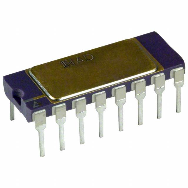
| 产品图片 |
|
| rohs | 否不符合限制有害物质指令(RoHS)规范要求 |
| 产品系列 | 放大器 IC,精密放大器,Analog Devices AD825AR- |
| 数据手册 | |
| 产品型号 | AD825AR |
| PCN过时产品 | |
| 产品培训模块 | http://www.digikey.cn/PTM/IndividualPTM.page?site=cn&lang=zhs&ptm=30008http://www.digikey.cn/PTM/IndividualPTM.page?site=cn&lang=zhs&ptm=26202 |
| 产品目录页面 | |
| 产品种类 | 精密放大器 |
| 供应商器件封装 | 8-SOIC N |
| 共模抑制比—最小值 | 80 dB |
| 关闭 | No |
| 包装 | 管件 |
| 压摆率 | 140 V/µs |
| 双重电源电压 | +/- 9 V, +/- 12 V, +/- 15 V |
| 商标 | Analog Devices |
| 增益带宽生成 | 30 MHz |
| 增益带宽积 | 26MHz |
| 安装类型 | 表面贴装 |
| 安装风格 | SMD/SMT |
| 封装 | Tube |
| 封装/外壳 | 8-SOIC(0.154",3.90mm 宽) |
| 封装/箱体 | SOIC-8 |
| 工作温度 | -40°C ~ 85°C |
| 工作电源电压 | 10 V to 36 V |
| 工厂包装数量 | 98 |
| 放大器类型 | J-FET |
| 最大双重电源电压 | +/- 18 V |
| 最大工作温度 | + 85 C |
| 最小双重电源电压 | +/- 5 V |
| 最小工作温度 | - 40 C |
| 标准包装 | 98 |
| 电压-电源,单/双 (±) | 10 V ~ 36 V, ±5 V ~ 18 V |
| 电压-输入失调 | 1mV |
| 电压增益dB | 66 dB |
| 电流-电源 | 6.5mA |
| 电流-输入偏置 | 15pA |
| 电流-输出/通道 | 50mA |
| 电源电压-最大 | 36 V |
| 电源电压-最小 | 10 V |
| 电源电流 | 7.2 mA |
| 电源类型 | Dual |
| 电路数 | 1 |
| 系列 | AD825 |
| 视频文件 | http://www.digikey.cn/classic/video.aspx?PlayerID=1364138032001&width=640&height=505&videoID=2245193153001http://www.digikey.cn/classic/video.aspx?PlayerID=1364138032001&width=640&height=505&videoID=2245193159001 |
| 转换速度 | 130 V/us at +/- 5 V |
| 输入偏压电流—最大 | 4 pA |
| 输入补偿电压 | 1 mV |
| 输出类型 | No |
| 通道数量 | 1 Channel |


- 商务部:美国ITC正式对集成电路等产品启动337调查
- 曝三星4nm工艺存在良率问题 高通将骁龙8 Gen1或转产台积电
- 太阳诱电将投资9.5亿元在常州建新厂生产MLCC 预计2023年完工
- 英特尔发布欧洲新工厂建设计划 深化IDM 2.0 战略
- 台积电先进制程称霸业界 有大客户加持明年业绩稳了
- 达到5530亿美元!SIA预计今年全球半导体销售额将创下新高
- 英特尔拟将自动驾驶子公司Mobileye上市 估值或超500亿美元
- 三星加码芯片和SET,合并消费电子和移动部门,撤换高东真等 CEO
- 三星电子宣布重大人事变动 还合并消费电子和移动部门
- 海关总署:前11个月进口集成电路产品价值2.52万亿元 增长14.8%


PDF Datasheet 数据手册内容提取
Low Cost, General-Purpose High Speed JFET Amplifier Data Sheet AD825 FEATURES CONNECTION DIAGRAMS High speed NC 1 8 NC 41 MHz, −3 dB bandwidth –IN 2 AD825 7 +VS 125 V/µs slew rate +IN 3 TOP VIEW 6 OUTPUT Inp8u0t n bsi ases tctulirnrge ntitm oef 20 pA and noise current of 10 fA/√Hz –VS N4C( =N oNtO to C SOcNaNleE)CT5 NC 00876-E-001 Input voltage noise of 12 nV/√Hz Figure 1. 8-Lead Plastic SOIC (R-8) Package Fully specified power supplies: ±5 V to ±15 V Low distortion: −76 dB at 1 MHz NC 1 16 NC High output drive capability NC 2 15 NC Drives unlimited capacitance load NC 3 14 NC 50 mA min output current –INPUT 4 AD825 13 +VS TOP VIEW No phase reversal when input is at rail +INPUT 5 (Not to Scale) 12 OUTPUT Available in 8-lead SOIC –VS 6 11 NC NC 7 10 NC ACCPDPsL ICATIONS NC N8C = NO CONNECT9 NC 00876-E-002 Low distortion filters Figure 2. 16-Lead Plastic SOIC (RW-16) Package Mixed gain stages Audio amplifiers Photo detector interfaces ADC input buffers DAC output buffers GENERAL DESCRIPTION The AD825 is a superbly optimized operational amplifier for 10V 200ns high speed, low cost, and dc parameters, making it ideally suited for a broad range of signal conditioning and data acquisition applications. The ac performance, gain, bandwidth, slew rate, and drive capability are all very stable over temperature. The AD825 also maintains stable gain under varying load conditions. The unique input stage has ultralow input bias current and input current noise. Signals that go to either rail on this high performance input do not cause phase reversals at the output. TMhUesXe ofeuattpuurtess, mcreaaktei nthge m AinDi8m2a5l ao fgfoseotd a cnhdo gicaein a se rar obrusf.f er for 10V 00876-E-003 The AD825 is fully specified for operation with dual ±5 V and Figure 3. Performance with Rail-to-Rail Input Signals ±15 V supplies. This power supply flexibility, and the low supply current of 6.5 mA with excellent ac characteristics under all supply conditions, makes the AD825 well-suited for many demanding applications. Rev. G Document Feedback Information furnished by Analog Devices is believed to be accurate and reliable. However, no responsibility is assumed by Analog Devices for its use, nor for any infringements of patents or other One Technology Way, P.O. Box 9106, Norwood, MA 02062-9106, U.S.A. rights of third parties that may result from its use. Specifications subject to change without notice. No license is granted by implication or otherwise under any patent or patent rights of Analog Devices. Tel: 781.329.4700 ©2014 Analog Devices, Inc. All rights reserved. Trademarks and registered trademarks are the property of their respective owners. Technical Support www.analog.com
AD825 Data Sheet TABLE OF CONTENTS Features .............................................................................................. 1 Typical Performance Characteristics ..............................................6 Applications ....................................................................................... 1 Driving Capacitive Loads .............................................................. 10 Connection Diagrams ...................................................................... 1 Theory of Operation ...................................................................... 10 General Description ......................................................................... 1 Input Consideration ................................................................... 10 Revision History ............................................................................... 2 Grounding and Bypassing ......................................................... 10 Specifications ..................................................................................... 3 Second-Order Low-Pass Filter ................................................. 11 Absolute Maximum Ratings ............................................................ 5 Outline Dimensions ....................................................................... 12 Pin Configurations ........................................................................... 5 Ordering Guide .......................................................................... 12 ESD Caution .................................................................................. 5 REVISION HISTORY 4/14—Rev. F to Rev. G 2/01—Data Sheet Changed from Rev. C to Rev. D Updated Outline Dimensions ....................................................... 12 Addition of 16-lead SOIC package (R-16) Changes to Ordering Guide .......................................................... 12 Connection Diagram ........................................................................ 4 Addition to Absolute Maximum Ratings ....................................... 4 10/04—Data Sheet Changed from Rev. E to Rev. F Addition to Ordering Guide (R-16) ................................................ 4 Changes to Figure 1 .......................................................................... 1 Addition of 16-lead SOIC package (R-16) Changes to Figure 4 .......................................................................... 5 Outline Dimensions ....................................................................... 11 Changes to Figure 21 ........................................................................ 8 3/04—Data Sheet Changed from Rev. D to Rev. E Changes to Specifications ................................................................ 3 Addition of 16-Lead SOIC Pin Configuration ............................. 5 Changes to Figure 27 ........................................................................ 9 Updated Outline Dimensions ....................................................... 12 Updated Ordering Guide ............................................................... 12 Rev. G | Page 2 of 12
Data Sheet AD825 SPECIFICATIONS All limits are determined to be at least four standard deviations away from mean value. At T = 25°C, V = ±15 V, unless otherwise noted. A S Table 1. AD825A Parameter Conditions V Min Typ Max Unit S DYNAMIC PERFORMANCE Unity Gain Bandwidth ±15 V 23 26 MHz Bandwidth for 0.1 dB Flatness Gain = +1 ±15 V 18 21 MHz −3 dB Bandwidth Gain = +1 ±15 V 44 46 MHz Slew Rate R = 1 kΩ, G = +1 ±15 V 125 140 V/µs LOAD Settling Time to 0.1% 0 V to 10 V Step, A = −1 ±15 V 150 180 ns V to 0.1% 0 V to 10 V Step, A = −1 ±15 V 180 220 ns V Total Harmonic Distortion F = 1 MHz, G = −1 ±15 V −77 dB C Differential Gain Error NTSC ±15 V 1.3 % (R = 150 Ω) Gain = +2 LOAD Differential Phase Error NTSC ±15 V 2.1 Degrees (R = 150 Ω) Gain = +2 LOAD INPUT OFFSET VOLTAGE ±15 V 1 2 mV T to T 5 mV MIN MAX Offset Drift 10 µV/°C INPUT BIAS CURRENT ±15 V 15 40 pA T 5 pA MIN T 700 pA MAX INPUT OFFSET CURRENT ±15 V 20 30 pA T 5 pA MIN T 440 pA MAX OPEN-LOOP GAIN V = ±10 V ±15 V OUT R = 1 kΩ 70 76 dB LOAD V = ±7.5 V ±15 V OUT R = 1 kΩ 70 76 dB LOAD V = ±7.5 V ±15 V OUT R = 150 kΩ (50 mA Output) 68 74 dB LOAD COMMON-MODE REJECTION V = ±10 ±15 V 71 80 dB CM INPUT VOLTAGE NOISE f = 10 kHz ±15 V 12 nV/√Hz INPUT CURRENT NOISE f = 10 kHz ±15 V 10 fA/√Hz INPUT COMMON-MODE VOLTAGE RANGE ±15 V ±13.5 V OUTPUT VOLTAGE SWING R = 1 kΩ ±15 V 13 ±13.3 V LOAD R = 500 Ω ±15 V 12.9 ±13.2 V LOAD Output Current ±15 V 50 mA Short-Circuit Current ±15 V 100 mA INPUT RESISTANCE 5 ×10¹¹ Ω INPUT CAPACITANCE 6 pF OUTPUT RESISTANCE Open Loop 8 Ω POWER SUPPLY Quiescent Current ±15 V 6.5 7.2 mA T to T ±15 V 7.5 mA MIN MAX Rev. G | Page 3 of 12
AD825 Data Sheet All limits are determined to be at least four standard deviations away from mean value. At T = 25°C, V = ±5 V unless otherwise noted. A S Table 2. AD825A Parameter Conditions V Min Typ Max Unit S DYNAMIC PERFORMANCE Unity Gain Bandwidth ±5 V 18 21 MHz Bandwidth for 0.1 dB Flatness Gain = +1 ±5 V 8 10 MHz −3 dB Bandwidth Gain = +1 ±5 V 34 37 MHz Slew Rate R = 1 kΩ, G = −1 ±5 V 115 130 V/µs LOAD Settling Time to 0.1% −2.5 V to +2.5 V ±5 V 75 90 ns to 0.01% −2.5 V to +2.5 V ±5 V 90 110 ns Total Harmonic Distortion F = 1 MHz, G = −1 ±5 V −76 dB C Differential Gain Error NTSC ±5 V 1.2 % (R = 150 Ω) Gain = +2 LOAD Differential Phase Error NTSC ±5 V 1.4 Degrees (R = 150 Ω) Gain = +2 LOAD INPUT OFFSET VOLTAGE ±5 V 1 2 mV T to T 5 mV MIN MAX Offset Drift 10 µV/°C INPUT BIAS CURRENT ±5 V 10 30 pA T 5 pA MIN T 600 pA MAX INPUT OFFSET CURRENT ±5 V 15 25 pA T 5 pA MIN Offset Current Drift T 280 pA MAX OPEN-LOOP GAIN V = ±2.5 ±5 V OUT R = 500 Ω 64 66 dB LOAD R = 150 Ω 64 66 dB LOAD COMMON-MODE REJECTION V = ±2 V ±5 V 69 80 dB CM INPUT VOLTAGE NOISE f = 10 kHz ±5 V 12 nV/√Hz INPUT CURRENT NOISE f = 10 kHz ±5 V 10 fA/√Hz INPUT COMMON-MODE VOLTAGE RANGE ±5 V ± 3.5 V OUTPUT VOLTAGE SWING R = 500 Ω +3.2 ±3.4 V LOAD R = 150 Ω ±5 V +3.1 ±3.2 V LOAD Output Current ±5 V 50 mA Short-Circuit Current 80 mA INPUT RESISTANCE 5 ×10¹¹ Ω INPUT CAPACITANCE 6 pF OUTPUT RESISTANCE Open Loop 8 Ω POWER SUPPLY Quiescent Current ±5 V 6.2 6.8 mA T to T ±5 V 7.5 mA MIN MAX POWER SUPPLY REJECTION V = ±5 V to ±15 V 76 88 dB S Rev. G | Page 4 of 12
Data Sheet AD825 ABSOLUTE MAXIMUM RATINGS PIN CONFIGURATIONS Table 3. Parameter Rating NC 1 8 NC Supply Voltage ±18 V –IN 2 AD825 7 +VS Internal Power Dissipation1 +IN 3 TOP VIEW 6 OUTPUT InpSumt aVlol Oltaugtlein (eC o(Rm) mon Mode) ±SeVeS Figure 6 –VS N4C( =N oNtO to C SOcNaNleE)CT5 NC 00876-E-001 Differential Input Voltage ±VS Figure 4. 8-Lead SOIC Output Short-Circuit Duration See Figure 6 Storage Temperature Range (R-8, RW-16) −65°C to +125°C Operating Temperature Range −40°C to +85°C NC 1 16 NC Lead Temperature Range 300°C NC 2 15 NC (Soldering 10 sec) NC 3 14 NC –INPUT 4 AD825 13 +VS 1 Specification is for device in free air: +INPUT 5 (NToOt Pto V SIEcaWle) 12 OUTPUT 8-lead SOIC package: θJA = 155°C/W –VS 6 11 NC 16-lead SOIC package: θJA = 85°C/W NC 7 10 NC Smtraeys sceasu saeb opveer mthaonseen lti sdteadm uanged etor Athbes odleuvtiec eM. Taxhiims iusm a sRtraetsins gs NC N8C = NO CONNECT9 NC 00876-E-002 rating only; functional operation of the device at these or any Figure 5. 16-Lead SOIC other conditions above those indicated in the operational section of this specification is not implied. Exposure to absolute maximum rating conditions for extended periods may affect 2.5 device reliability. W) TJ = 150°C N (2.0 O 16-LEAD SOIC PACKAGE TI A P SSI1.5 DI R E W O1.0 P M U M AXI0.5 8-LEAD SOIC PACKAGE M 0–50–40–30–20A–M10BIE0NT 1T0EM2P0ER3A0TU4R0E (5°C0)60 70 80 90 00876-E-004 Figure 6. Maximum Power Dissipation vs. Temperature ESD CAUTION Rev. G | Page 5 of 12
AD825 TYPICAL PERFORMANCE CHARACTERISTICS 20 100 15 10 ) 10 V) E ( G ( 5 NC N A SWI 0 RL = 150 RL = 1k PED 1 T M PU T I UT –5 PU O T U –10 O0.1 –15 –200 2 4 6SUPPL8Y VOLT10AGE (1V2) 14 16 18 00876-E-005 0.01100 1k F1R0EkQUENCY1 (0H0zk) 1M 10M 00876-E-008 Figure 7. Output Voltage Swing vs. Supply Voltage Figure 10. Closed-Loop Output Impedance vs. Frequency 15 35 80 30 BANDWIDTH 10 VS =±15V MHz) WING (V) 5 DWIDTH (2250 60 RGIN (°C) PUT S 0 VS =±5V N BAN15 PHASE MARGIN SE MA OUT–5 VS =±15V NITY GAI10 40 PHA U –10 5 –150 100 200 300LOA4D0 0RES5I0S0TAN6C00E (7)00 800 900 1000 00876-E-006 0–60 –40 –20 0 TE2M0PERA40TURE6 0(°C) 80 100 120 14020 00876-E-009 Figure 8. Output Voltage Swing vs. Load Resistance Figure 11. Unity Gain Bandwidth and Phase Margin vs. Temperature 7.0 80 180 VS =±15V –40° 70 135 +25° mA)6.5 +85° dB)60 VS =±5V 90 grees) T ( N (50 45 De REN GAI SE ( UR6.0 OP 40 0 HA C O P SUPPLY 5.5 OPEN-L3200 EN-LOOP P O 10 5.00 2 4 6SUPP8LY VO10LTAG1E2 (±V)14 16 18 20 00876-E-007 01k 10k F1R00EkQUENCY 1(HMz) 10M 100M 00876-E-010 Figure 9. Quiescent Supply Current vs. Supply Voltage Figure 12. Open-Loop Gain and Phase Margin vs. Frequency for Various Temperatures Rev. F | Page 6 of 12
AD825 80 30 RL = 1k 75 p) B) p- AIN (d VS =±15V GE (V 20 G A OP 70 OLT RL = 150 O V N-L UT PE VS =±5V TP10 O U 65 O 6010 LOAD RES1ISkTANCE () 10k 00876-E-011 100k 100k FREQUENCY (1HMz) 10M 00876-E-014 Figure 13. Open-Loop Gain vs. Load Resistance Figure 16. Large Signal Frequency Response; G = +2 10 200 0 180 –10 160 –PSRR –20 s)140 n PSR (dB)–––345000 +PSRR TLING TIME (11028000 00..011%% 00.0.11%% T E –60 S 60 –70 40 –80 20 –9010k 100kFREQUENCY (1HMz) 10M 00876-E-012 010 8 6 4OUTP2UT SW0ING (0– 2to±V–)4 –6 –8 –10 00876-E-015 Figure 14. Power Supply Rejection vs. Frequency Figure 17. Output Swing and Error vs. Settling Time 130 –50 120 –55 110 100 –60 VS =±15V B) SECOND B)90 N (d–65 d O MR (80 VS =±5V RTI THIRD C70 TO–70 S DI 60 –75 50 –80 40 3010 100 1kFREQU1E0NkCY (Hz1)00k 1M 10M 00876-E-013 –81500k FREQUE1MNCY (Hz) 10M 00876-E-016 Figure 15. Common-Mode Rejection vs. Frequency Figure 18. Harmonic Distortion vs. Frequency Rev. F | Page 7 of 12
AD825 160 +VS 10F ±15V 140 0.01F E (V/s) 112000 ±5V FHGUPNE PNCUETOLIRORSANET ((OLSRSS)) VIN 32 AD82745 0.601VOFUT TPE6PK2RT0OR4 BOFENETIX TEPKR7TEARA2OM4NPIX LEW RAT 8600 50 –VS 10F RL 00876-E-020 S Figure 22. Noninverting Amplifier Connection 40 20 0–60 –40 –20 0 TE2M0PERA40TURE6 0(°C) 80 100 120 140 00876-E-017 Figure 19. Slew Rate vs. Temperature 2 5V 100ns 1 0 –1 B)–2 d N (–3 AI G–4 VIN VOUT –5 VS 0.1dB FLATNESS ±5V 10MHz –6 ±15V 21MHz ––781k 10k FR1E00QkUENCY (Hz1)M 10M 00876-E-018 5V 00876-E-021 Figure 20. Closed-Loop Gain vs. Frequency, Gain = +1 Figure 23. Noninverting Large Signal Pulse Response, RL = 1 kΩ 2 200mV 50ns 1 0 –1 B)–2 N (d–3 VIN 1k 1k AI G –4 VOUT –5 –6 VS 0.1dB FLATNESS ––781k ±±155VV1790..k78MMHHzz FR1E00QkUENCY (Hz1)M 10M 00876-E-019 200mV 00876-E-022 Figure 21. Closed-Loop Gain vs. Frequency, Gain = −1 Figure 24. Noninverting Small Signal Pulse Response, RL = 1 kΩ Rev. F | Page 8 of 12
AD825 5V 100ns 5V 100ns 5V 00876-E-023 5V 00876-E-026 Figure 25. Noninverting Large Signal Pulse Response, RL = 150 Ω Figure 28. Inverting Large Signal Pulse Response, RL = 1 kΩ 200mV 50ns 200mV 50ns 200mV 00876-E-024 200mV 00876-E-027 Figure 26. Noninverting Small Signal Pulse Response, RL = 150 Ω Figure 29. Inverting Small Signal Pulse Response, RL = 1 kΩ 1k +VS 10F 0.01F HP PULSE VIN 7 GENERATOR 1RkIN 32 AD825 6 VOUT TPE6PK2RT0OR4 BOFENETIX TEPKR7TEARA2O4MNPIX 4 50 –VS 01.001FF RL 00876-E-025 Figure 27. Inverting Amplifier Connection Rev. F | Page 9 of 12
AD825 Data Sheet DRIVING CAPACITIVE LOADS The internal compensation of the AD825, together with its high VPOS output current drive, permits excellent large signal performance while driving extremely high capacitive loads. 1kΩ NEG +VS 10µF POS 0.01µF HP PULSE VIN 7 CF VOUT GENERATOR 1RkIΩN 23 AD825 6 VOUT TPE6PK2RT0OR4 BOFENETIX TEPKR7TEARA2O4MNPIX 4 Figure5 30Ω0. Invertin–gV SAm0p1.l00if1µiµeFFr DrivingC aL Capacitive Load 00876-E-028 VNEG 00876-E-030 Figure 32. Simplified Schematic 5V 500ns INPUT The capacitor, C, in the output stage, enables the AD825 to F drive heavy capacitive loads. For light loads, the gain of the output buffer is close to unity, C is bootstrapped, and not much F happens. As the capacitive load is increased, the gain of the output buffer is decreased and the bandwidth of the amplifier is reduced through a portion of C adding to the dominant pole. F As the capacitive load is further increased, the amplifier’s bandwidth continues to drop, maintaining the stability of the AD825. OUTPUT 5V 00876-E-029 ITNhPe UADT 8C2O5 wNiSthI DitsE uRnAiqTuIeO inNp ut stage ensures no phase Figure 31. Inverting Amplifier Pulse Response While Driving a 400 pF Capacitive Load reversal for signals as large as or even larger than the supply voltages. Also, layout considerations of the input transistors THEORY OF OPERATION ensure functionality even with a large differential signal. The AD825 is a low cost, wideband, high performance FET The need for a low noise input stage calls for a larger FET input operational amplifier. With its unique input stage design, transistor. One should consider the additional capacitance that the AD825 ensures no phase reversal, even for inputs that is added to ensure stability. When filters are designed with the exceed the power supply voltages, and its output stage is AD825, one needs to consider the input capacitance (5 pF to designed to drive heavy capacitive or resistive loads with small 6 pF) of the AD825 as part of the passive network. changes relative to no load conditions. GROUNDING AND BYPASSING The AD825 (Figure 32) consists of common-drain, common- The AD825 is a low input bias current FET amplifier. Its high base FET input stage driving a cascoded, common-base frequency response makes it useful in applications, such as matched NPN gain stage. The output buffer stage uses emitter photodiode interfaces, filters, and audio circuits. When followers in a Class AB amplifier that can deliver large current designing high frequency circuits, some special precautions are to the load while maintaining low levels of distortion. in order. Circuits must be built with short interconnects, and resistances should have low inductive paths to ground. Power supply leads should be bypassed to common as close as possible to the amplifier pins. Ceramic capacitors of 0.1 µF are recommended. Rev. G | Page 10 of 12
Data Sheet AD825 SECOND-ORDER LOW-PASS FILTER +5V C1 A second-order Butterworth low-pass filter can be implemented 24pF C3 0.1µF R1 R2 using the AD825 as shown in Figure 33. The extremely low bias 9.31kΩ 9.31kΩ currents of the AD825 allow the use of large resistor values and, VIN C2 AD825 VOUT 6pF consequently, small capacitor values without concern for developing large offset errors. Low current noise is another factor in permitting the use of large resistors without having to wWoirthry t habe ovuatl uthese srheosuwlnta,n tth ve oclotargnee rn foriesqeu. ency will be 1 MHz. –5V0.C14µF 00876-E-031 The equations for component selection are shown below. Note Figure 33. Second-Order Butterworth Low-Pass Filter that the noninverting input (and the inverting input) has an input capacitance of 6 pF. As a result, the calculated value of C1 0 (12 pF) is reduced to 6 pF. N (dB)–10 C1= 1.414 CTIO–20 2π f R1 E CUTOFF EJ–30 R C2(farads)= 0.707 NCY –40 2π fCUTOFFR1 QUE–50 R1=R2=UserSelected(Typically10kΩto100kΩ) FRE–60 H G–70 A plot of the filter frequency response is shown in Figure 34; HI –80 b etter than 40 dB of high frequency rejection is provided. 10k 100k FREQUE1MNCY (Hz) 10M 100M 00876-E-032 Figure 34. Frequency Response of Second-Order Butterworth Filter Rev. G | Page 11 of 12
AD825 Data Sheet OUTLINE DIMENSIONS 5.00(0.1968) 4.80(0.1890) 8 5 4.00(0.1574) 6.20(0.2441) 3.80(0.1497) 1 4 5.80(0.2284) 1.27(0.0500) 0.50(0.0196) BSC 1.75(0.0688) 0.25(0.0099) 45° 0.25(0.0098) 1.35(0.0532) 8° 0.10(0.0040) 0° COPLANARITY 0.51(0.0201) 0.10 SEATING 0.31(0.0122) 0.25(0.0098) 10..2470((00..00510507)) PLANE 0.17(0.0067) COMPLIANTTOJEDECSTANDARDSMS-012-AA C(RINOEFNPEATRRREOENNLCLTEIHNEOGSNDELISYM)AEANNRDSEIAORRNOESUNANORDETEDAIN-POMPFRIFLOLMPIMIRLELIATIMTEEERTFSEO;RIRNECUQHSUEDIVIINMAELDENENSSTIIOGSNNFS.OR 012407-A Figure 35. 8-Lead Standard Small Outline Package [SOIC] Narrow Body (R-8) Dimensions shown in millimeters (inches) 10.50(0.4134) 10.10(0.3976) 16 9 7.60(0.2992) 7.40(0.2913) 1 8 10.65(0.4193) 10.00(0.3937) 1.27(0.0500) 0.75(0.0295) BSC 2.65(0.1043) 0.25(0.0098) 45° 0.30(0.0118) 2.35(0.0925) 8° 0.10(0.0039) 0° COPLANARITY 0.10 0.51(0.0201) SPLEAATNIENG 0.33(0.0130) 1.27(0.0500) 0.31(0.0122) 0.20(0.0079) 0.40(0.0157) C(RINOEFNPEATRRREOENNLCLTEIHNCEOGOSNDMELISPYM)LAEAIANNRNDSETIAORTRNOOESUJNANEORDDETEEDAICN-POSMPFTRIFALONLMPIDMIRLAELIRATIMTDEEESRTFSMEO;SRIRN-0ECU1QH3SU-EADIVAIINMAELDENENSSTIIOGSNNFS.OR 03-27-2007-B Figure 36. 16-Lead Standard Small Outline Package [SOIC_W] Wide Body (RW-16) Dimensions shown in millimeters (inches) ORDERING GUIDE Model1 Temperature Range Package Description Package Option AD825ARZ −40°C to +85°C 8-Lead SOIC_N R-8 AD825ARZ-REEL −40°C to +85°C 8-Lead SOIC_N, 13" Tape and Reel R-8 AD825ARZ-REEL7 −40°C to +85°C 8-Lead SOIC_N, 7" Tape and Reel R-8 AD825ARZ-16 −40°C to +85°C 16-Lead SOIC_W RW-16 AD825ARZ-16-REEL −40°C to +85°C 16-Lead SOIC_W, 13" Tape and Reel RW-16 AD825ARZ-16-REEL7 −40°C to +85°C 16-Lead SOIC_W, 7" Tape and Reel RW-16 AD825AR-EBZ Evaluation Board AD825ACHIPS Die 1 Z = RoHS Compliant Part. ©2014 Analog Devices, Inc. All rights reserved. Trademarks and registered trademarks are the property of their respective owners. D00876-0-4/14(G) Rev. G | Page 12 of 12
Mouser Electronics Authorized Distributor Click to View Pricing, Inventory, Delivery & Lifecycle Information: A nalog Devices Inc.: AD825AR AD825AR-16-REEL AD825AR-16-REEL7 AD825AR-REEL