ICGOO在线商城 > 集成电路(IC) > 线性 - 放大器 - 仪表,运算放大器,缓冲器放大器 > AD8253ARMZ-R7

 Datasheet下载
- 型号: AD8253ARMZ-R7
- 制造商: Analog
- 库位|库存: xxxx|xxxx
- 要求:
| 数量阶梯 | 香港交货 | 国内含税 |
| +xxxx | $xxxx | ¥xxxx |
查看当月历史价格
查看今年历史价格
AD8253ARMZ-R7产品简介:
ICGOO电子元器件商城为您提供AD8253ARMZ-R7由Analog设计生产,在icgoo商城现货销售,并且可以通过原厂、代理商等渠道进行代购。 AD8253ARMZ-R7价格参考¥67.51-¥73.60。AnalogAD8253ARMZ-R7封装/规格:线性 - 放大器 - 仪表,运算放大器,缓冲器放大器, Instrumentation Amplifier 1 Circuit 10-MSOP。您可以下载AD8253ARMZ-R7参考资料、Datasheet数据手册功能说明书,资料中有AD8253ARMZ-R7 详细功能的应用电路图电压和使用方法及教程。
| 参数 | 数值 |
| -3db带宽 | 10MHz |
| 产品目录 | 集成电路 (IC)半导体 |
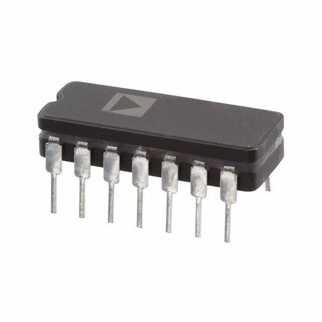
| 描述 | IC OPAMP INSTR 10MHZ 10MSOP仪表放大器 Programmable Gain Hi Speed IC |
| 产品分类 | Linear - Amplifiers - Instrumentation, OP Amps, Buffer Amps集成电路 - IC |
| 品牌 | Analog Devices |
| 产品手册 | |
| 产品图片 |
|
| rohs | 符合RoHS无铅 / 符合限制有害物质指令(RoHS)规范要求 |
| 产品系列 | 放大器 IC,仪表放大器,Analog Devices AD8253ARMZ-R7iCMOS® |
| 数据手册 | |
| 产品型号 | AD8253ARMZ-R7 |
| 产品培训模块 | http://www.digikey.cn/PTM/IndividualPTM.page?site=cn&lang=zhs&ptm=30008http://www.digikey.cn/PTM/IndividualPTM.page?site=cn&lang=zhs&ptm=26202 |
| 产品目录页面 | |
| 产品种类 | 仪表放大器 |
| 供应商器件封装 | 10-MSOP |
| 共模抑制比—最小值 | 100 dB |
| 其它名称 | AD8253ARMZ-R7CT |
| 包装 | 剪切带 (CT) |
| 压摆率 | 20 V/µs |
| 双重电源电压 | +/- 15 V |
| 可用增益调整 | 1 V/V to 1000 V/V |
| 商标 | Analog Devices |
| 增益带宽积 | - |
| 安装类型 | 表面贴装 |
| 安装风格 | SMD/SMT |
| 封装 | Reel |
| 封装/外壳 | 10-TFSOP,10-MSOP(0.118",3.00mm 宽) |
| 封装/箱体 | MSOP-10 |
| 工作温度 | -40°C ~ 85°C |
| 工作温度范围 | - 40 C to + 85 C |
| 工作电源电压 | 5 V to 15 V |
| 工厂包装数量 | 1000 |
| 带宽 | 10 MHz |
| 放大器类型 | 仪表 |
| 最大工作温度 | + 85 C |
| 最大输入电阻 | 20 kOhms at +/- 15 V |
| 最小工作温度 | - 40 C |
| 标准包装 | 1 |
| 电压-电源,单/双 (±) | ±5 V ~ 15 V |
| 电压-输入失调 | 150µV |
| 电流-电源 | 4.6mA |
| 电流-输入偏置 | 5nA |
| 电流-输出/通道 | 37mA |
| 电源电流 | 4.6 mA |
| 电路数 | 1 |
| 系列 | AD8253 |
| 视频文件 | http://www.digikey.cn/classic/video.aspx?PlayerID=1364138032001&width=640&height=505&videoID=2245193153001 |
| 转换速度 | 20 V/us |
| 输入偏压电流—最大 | 50 nA |
| 输入补偿电压 | 150 uV |
| 输出类型 | - |
| 通道数量 | 1 Channel |


PDF Datasheet 数据手册内容提取
10 MHz, 20 V/μs, G = 1, 10, 100, 1000 iCMOS Programmable Gain Instrumentation Amplifier Data Sheet AD8253 FEATURES FUNCTIONAL BLOCK DIAGRAM Small package: 10-lead MSOP DGND WR A1 A0 Programmable gains: 1, 10, 100, 1000 2 6 5 4 Digital or pin-programmable gain setting LOGIC –IN 1 Wide supply: ±5 V to ±15 V Excellent dc performance High CMRR: 100 dB (minimum), G = 100 7 OUT Low gain drift: 10 ppm/°C (maximum) Low offset drift: 1.2 μV/°C (maximum), G = 1000 Excellent ac performance +IN 10 Fast settling time: 780 ns to 0.001% (maximum) AD8253 High slew rate: 20 V/μs (minimum) LHoigwh d CisMtoRrRt ioovne: r− f1re1q0u deBn TcHy:D 1 a0t0 1 d kBH toz, 1200 VkH swz (imngin imum) +V8S –3VS RE9F 06983-001 Low noise: 10 nV/√Hz, G = 1000 (maximum) Figure 1. Low power: 4 mA 80 APPLICATIONS 70 G = 1000 60 Data acquisition Biomedical analysis 50 G = 100 Test and measurement 40 B) d GENERAL DESCRIPTION N ( 30 AI G = 10 G 20 The AD8253 is an instrumentation amplifier with digitally programmable gains that has gigaohm (GΩ) input impedance, 10 G = 1 low output noise, and low distortion, making it suitable for 0 interfacing with sensors and driving high sample rate analog-to- –10 digital converters (ADCs). It has a high bandwidth of 10 MHz, low THD of −110 dB, and –201k 10k F1R00EkQUENCY (1HMz) 10M 100M006983-023 fast settling time of 780 ns (maximum) to 0.001%. Offset drift and Figure 2. Gain vs. Frequency gain drift are guaranteed to 1.2 μV/°C and 10 ppm/°C, respectively, Table 1. Instrumentation Amplifiers by Category for G = 1000. In addition to its wide input common voltage range, General Zero Mil Low High Speed it boasts a high common-mode rejection of 100 dB at G = 1000 Purpose Drift Grade Power PGA from dc to 20 kHz. The combination of precision dc performance AD82201 AD82311 AD620 AD6271 AD8250 coupled with high speed capabilities makes the AD8253 an AD8221 AD85531 AD621 AD6231 AD8251 excellent candidate for data acquisition. Furthermore, this AD8222 AD85551 AD524 AD82231 AD8253 monolithic solution simplifies design and manufacturing and AD82241 AD85561 AD526 boosts performance of instrumentation by maintaining a tight AD8228 AD85571 AD624 match of internal resistors and amplifiers. The AD8253 user interface consists of a parallel port that allows 1 Rail-to-rail output. users to set the gain in one of two different ways (see Figure 1 The AD8253 is available in a 10-lead MSOP package and is for the functional block diagram). A 2-bit word sent via a bus specified over the −40°C to +85°C temperature range, making it can be latched using the WR input. An alternative is to use an excellent solution for applications where size and packing transparent gain mode, where the state of logic levels at the gain density are important considerations. port determines the gain. Rev. B Document Feedback Information furnished by Analog Devices is believed to be accurate and reliable. However, no responsibility is assumed by Analog Devices for its use, nor for any infringements of patents or other One Technology Way, P.O. Box 9106, Norwood, MA 02062-9106, U.S.A. rights of third parties that may result from its use. Specifications subject to change without notice. No license is granted by implication or otherwise under any patent or patent rights of Analog Devices. Tel: 781.329.4700 ©2008–2012 Analog Devices, Inc. All rights reserved. Trademarks and registered trademarks are the property of their respective owners. Technical Support www.analog.com
AD8253 Data Sheet TABLE OF CONTENTS Features .............................................................................................. 1 Power Supply Regulation and Bypassing ................................ 18 Applications ....................................................................................... 1 Input Bias Current Return Path ............................................... 18 General Description ......................................................................... 1 Input Protection ......................................................................... 18 Functional Block Diagram .............................................................. 1 Reference Terminal .................................................................... 19 Revision History ............................................................................... 2 Common-Mode Input Voltage Range ..................................... 19 Specifications ..................................................................................... 3 Layout .......................................................................................... 19 Timing Diagram ........................................................................... 5 RF Interference ........................................................................... 19 Absolute Maximum Ratings ............................................................ 6 Driving an Analog-to-Digital Converter ................................ 20 Maximum Power Dissipation ..................................................... 6 Applications Information .............................................................. 21 ESD Caution .................................................................................. 6 Differential Output .................................................................... 21 Pin Configuration and Function Descriptions ............................. 7 Setting Gains with a Microcontroller ...................................... 21 Typical Performance Characteristics ............................................. 8 Data Acquisition ......................................................................... 22 Theory of Operation ...................................................................... 16 Outline Dimensions ....................................................................... 23 Gain Selection ............................................................................. 16 Ordering Guide .......................................................................... 23 REVISION HISTORY 10/12—Rev. A to Rev. B Changed Digital Input Voltage Low Maximum Parameter from 1.2 V to 2.1 V and Changed Digital Input Voltage High Typical Parameter from 1.5 V to 2.8 V ........................................................ 4 Updated Outline Dimensions ....................................................... 23 8/08—Rev. 0 to Rev. A Changes to Ordering Guide .......................................................... 23 7/08—Revision 0: Initial Version Rev. B | Page 2 of 24
Data Sheet AD8253 SPECIFICATIONS +V = +15 V, −V = −15 V, V = 0 V @ T = 25°C, G = 1, R = 2 kΩ, unless otherwise noted. S S REF A L Table 2. Parameter Conditions Min Typ Max Unit COMMON-MODE REJECTION RATIO (CMRR) CMRR to 60 Hz with 1 kΩ Source Imbalance +IN = −IN = −10 V to +10 V G = 1 80 100 dB G = 10 96 120 dB G = 100 100 120 dB G = 1000 100 120 dB CMRR to 20 kHz1 +IN = −IN = −10 V to +10 V G = 1 80 dB G = 10 96 dB G = 100 100 dB G = 1000 100 dB NOISE Voltage Noise, 1 kHz, RTI G = 1 45 nV/√Hz G = 10 12 nV/√Hz G = 100 11 nV/√Hz G = 1000 10 nV/√Hz 0.1 Hz to 10 Hz, RTI G = 1 2.5 μV p-p G = 10 1 μV p-p G = 100 0.5 μV p-p G = 1000 0.5 μV p-p Current Noise, 1 kHz 5 pA/√Hz Current Noise, 0.1 Hz to 10 Hz 60 pA p-p VOLTAGE OFFSET Offset RTI V G = 1, 10, 100, 1000 ±150 + 900/G μV OS Over Temperature T = −40°C to +85°C ±210 + 900/G μV Average TC T = −40°C to +85°C ±1.2 + 5/G μV/°C Offset Referred to the Input vs. Supply (PSR) V = ±5 V to ±15 V ±5 + 25/G μV/V S INPUT CURRENT Input Bias Current 5 50 nA Over Temperature2 T = −40°C to +85°C 40 60 nA Average TC T = −40°C to +85°C 400 pA/°C Input Offset Current 5 40 nA Over Temperature T = −40°C to +85°C 40 nA Average TC T = −40°C to +85°C 160 pA/°C DYNAMIC RESPONSE Small-Signal −3 dB Bandwidth G = 1 10 MHz G = 10 4 MHz G = 100 550 kHz G = 1000 60 kHz Settling Time 0.01% ΔOUT = 10 V step G = 1 700 ns G = 10 680 ns G = 100 1.5 μs G = 1000 14 μs Rev. B | Page 3 of 24
AD8253 Data Sheet Parameter Conditions Min Typ Max Unit Settling Time 0.001% ΔOUT = 10 V step G = 1 780 ns G = 10 880 ns G =100 1.8 μs G = 1000 1.8 μs Slew Rate G = 1 20 V/μs G = 10 20 V/μs G = 100 12 V/μs G = 1000 2 V/μs Total Harmonic Distortion + Noise f = 1 kHz, R = 10 kΩ, ±10 V, −110 dB L G = 1, 10 Hz to 22 kHz band- pass filter GAIN Gain Range G = 1, 10, 100, 1000 1 1000 V/V Gain Error OUT = ±10 V G = 1 0.03 % G = 10, 100, 1000 0.04 % Gain Nonlinearity OUT = −10 V to +10 V G = 1 R = 10 kΩ, 2 kΩ, 600 Ω 5 ppm L G = 10 R = 10 kΩ, 2 kΩ, 600 Ω 3 ppm L G = 100 R = 10 kΩ, 2 kΩ, 600 Ω 18 ppm L G = 1000 R = 10 kΩ, 2 kΩ, 600 Ω 110 ppm L Gain vs. Temperature All gains 3 10 ppm/°C INPUT Input Impedance Differential 4||1.25 GΩpF Common Mode 1||5 GΩpF Input Operating Voltage Range V = ±5 V to ±15 V −V + 1 +V − 1.5 V S S S Over Temperature3 T = −40°C to +85°C −V + 1.2 +V − 1.7 V S S OUTPUT Output Swing −13.7 +13.6 V Over Temperature4 T = −40°C to +85°C −13.7 +13.6 V Short-Circuit Current 37 mA REFERENCE INPUT R 20 kΩ IN I +IN, −IN, REF = 0 1 μA IN Voltage Range −V +V V S S Gain to Output 1 ± 0.0001 V/V DIGITAL LOGIC Digital Ground Voltage, DGND Referred to GND −V + 4.25 0 +V − 2.7 V S S Digital Input Voltage Low Referred to GND DGND 2.1 V Digital Input Voltage High Referred to GND 2.8 +V V S Digital Input Current 1 μA Gain Switching Time5 325 ns t See Figure 3 timing diagram 15 ns SU t 30 ns HD tWR-LOW 20 ns tWR-HIGH 15 ns Rev. B | Page 4 of 24
Data Sheet AD8253 Parameter Conditions Min Typ Max Unit POWER SUPPLY Operating Range ±5 ±15 V Quiescent Current, +I 4.6 5.3 mA S Quiescent Current, −I 4.5 5.3 mA S Over Temperature T = −40°C to +85°C 6 mA TEMPERATURE RANGE Specified Performance −40 +85 °C 1 See Figure 20 for CMRR vs. frequency for more information on typical performance over frequency. 2 Input bias current over temperature: minimum at hot and maximum at cold. 3 See Figure 30 for input voltage limit vs. supply voltage and temperature. 4 See Figure 32, Figure 33, and Figure 34 for output voltage swing vs. supply voltage and temperature for various loads. 5 Add time for the output to slew and settle to calculate the total time for a gain change. TIMING DIAGRAM t t WR-HIGH WR-LOW WR t t SU HD A0, A1 06983-003 Figure 3. Timing Diagram for Latched Gain Mode (See the Timing for Latched Gain Mode Section) Rev. B | Page 5 of 24
AD8253 Data Sheet ABSOLUTE MAXIMUM RATINGS power is the voltage between the supply pins (V) times the Table 3. S quiescent current (I). Assuming the load (R) is referenced to Parameter Rating S L midsupply, the total drive power is V/2 × I , some of which is Supply Voltage ±17 V S OUT dissipated in the package and some of which is dissipated in the Power Dissipation See Figure 4 load (V × I ). Output Short-Circuit Current Indefinite1 OUT OUT Common-Mode Input Voltage ±V The difference between the total drive power and the load S Differential Input Voltage ±V power is the drive power dissipated in the package. S Digital Logic Inputs ±VS PD = Quiescent Power + (Total Drive Power − Load Power) Storage Temperature Range –65°C to +125°C Operating Temperature Range2 –40°C to +85°C P V I VS VOUT –VOUT2 Lead Temperature (Soldering 10 sec) 300°C D S S 2 RL RL Junction Temperature 140°C In single-supply operation with R referenced to −V, the worst L S θ (4-Layer JEDEC Standard Board) 112°C/W JA case is V = V/2. OUT S Package Glass Transition Temperature 140°C Airflow increases heat dissipation, effectively reducing θ . In JA 1 Assumes the load is referenced to midsupply. addition, more metal directly in contact with the package leads 2 Temperature for specified performance is −40°C to +85°C. For performance from metal traces through holes, ground, and power planes to +125°C, see the Typical Performance Characteristics section. reduces the θJA. Stresses above those listed under Absolute Maximum Ratings Figure 4 shows the maximum safe power dissipation in the may cause permanent damage to the device. This is a stress package vs. the ambient temperature on a 4-layer JEDEC rating only; functional operation of the device at these or any standard board. other conditions above those indicated in the operational 2.00 section of this specification is not implied. Exposure to absolute 1.75 maximum rating conditions for extended periods may affect W) device reliability. ON ( 1.50 TI A MAXIMUM POWER DISSIPATION SIP 1.25 S The maximum safe power dissipation in the AD8253 package is DI R 1.00 limited by the associated rise in junction temperature (TJ) on WE the die. The plastic encapsulating the die locally reaches the PO 0.75 M junction temperature. At approximately 140°C, which is the MU 0.50 glass transition temperature, the plastic changes its properties. AXI M 0.25 Even temporarily exceeding this temperature limit can change the stresses that the package exerts on the die, permanently 0 sah jiufnticntgio tnh et epmarpaemraetturrice pofe r1f4o0r°mCa fnocre a onf ethxtee AndDe8d2 p5e3r. iEoxdc ceaend ing –40 –20 0AMBIE2N0T TEM4P0ERATU60RE (°C)80 100 120 06983-004 Figure 4. Maximum Power Dissipation vs. Ambient Temperature result in changes in silicon devices, potentially causing failure. ESD CAUTION The still-air thermal properties of the package and PCB (θ ), JA the ambient temperature (T ), and the total power dissipated in A the package (P ) determine the junction temperature of the die. D The junction temperature is calculated as T T P θ J A D JA The power dissipated in the package (P ) is the sum of the D quiescent power dissipation and the power dissipated in the package due to the load drive for all outputs. The quiescent Rev. B | Page 6 of 24
Data Sheet AD8253 PIN CONFIGURATION AND FUNCTION DESCRIPTIONS –IN 1 10 +IN DGND 2 AD8253 9 REF –VS 3 TOP VIEW 8 +VS AA01 45 (Not to Scale) 76 OWURT 06983-005 Figure 5. 10-Lead MSOP (RM-10) Pin Configuration Table 4. Pin Function Descriptions Pin No. Mnemonic Description 1 −IN Inverting Input Terminal. True differential input. 2 DGND Digital Ground. 3 −V Negative Supply Terminal. S 4 A0 Gain Setting Pin (LSB). 5 A1 Gain Setting Pin (MSB). 6 WR Write Enable. 7 OUT Output Terminal. 8 +V Positive Supply Terminal. S 9 REF Reference Voltage Terminal. 10 +IN Noninverting Input Terminal. True differential input. Rev. B | Page 7 of 24
AD8253 Data Sheet TYPICAL PERFORMANCE CHARACTERISTICS T @ 25°C, +V = +15 V, −V = −15 V, R = 10 kΩ, unless otherwise noted. A S S L 210 240 180 210 S150 S180 T T NI NI F U120 F U150 O O ER ER 120 B 90 B M M NU NU 90 60 60 30 30 0 0 –60 –40 CMRR–2 (0µV/V) 0 20 06983-006 –60 –40 INPU–T2 0OFFSET0 CURREN2T0 (nA) 40 60 06983-009 Figure 6. Typical Distribution of CMRR, G = 1 Figure 9. Typical Distribution of Input Offset Current 90 180 80 150 70 S UNIT120 Hz) 60 OF V/√ 50 BER 90 SE (n 40 G = 100 G = 1 M OI NU 60 N 30 G = 10 20 30 10 0 G = 1000 –200 INPU–T10 O0FFSET VOL0TAGE, VOSI,1 R00TI (µV) 200 06983-007 01 10 F1R0E0QUENCY (1Hkz) 10k 100k06983-010 Figure 7. Typical Distribution of Offset Voltage, VOSI Figure 10. Voltage Spectral Density Noise vs. Frequency 300 250 S T NI F U200 O R BE150 M U N 100 50 0 –90 –60INPU–T3 B0IAS CU0RRENT (3n0A) 60 90 06983-008 2µV/DIV 1s/DIV 06983-011 Figure 8. Typical Distribution of Input Bias Current Figure 11. 0.1 Hz to 10 Hz RTI Voltage Noise, G = 1 Rev. B | Page 8 of 24
Data Sheet AD8253 20 V) 18 µ GE ( 16 A T L 14 O V T 12 E S FF 10 O UT 8 P N N I 6 E I G 4 N 500nV/DIV 1s/DIV 06983-012 CHA 020.01 W0A.1RM-UP TIME (Minute1s) 1006983-015 Figure 12. 0.1 Hz to 10 Hz RTI Voltage Noise, G = 1000 Figure 15. Change in Input Offset Voltage vs. Warm-Up Time, G = 1000 18 140 16 120 14 G = 1000 100 G = 100 12 SE (pA/√Hz)108 SRR (dB) 8600 G = 1 OI P G = 10 N 6 40 4 20 2 0 0 1 10 F1R0E0QUENCY (1Hkz) 10k 100k06983-013 10 100 FR1kEQUENCY 1(H0kz) 100k 1M 06983-016 Figure 13. Current Noise Spectral Density vs. Frequency Figure 16. Positive PSRR vs. Frequency, RTI 140 120 G = 100 G = 1000 100 B) 80 d RR ( G = 10 S 60 P 40 G = 1 140pA/DIV 1s/DIV 06983-014 200 10 100 FR1kEQUENCY 1(H0kz) 100k 1M 06983-017 Figure 14. 0.1 Hz to 10 Hz Current Noise Figure 17. Negative PSRR vs. Frequency, RTI Rev. B | Page 9 of 24
AD8253 Data Sheet 20 12.0 120 10 10.5 IB+ A) 100 NT (nA)–100 IB– 97..05 ENT (n 80 G = 1000 BIAS CURRE––2300 64..05 FFSET CURR CMRR (dB) 60 G = 10 G = 100 UT IOS T O 40 P U N–40 3.0 P I N I 20 G = 1 –50 1.5 –60–15 –10 COM–M5ON-MOD0E VOLTAG5E (V) 10 150 06983-018 010 100 FR1kEQUENCY 1(H0kz) 100k 1M06983-021 Figure 18. Input Bias Current and Offset Current vs. Common-Mode Voltage Figure 21. CMRR vs. Frequency, 1 kΩ Source Imbalance 30 15 25 10 D 20 ANA) ENT NT (n15 V) 5 RE V/ RR µ CUUR10 R ( 0 T BIAS FSET C 5 IB+ IB– CMR –5 UF NPO 0 I IOS –10 –5 –10–60 –40 –20 0 TEM20PERA40TURE6 0(°C) 80 100 120 140 06983-019 –15–50 –30 –10 10TEMP3E0RATU5R0E (°C7)0 90 110 13006983-022 Figure 19. Input Bias Current and Offset Current vs. Temperature Figure 22. CMRR vs. Temperature, G = 1 120 80 G = 1000 70 100 G = 100 G = 1000 60 50 80 G = 100 MRR (dB) 60 G = 1 G = 10 AIN (dB) 4300 G = 10 C G 20 40 10 G = 1 0 20 –10 010 100 FR1kEQUENCY 1(H0kz) 100k 1M06983-020 –201k 10k F1R00EkQUENCY (1HMz) 10M 100M006983-023 Figure 20. CMRR vs. Frequency Figure 23. Gain vs. Frequency Rev. B | Page 10 of 24
Data Sheet AD8253 40 400 30 300 DIV) 20 DIV) 200 m/ m/ RITY (10pp 100 RITY (10 pp 1000 EA –10 EA–100 N N NLI NLI O –20 O–200 N N –30 –300 –40–10 –8 –6 –4OUT–P2UT VO0LTAG2E (V)4 6 8 1006983-024 –400–10 –8 –6 –4OUT–P2UT V0OLTAG2E (V)4 6 8 1006983-027 Figure 24. Gain Nonlinearity, G = 1, RL = 10 kΩ, 2 kΩ, 600 Ω Figure 27. Gain Nonlinearity, G = 1000, RL = 10 kΩ, 2 kΩ, 600 Ω 40 16 0V, +13.9V 30 V) 12 VS, ±15V E ( ppm/DIV) 2100 VOLTAG 84 –14.1V, +7.3V 0V, +3.8V +13.8V, +7.3V TY (10 0 MODE 0 –4V, +1.9V VS= ±5V +3.8V, +1.9V NEARI –10 MON- –4 –4V, –1.9V +3.8V, –1.9V NONLI –20 T COM –8 –14.1V, –7.3V 0V, –4.2V +13.8V, –7.3V U P N –30 I –12 0V, –14.2V –40–10 –8 –6 –4OUT–P2UT VO0LTAG2E (V)4 6 8 1006983-025 –16–16 –12 –8 OU–T4PUT VO0LTAGE4 (V) 8 12 16 06983-028 Figure 25. Gain Nonlinearity, G = 10, RL = 10 kΩ, 2 kΩ, 600 Ω Figure 28. Input Common-Mode Voltage Range vs. Output Voltage, G = 1 80 16 0V, +13.7V m/DIV) 6400 LTAGE (V) 128 –14.4V, +6V 0VVS, +±31.58VV +14.1V, +6V pp 20 VO 4 NEARITY (10–200 MON-MODE –40 ––44..33VV,, –+22VV VS= ±5V ++44..33VV,, –+22VV NLI OM –14.4V, –6V 0V, –4.2V +14.1V, –6V NO–40 T C –8 U P N –60 I –12 0V, –14.1V –80–10 –8 –6 –4OUT–P2UT V0OLTAG2E (V)4 6 8 1006983-026 –16–16 –12 –8 OU–T4PUT VO0LTAGE4 (V) 8 12 16 06983-029 Figure 26. Gain Nonlinearity, G = 100, RL = 10 kΩ, 2 kΩ, 600 Ω Figure 29. Input Common-Mode Voltage Range vs. Output Voltage, G = 1000 Rev. B | Page 11 of 24
AD8253 Data Sheet +VS +125°C +85°C +VS –0.2 S –1 S–0.4 +125°C NPUT VOLTAGE (V)ED TO SUPPLY VOLTAGE –2 +25°C –40°C UT VOLTAGE SWING (V)ED TO SUPPLY VOLTAGE+–––0011....6800 +85°C +85°C ++2255°C°C ––4400°°CC IRR +2 –40°C +25°C TPRR+0.8 E UE EF OEF+0.6 R +1 R+0.4 +125°C +85°C +0.2 +125°C –VS4 6 S8UPPLY VO1L0TAGE (±V12S) 14 16 06983-030 –VS4 6 S8UPPLY VO1L0TAGE (±V12S) 14 16 06983-033 Figure 30. Input Voltage Limit vs. Supply Voltage, G = 1, VREF = 0 V, RL = 10 kΩ Figure 33. Output Voltage Swing vs. Supply Voltage, G =1000, RL = 10 kΩ 25 15 FAULT FAULT +25°C CONDITION CONDITION 20(OVER-DRIVEN (OVER-DRIVEN +85°C INPUT) INPUT) 10 15 G=1000 G=1000 V) NT (mA) 1050 +IN +Vs +IN AGE SWING ( 50 +125°C –40°C CURRE –5 –IN –IN UT VOLT –5 +85°C –10 –Vs TP +125°C U –15 O –10 +25°C –20 –40°C –25 –15 –10 –1 –100m D–10mIFFER–1mENTI–100µAL I–10µ/NP10µUT 100µVOLT1mAGE10m (V) 100m 1 1006983-031 100 LOAD RES1ISkTANCE (Ω) 10k06983-034 Figure 31. Fault Current Draw vs. Input Voltage, G = 1000, RL = 10 kΩ Figure 34. Output Voltage Swing vs. Load Resistance +VS +VS –0.2 –40°C –0.4 +25°C –0.4 VOLTAGE SWING (V)TO SUPPLY VOLTAGES+––––00111.....68022 +85°C–40°C+25°C+25°–C4+01°2C5°C +85°C VOLTAGE SWING (V)TO SUPPLY VOLTAGES +––––01122.....82600 ++8152°5C°C UT ED +1.0 UT ED +1.6 PR PR TR+0.8 TR +1.2 UE UE OREF++00..64 +125°C OREF +0.8 +0.2 +0.4 –VS4 6 S8UPPLY VO1L0TAGE (±V12S) 14 16 06983-032 –VS4 6 O8UTPUT CU1R0RENT (m1A2) 14 1606983-035 Figure 32. Output Voltage Swing vs. Supply Voltage, G = 1000, RL = 2 kΩ Figure 35. Output Voltage Swing vs. Output Current Rev. B | Page 12 of 24
Data Sheet AD8253 5V/DIV NO LOAD 47pF 100pF 1392nsTO 0.01% 1712nsTO 0.001% 0.002%/DIV 20mV/DIV 2µs/DIV 06983-036 TIME (µs) 2µs/DIV 06983-039 Figure 36. Small-Signal Pulse Response for Various Capacitive Loads, G = 1 Figure 39. Large-Signal Pulse Response and Settling Time, G = 100, RL = 10 kΩ 5V/DIV 5V/DIV 664nsTO 0.01% 12.88µsTO 0.01% 744nsTO 0.001% 16.64µsTO 0.001% 0.002%/DIV 0.002%/DIV TIME (µs) 2µs/DIV 06983-037 TIME (µs) 10µs/DIV 06983-040 Figure 37. Large-Signal Pulse Response and Settling Time, G = 1, RL = 10 kΩ Figure 40. Large-Signal Pulse Response and Settling Time, G = 1000, RL = 10 kΩ 5V/DIV 656nsTO 0.01% 840nsTO 0.001% 0.002%/DIV TIME (µs) 2µs/DIV 06983-038 20mV/DIV 2µs/DIV 06983-041 Figure 38. Large-Signal Pulse Response and Settling Time, Figure 41. Small-Signal Response, G = 10, RL = 10 kΩ G = 1, RL = 2 kΩ, CL = 100 Rev. B | Page 13 of 24
AD8253 Data Sheet 1400 1200 1000 SETTLEDTO 0.001% s) 800 n E ( M TI 600 SETTLEDTO 0.01% 400 20mV/DIV 2µs/DIV 06983-042 2000 2 4 6 8 ST1E0P SIZ1E2 (V) 14 16 18 2006983-045 Figure 42. Small-Signal Response, Figure 45. Settling Time vs. Step Size, G = 1, RL = 10 kΩ G = 10, RL = 2 kΩ, CL = 100 pF 1400 1200 1000 SETTLEDTO 0.001% s) 800 n ME ( SETTLEDTO 0.01% TI 600 400 20mV/DIV 20µs/DIV 06983-043 2000 2 4 6 8 ST1E0P SIZ1E2 (V) 14 16 18 2006983-046 Figure 43. Small-Signal Response, Figure 46. Settling Time vs. Step Size, G = 10, RL = 10 kΩ G = 100, RL = 2 kΩ, CL = 100 pF 2000 SETTLEDTO 0.001% 1800 1600 1400 SETTLEDTO 0.01% s)1200 n E (1000 M TI 800 600 400 20mV/DIV 20µs/DIV 06983-044 2000 2 4 6 8 ST1E0P SIZ1E2 (V) 14 16 18 2006983-047 Figure 44. Small-Signal Response, G = 1000, RL = 2 kΩ, CL = 100 pF Figure 47. Settling Time vs. Step Size, G = 100, RL = 10 kΩ Rev. B | Page 14 of 24
Data Sheet AD8253 20 0 –10 18 SETTLEDTO 0.001% –20 16 –30 14 –40 TIME (µs)11082 SETTLEDTO 0.01% THD + N (dB) –––567000 GGG = == 1 10100000 –80 6 –90 G = 1 4 –100 2 –110 0 –120 2 4 6 8 ST1E0P SIZ1E2 (V) 14 16 18 2006983-048 10 100 FR1kEQUENCY 1(H0kz) 100k 1M06983-050 Figure 48. Settling Time vs. Step Size, G = 1000, RL = 10 kΩ Figure 50. Total Harmonic Distortion vs. Frequency, 10 Hz to 500 kHz Band-Pass Filter, 2 kΩ Load 0 –10 –20 –30 –40 dB) –50 + N ( –60 G = 1000 D H –70 T G = 100 –80 –90 G = 10 –100 G = 1 –110 –12010 100 FR1kEQUENCY 1(H0kz) 100k 1M06983-049 Figure 49. Total Harmonic Distortion vs. Frequency, 10 Hz to 22 kHz Band-Pass Filter, 2 kΩ Load Rev. B | Page 15 of 24
AD8253 Data Sheet THEORY OF OPERATION +VS +VS A0 A1 2.2kΩ +VS –VS –VS 1.2kΩ –IN 10kΩ 10kΩ A1 –VS +VS DIGITAL GAIN A3 OUT CONTROL –VS +VS +VS 10kΩ 10kΩ A2 REF 1.2kΩ +IN –VS –VS +VS +VS 2.2kΩ WR DGND –VS –VS 06983-061 Figure 51. Simplified Schematic The AD8253 is a monolithic instrumentation amplifier based Transparent Gain Mode on the classic 3-op-amp topology, as shown in Figure 51. It is The easiest way to set the gain is to program it directly via a fabricated on the Analog Devices, Inc., proprietary iCMOS® logic high or logic low voltage applied to A0 and A1. Figure 52 process that provides precision linear performance and a robust shows an example of this gain setting method, referred to through- digital interface. A parallel interface allows users to digitally out the data sheet as transparent gain mode. Tie WR to the program gains of 1, 10, 100, and 1000. Gain control is achieved negative supply to engage transparent gain mode. In this mode, by switching resistors in an internal precision resistor array (as any change in voltage applied to A0 and A1 from logic low to shown in Figure 51). logic high, or vice versa, immediately results in a gain change. All internal amplifiers employ distortion cancellation circuitry Table 5 is the truth table for transparent gain mode, and Figure 52 and achieve high linearity and ultralow THD. Laser-trimmed shows the AD8253 configured in transparent gain mode. resistors allow for a maximum gain error of less than 0.03% for +15V G = 1 and a minimum CMRR of 100 dB for G = 1000. A pinout optimized for high CMRR over frequency enables the AD8253 10μF 0.1µF WR to offer a guaranteed minimum CMRR over frequency of 80 dB –15V A1 +5V at 20 kHz (G = 1). The balanced input reduces the parasitics A0 +IN +5V that in the past had adversely affected CMRR performance. G = 1000 GAIN SELECTION AD8253 REF This section describes how to configure the AD8253 for basic –IN operation. Logic low and logic high voltage limits are listed in the Specifications section. Typically, logic low is 0 V and logic DGND DGND 10μF 0.1µF high is 5 V; both voltages are measured with respect to DGND. Refer to the specifications table (Table 2) for the permissible –15V voltage range of DGND. The gain of the AD8253 can be set NOTE: using two methods: transparent gain mode and latched gain 1. IN TRANSPARENT GAIN MODE, WR IS TIED TO −VS. mshoodueld. Rbeeg uasreddle tsos opfr othvied me ao dwee, lpl-udlel-fuinpe dor v poultlal-gdeo awt nth ree Asis0t oarnsd TTSHHETEE TVGOOA LILNTO.A IGNGI CET HLHIEISGV EHEX,L RASEM OSPNUL LEAT,0 IB NAOGNT DIHN A AA10 GD AEANTINDE ROAM1F IA1N0RE0E0. 06983-051 Figure 52. Transparent Gain Mode, A0 and A1 = High, G = 1000 A1 pins. Rev. B | Page 16 of 24
Data Sheet AD8253 Table 5. Truth Table Logic Levels for Transparent Gain Mode Table 6. Truth Table Logic Levels for Latched Gain Mode WR A1 A0 Gain WR A1 A0 Gain −VS Low Low 1 High to Low Low Low Change to 1 −VS Low High 10 High to Low Low High Change to 10 −VS High Low 100 High to Low High Low Change to 100 −VS High High 1000 High to Low High High Change to 1000 Low to Low X1 X1 No change Latched Gain Mode Low to High X1 X1 No change High to High X1 X1 No change Some applications have multiple programmable devices such as multiplexers or other programmable gain instrumentation 1 X = don’t care. amplifiers on the same PCB. In such cases, devices can share a data bus. The gain of the AD8253 can be set using WR as a latch, On power-up, the AD8253 defaults to a gain of 1 when in allowing other devices to share A0 and A1. Figure 53 shows a latched gain mode. In contrast, if the AD8253 is configured in schematic using this method, known as latched gain mode. The transparent gain mode, it starts at the gain indicated by the AD8253 is in this mode when WR is held at logic high or logic voltage levels on A0 and A1 on power-up. low, typically 5 V and 0 V, respectively. The voltages on A0 and A1 Timing for Latched Gain Mode are read on the downward edge of the WR signal as it transitions In latched gain mode, logic levels at A0 and A1 must be held for from logic high to logic low. This latches in the logic levels on A0 and A1, resulting in a gain change. See the truth table listing a minimum setup time, tSU, before the downward edge of WR in Table 6 for more on these gain changes. latches in the gain. Similarly, they must be held for a minimum hold time, t , after the downward edge of WR to ensure that +15V HD WR +5V the gain is latched in correctly. After tHD, A0 and A1 may change 10μF 0.1µF WR 0V logic levels, but the gain does not change until the next downward A1 +5V A1 0V edge of WR. The minimum duration that WR can be held high A0 +5V +IN A0 0V is tWR-HIGH, and tWR-LOW is the minimum duration that WR can + G = PREVIOUS G = 1000 be held low. Digital timing specifications are listed in Table 2. STATE AD8253 The time required for a gain change is dominated by the settling REF time of the amplifier. A timing diagram is shown in Figure 54. – –IN When sharing a data bus with other devices, logic levels applied DGND DGND to those devices can potentially feed through to the output of 10μF 0.1µF the AD8253. Feedthrough can be minimized by decreasing the edge rate of the logic signals. Furthermore, careful layout of the –15V PCB also reduces coupling between the digital and analog NOTE: 1. ON THE DOWNWARD EDGE OF WR, AS IT TRANSITIONS portions of the board. FAGRNAODIN MA C 1LH OAARGNEIGC RE HE. IIAGNDH T ATHNOISD LE LOXAGATIMCCP HLLEOEDW, IT,N HT, EHR EEG SVAUOINLL TSTIWANGGITE ICNSH AOENS TAO0 G = 1000. 06983-052 Figure 53. Latched Gain Mode, G = 1000 t t WR-HIGH WR-LOW WR t t SU HD A0, A1 06983-053 Figure 54. Timing Diagram for Latched Gain Mode Rev. B | Page 17 of 24
AD8253 Data Sheet POWER SUPPLY REGULATION AND BYPASSING INCORRECT CORRECT The AD8253 has high PSRR. However, for optimal performance, +VS +VS a stable dc voltage should be used to power the instrumentation amplifier. Noise on the supply pins can adversely affect per- formance. As in all linear circuits, bypass capacitors must be AD8253 AD8253 used to decouple the amplifier. REF REF Place a 0.1 μF capacitor close to each supply pin. A 10 μF tantalum capacitor can be used farther away from the part (see Figure 55) –VS –VS and, in most cases, it can be shared by other precision integrated TRANSFORMER TRANSFORMER circuits. +VS +VS +VS 0.1µF 10µF WR A1 AD8253 AD8253 A0 +IN REF REF AD8253 VOUT 10MΩ LOAD –VS –VS –IN REF THERMOCOUPLE THERMOCOUPLE DGND +VS +VS 0.1µF 10µF DGND –VS 06983-054 C C Figure 55. Supply Decoupling, REF, and Output Referred to Ground AD8253 fHIGH-PASS =2π1RC R AD8253 C C INPUT BIAS CURRENT RETURN PATH REF REF The AD8253 input bias current must have a return path to its R lcoacnanl oatn parloogv igdreo au nredt.u Wrnh ceunr rthene ts poautrhc,e o, snuec shh aosu ald t hbeer cmreoactoedu ple, CAPACITIVE–LVYS COUPLED CAPACITIVELY COUP–LVESD 06983-055 (see Figure 56). Figure 56. Creating an IBIAS Path INPUT PROTECTION All terminals of the AD8253 are protected against ESD. An external resistor should be used in series with each of the inputs to limit current for voltages greater than 0.5 V beyond either supply rail. In such a case, the AD8253 safely handles a continuous 6 mA current at room temperature. For applications where the AD8253 encounters extreme overload voltages, external series resistors and low leakage diode clamps such as BAV199Ls, FJH1100s, or SP720s should be used. Rev. B | Page 18 of 24
Data Sheet AD8253 REFERENCE TERMINAL Coupling Noise The reference terminal, REF, is at one end of a 10 kΩ resistor To prevent coupling noise onto the AD8253, follow these (see Figure 51). The instrumentation amplifier output is guidelines: referenced to the voltage on the REF terminal; this is useful Do not run digital lines under the device. when the output signal needs to be offset to voltages other than Run the analog ground plane under the AD8253. its local analog ground. For example, a voltage source can be Shield fast-switching signals with digital ground to avoid tied to the REF pin to level shift the output so that the AD8253 radiating noise to other sections of the board, and never can interface with a single-supply ADC. The allowable reference run them near analog signal paths. voltage range is a function of the gain, common-mode input, Avoid crossover of digital and analog signals. and supply voltages. The REF pin should not exceed either +V S Connect digital and analog ground at one point only or −V by more than 0.5 V. S (typically under the ADC). For best performance, especially in cases where the output is Power supply lines should use large traces to ensure a low not measured with respect to the REF terminal, source imped- impedance path. Decoupling is necessary; follow the ance to the REF terminal should be kept low because parasitic guidelines listed in the Power Supply Regulation and resistance can adversely affect CMRR and gain accuracy. Bypassing section. INCORRECT CORRECT Common-Mode Rejection The AD8253 has high CMRR over frequency, giving it greater immunity to disturbances, such as line noise and its associated AD8253 AD8253 harmonics, in contrast to typical in amps whose CMRR falls off VREF around 200 Hz. They often need common-mode filters at the VREF inputs to compensate for this shortcoming. The AD8253 is able + to reject CMRR over a greater frequency range, reducing the OP1177 – 06983-056 nCeaerdef ufol rb oinaprdu tl acyoomutm moanx-immoizdees sfyilstteermin gp.e rformance. To maintain Figure 57. Driving the Reference Pin high CMRR over frequency, lay out the input traces symmetrically. COMMON-MODE INPUT VOLTAGE RANGE Ensure that the traces maintain resistive and capacitive balance; this holds for additional PCB metal layers under the input pins The 3-op-amp architecture of the AD8253 applies gain and then and traces. Source resistance and capacitance should be placed removes the common-mode voltage. Therefore, internal nodes as close to the inputs as possible. Should a trace cross the inputs in the AD8253 experience a combination of both the gained (from another layer), it should be routed perpendicular to the signal and the common-mode signal. This combined signal can input traces. be limited by the voltage supplies even when the individual input and output signals are not. Figure 28 and Figure 29 show RF INTERFERENCE the allowable common-mode input voltage ranges for various RF rectification is often a problem when amplifiers are used in output voltages, supply voltages, and gains. applications where there are strong RF signals. The disturbance LAYOUT can appear as a small dc offset voltage. High frequency signals can be filtered with a low-pass RC network placed at the input Grounding of the instrumentation amplifier, as shown in Figure 58. The In mixed-signal circuits, low level analog signals need to be filter limits the input signal bandwidth according to the following isolated from the noisy digital environment. Designing with the relationship: AD8253 is no exception. Its supply voltages are referenced to an 1 analog ground. Its digital circuit is referenced to a digital ground. FilterFreq Although it is convenient to tie both grounds to a single ground DIFF 2πR(2C C ) D C plane, the current traveling through the ground wires and PC 1 board can cause an error. Therefore, use separate analog and FilterFreq CM 2π RC digital ground planes. Only at one point, star ground, should C analog and digital ground meet. where C ≥ 10 C . D C The output voltage of the AD8253 develops with respect to the potential on the reference terminal. Take care to tie REF to the appropriate local analog ground or to connect it to a voltage that is referenced to the local analog ground. Rev. B | Page 19 of 24
AD8253 Data Sheet +15V In this example, a 1 nF capacitor and a 49.9 Ω resistor create an antialiasing filter for the AD7612. The 1 nF capacitor also serves 0.1µF 10µF to store and deliver necessary charge to the switched capacitor CC input of the ADC. The 49.9 Ω series resistor reduces the burden R +IN of the 1 nF load from the amplifier and isolates it from the kickback current injected from the switched capacitor input of the AD7612. CD AD8253 VOUT Selecting too small a resistor improves the correlation between R REF the voltage at the output of the AD8253 and the voltage at the –IN input of the AD7612 but may destabilize the AD8253. A trade- CC off must be made between selecting a resistor small enough to 0.1µF 10µF maintain accuracy and large enough to maintain stability. –15V 06983-057 +15V Figure 58. RFI Suppression 10μF 0.1µF Values of R and CC should be chosen to minimize RFI. WRA1 +12V –12V Mismatch between the R × C at the positive input and the A0 C +IN 0.1μF 0.1μF R × C at negative input degrades the CMRR of the AD8253. C By using a value of CD that is 10 times larger than the value of AD8253 49.9Ω AD7612 CC, the effect of the mismatch is reduced and performance is REF 1nF improved. –IN +5V ADR435 DRIVING AN ANALOG-TO-DIGITAL CONVERTER DGND DGND 10μF 0.1µF An instrumentation amplifier is often used in front of an analog- taom-dpilgifiitearls c roenqvueirrtee ar tbou pffreorv tiod ed rCivMe RanR .A UDsuCa. lHly,o iwnesvtreur,m thene tlaotwio n –15V 06983-058 Figure 59. Driving an ADC output noise, low distortion, and low settle time of the AD8253 make it an excellent ADC driver. Rev. B | Page 20 of 24
Data Sheet AD8253 APPLICATIONS INFORMATION DIFFERENTIAL OUTPUT SETTING GAINS WITH A MICROCONTROLLER In certain applications, it is necessary to create a differential +15V signal. High resolution analog-to-digital converters often require a 10μF 0.1µF differential input. In other cases, transmission over a long distance WR can require differential signals for better immunity to interference. A1 MICRO- CONTROLLER A0 +IN Figure 61 shows how to configure the AD8253 to output a + differential signal. An op amp, the AD8675, is used in an AD8253 inverting topology to create a differential voltage. V sets the REF REF – output midpoint according to the equation shown in the figure. –IN Errors from the op amp are common to both outputs and are DGND DGND thus common mode. Likewise, errors from using mismatched 10μF 0.1µF resistors cause a common-mode dc offset error. Such errors are rAeDjeCctse do ri nin dsitfrfuemreenntitaalt isoignn aaml pprloifcieersss.i n g by differential input –15V 06983-059 Figure 60. Programming Gain Using a Microcontroller When using this circuit to drive a differential ADC, V can be REF set using a resistor divider from the ADC reference to make the output ratiometric with the ADC. +15V 0.1μF AMPLITUDE +5V WR A1 +IN A0 AMPLITUDE –5V + VOUTA = VIN + VREF AD8253 2 +2.5V 0V VIN G = 1 REF –2.5V TIME – 4.99kΩ 0.1μF DGND – + VREF –15V –15V AD8675 +15V 0V 4.99kΩ 56pF AMPLITUDE +15V –15V 0.1µF 0.1µF 10μF 10μF +2.5V 00VV DGND VOUTB = –V2IN + VREF –2.5V TIME 06983-060 Figure 61. Differential Output with Level Shift Rev. B | Page 21 of 24
AD8253 Data Sheet DATA ACQUISITION 0 –10 The AD8253 makes an excellent instrumentation amplifier –20 –30 for use in data acquisition systems. Its wide bandwidth, low –40 distortion, low settling time, and low noise enable it to –50 condition signals in front of a variety of 16-bit ADCs. dB) –60 E ( –70 Figure 63 shows the AD825x as part of a total data acquisition UD –80 T –90 system. The quick slew rate of the AD8253 allows it to condition PLI–100 M rapidly changing signals from the multiplexed inputs. An FPGA A–110 –120 controls the AD7612, AD8253, and ADG1209. In addition, –130 mechanical switches and jumpers allow users to pin strap the –140 –150 gains when in transparent gain mode. –160 –170 Tnohiisse s ryasttieom o fa c9h1i edvBe dd u−r1in1g6 tdeBst oinf gT, HasD s haot w1 nk Hinz F aingdu rae s6i2gn. al-to- 0 5 10 15 FR2E0QUE2N5CY (k3H0z) 35 40 45 5006983-062 Figure 62. FFT of the AD825x in a Total Data Acquisition System Using the AD8253 1 kHz Signal JMP +12V +12V+ + –12V JMP +5V –VS 0.1µF 10µF 10µF 2kΩ 14 GND +CH1 806Ω 4 SV1DAD E2N DGND JMP DGND 806Ω DGND +5V +CH2 5 S2A +CH3 806Ω 6 S3A 2 2kΩ ALTERA DGND 6 EPF6010ATC144-3 806Ω +CH4 7 S4A DA 8 0Ω 0Ω CC +IN 10 + WR A51 4 DGND –––CCCHHH234 888000666ΩΩΩ 111012 SSSA234DBBBG1G20DN9BD195 0Ω 0Ω CD CC –IN 1 –AD+V88S2–5V33S AR0E9F 7 VOUT0Ω 49.9Ω +1InNF AADD7R641325 806Ω A0 –CH1 13 S1B A1 1 C4 VSS 16 0.1CµF3 0.1µF 3 +12V –12V 0.1µF JMP+5V –12V 2kΩ DGND JMP +5V R8 2kΩ DGND 06983-067 Figure 63. Schematic of ADG1209, AD8253, and AD7612 Used with the AD825x in a Total Data Acquisition System Rev. B | Page 22 of 24
Data Sheet AD8253 OUTLINE DIMENSIONS 3.10 3.00 2.90 10 6 5.15 3.10 4.90 3.00 4.65 2.90 1 5 PIN1 IDENTIFIER 0.50BSC 0.95 15°MAX 0.85 1.10MAX 0.75 0.70 0.15 0.30 6° 0.23 0.55 CO0P.0L5ANARITY 0.15 0° 0.13 0.40 0.10 COMPLIANTTOJEDECSTANDARDSMO-187-BA 091709-A Figure 64. 10-Lead Mini Small Outline Package [MSOP] (RM-10) Dimensions shown in millimeters ORDERING GUIDE Model1 Temperature Range Package Description Package Option Branding AD8253ARMZ –40°C to +85°C 10-Lead MSOP RM-10 Y0K AD8253ARMZ-RL –40°C to +85°C 10-Lead MSOP RM-10 Y0K AD8253ARMZ-R7 –40°C to +85°C 10-Lead MSOP RM-10 Y0K AD8253-EVALZ Evaluation Board 1 Z = RoHS Compliant Part. Rev. B | Page 23 of 24
AD8253 Data Sheet NOTES ©2008–2012 Analog Devices, Inc. All rights reserved. Trademarks and registered trademarks are the property of their respective owners. D06983-0-10/12(B) Rev. B | Page 24 of 24
Mouser Electronics Authorized Distributor Click to View Pricing, Inventory, Delivery & Lifecycle Information: A nalog Devices Inc.: AD8253ARMZ AD8253ARMZ-R7 AD8253ARMZ-RL