ICGOO在线商城 > 集成电路(IC) > 线性 - 放大器 - 仪表,运算放大器,缓冲器放大器 > AD8040ARZ
 Datasheet下载
- 型号: AD8040ARZ
- 制造商: Analog
- 库位|库存: xxxx|xxxx
- 要求:
| 数量阶梯 | 香港交货 | 国内含税 |
| +xxxx | $xxxx | ¥xxxx |
查看当月历史价格
查看今年历史价格
AD8040ARZ产品简介:
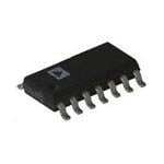
ICGOO电子元器件商城为您提供AD8040ARZ由Analog设计生产,在icgoo商城现货销售,并且可以通过原厂、代理商等渠道进行代购。 AD8040ARZ价格参考¥18.52-¥20.15。AnalogAD8040ARZ封装/规格:线性 - 放大器 - 仪表,运算放大器,缓冲器放大器, 通用 放大器 4 电路 满摆幅 14-SOIC。您可以下载AD8040ARZ参考资料、Datasheet数据手册功能说明书,资料中有AD8040ARZ 详细功能的应用电路图电压和使用方法及教程。
| 参数 | 数值 |
| -3db带宽 | 125MHz |
| 产品目录 | 集成电路 (IC)半导体 |
| 描述 | IC OPAMP GP 125MHZ RRO 14SOIC高速运算放大器 Quad Low-Pwr RRIO |
| DevelopmentKit | AD8040AR-EBZ |
| 产品分类 | Linear - Amplifiers - Instrumentation, OP Amps, Buffer Amps集成电路 - IC |
| 品牌 | Analog Devices |
| 产品手册 | |
| 产品图片 |
|
| rohs | 符合RoHS无铅 / 符合限制有害物质指令(RoHS)规范要求 |
| 产品系列 | 放大器 IC,高速运算放大器,Analog Devices AD8040ARZ- |
| 数据手册 | |
| 产品型号 | AD8040ARZ |
| 产品 | Voltage Feedback Amplifier |
| 产品培训模块 | http://www.digikey.cn/PTM/IndividualPTM.page?site=cn&lang=zhs&ptm=30008http://www.digikey.cn/PTM/IndividualPTM.page?site=cn&lang=zhs&ptm=26202 |
| 产品目录页面 | |
| 产品种类 | |
| 供应商器件封装 | 14-SOIC |
| 共模抑制比—最小值 | 90 dB |
| 关闭 | No Shutdown |
| 包装 | 管件 |
| 压摆率 | 63 V/µs |
| 商标 | Analog Devices |
| 增益带宽生成 | 40 MHz |
| 增益带宽积 | - |
| 安装类型 | 表面贴装 |
| 安装风格 | SMD/SMT |
| 封装 | Tube |
| 封装/外壳 | 14-SOIC(0.154",3.90mm 宽) |
| 封装/箱体 | SOIC-14 |
| 工作温度 | -40°C ~ 125°C |
| 工作电源电压 | 2.7 V to 12 V |
| 工厂包装数量 | 56 |
| 带宽 | 125 MHz |
| 拓扑结构 | Voltage Feedback |
| 放大器类型 | 通用 |
| 最大工作温度 | + 125 C |
| 最小工作温度 | - 40 C |
| 标准包装 | 56 |
| 电压-电源,单/双 (±) | 2.7 V ~ 12 V, ±1.35 V ~ 6 V |
| 电压-输入失调 | 2mV |
| 电压增益dB | 74 dB |
| 电流-电源 | 1.4mA |
| 电流-输入偏置 | 1.7µA |
| 电流-输出/通道 | 170mA |
| 电源电压-最大 | 12 V |
| 电源电压-最小 | 2.7 V |
| 电源电流 | 6 mA |
| 电路数 | 4 |
| 稳定时间 | 80 ns |
| 系列 | AD8040 |
| 视频文件 | http://www.digikey.cn/classic/video.aspx?PlayerID=1364138032001&width=640&height=505&videoID=2245193153001http://www.digikey.cn/classic/video.aspx?PlayerID=1364138032001&width=640&height=505&videoID=2245193159001 |
| 转换速度 | 60 V/us |
| 输入补偿电压 | 1.6 mV |
| 输出电流 | 5 mA |
| 输出类型 | 满摆幅 |
| 通道数量 | 4 Channel |


- 商务部:美国ITC正式对集成电路等产品启动337调查
- 曝三星4nm工艺存在良率问题 高通将骁龙8 Gen1或转产台积电
- 太阳诱电将投资9.5亿元在常州建新厂生产MLCC 预计2023年完工
- 英特尔发布欧洲新工厂建设计划 深化IDM 2.0 战略
- 台积电先进制程称霸业界 有大客户加持明年业绩稳了
- 达到5530亿美元!SIA预计今年全球半导体销售额将创下新高
- 英特尔拟将自动驾驶子公司Mobileye上市 估值或超500亿美元
- 三星加码芯片和SET,合并消费电子和移动部门,撤换高东真等 CEO
- 三星电子宣布重大人事变动 还合并消费电子和移动部门
- 海关总署:前11个月进口集成电路产品价值2.52万亿元 增长14.8%


PDF Datasheet 数据手册内容提取
Low Power, High Speed Rail-to-Rail Input/Output Amplifier Data Sheet AD8029/AD8030/AD8040 FEATURES CONNECTION DIAGRAMS Qualified for automotive applications Low power: 1.3 mA supply current/amplifier NC 1 8 DISABLE VOUT 1 6 +VS –IN 2 7 +VS High speed 1682005 Vn Ms/µ sHse zstt,l el–iwn3g dr atBit meb aen tdow 0i.d1%th (G = +1) –+VINS N34C = NO CONNECT65 VNOCUT 03679-A-004 –+VINS 23 + – 54 D–IINSABLE 03679-A-002 Rail-to-rail input and output Figure 1. SOIC-8 (R) Figure 2. SC70-6 (KS) No phase reversal, inputs 200 mV beyond rails Wide supply range: 2.7 V to 12 V Offset voltage: 6 mV maximum VOUT 1 1 14 VOUT 4 Low input bias current –IN 1 2 13 –IN 4 +0.7 µA to –1.5 µA +IN 1 3 12 +IN 4 Small packaging VOUT 1 1 8 +VS +VS 4 11 –VS SOIC-8, SC70-6, SOT23-8, SOIC-14, TSSOP-14 –IN 1 2 7 +VOUT 2 +IN 2 5 10 +IN 3 AAuPtPomLIoCtAivTe IsOafNetSy and vision systems +I–NV 1S 34 65 –+IINN 22 03679-A-003 VO–UINT 22 67 98 –VIONU 3T 3 03679-A-001 Battery-powered instrumentation Figure 3. SOIC-8 (R) and Figure 4. SOIC-14 (R) and Filters SOT23-8 (RJ) TSSOP-14 (RU) A-to-D drivers Buffering GENERAL DESCRIPTION The AD8029 (single), AD8030 (dual), and AD8040 (quad) are systems where component density requires lower power rail-to-rail input and output high speed amplifiers with a quiescent dissipation. The AD8040W is an automotive grade version, current of only 1.3 mA per amplifier. Despite their low power qualified for automotive applications. consumption, the amplifiers provide excellent performance with The AD8029/AD8030 are the only low power, rail-to-rail input 125 MHz small signal bandwidth and 60 V/µs slew rate. Analog and output high speed amplifiers available in SOT23 and SC70 Devices, Inc., proprietary XFCB process enables high speed and micro packages. The amplifiers are rated over the extended high performance on low power. industrial temperature range, –40°C to +125°C. This family of amplifiers exhibits true single-supply operation 5.0 with rail-to-rail input and output performance for supply voltages INPUT 4.5 ranging from 2.7 V to 12 V. The input voltage range extends OUTPUT 4.0 200 mV beyond each rail without phase reversal. The dynamic range of the output extends to within 40 mV of each rail. 3.5 V) 3.0 The AD8029/AD8030/AD8040 provide excellent signal quality E ( G with minimal power dissipation. At G = +1, SFDR is –72 dBc at A 2.5 T L 1 MHz and settling time to 0.1% is only 80 ns. Low distortion O 2.0 V and fast settling performance make these amplifiers suitable 1.5 drivers for single-supply analog-to-digital converters. 1.0 G = +1 The versatility of the AD8029/AD8030/AD8040 allows the user 0.5 VS = +5V to operate the amplifiers on a wide range of supplies while con- RL = 1kΩ TIED TO MIDSUPPLY 1µs/DIV 0 suming less than 6.5 mW of power. These features extend the TIME (µs) 03679-A-010 operation time in applications ranging from battery-powered Figure 5. Rail-to-Rail Response systems with large bandwidth requirements to high speed Rev. B Document Feedback Information furnished by Analog Devices is believed to be accurate and reliable. However, no responsibility is assumed by Analog Devices for its use, nor for any infringements of patents or other One Technology Way, P.O. Box 9106, Norwood, MA 02062-9106, U.S.A. rights of third parties that may result from its use. Specifications subject to change without notice. No license is granted by implication or otherwise under any patent or patent rights of Analog Devices. Tel: 781.329.4700 ©2003–2012 Analog Devices, Inc. All rights reserved. Trademarks and registered trademarks are the property of their respective owners. Technical Support www.analog.com
AD8029/AD8030/AD8040 Data Sheet TABLE OF CONTENTS Features .............................................................................................. 1 Theory of Operation ...................................................................... 16 Applications ....................................................................................... 1 Input Stage ................................................................................... 16 Connection Diagrams ...................................................................... 1 Output Stage ................................................................................ 16 General Description ......................................................................... 1 Applications ..................................................................................... 17 Specifications ..................................................................................... 3 Wideband Operation ................................................................. 17 Specifications with ±5 V Supply ................................................. 3 Output Loading Sensitivity ....................................................... 17 Specifications with +5 V Supply ................................................. 4 Disable Pin .................................................................................. 18 Specifications with +3 V Supply ................................................. 5 Circuit Considerations .............................................................. 19 Absolute Maximum Ratings ............................................................ 7 Design Tools and Technical Support ....................................... 19 Maximum Power Dissipation ..................................................... 7 Outline Dimensions ....................................................................... 20 ESD Caution .................................................................................. 7 Ordering Guide .......................................................................... 21 Typical Performance Characteristics ............................................. 8 REVISION HISTORY 10/12—Rev. A to Rev. B Added Automotive Model, AD8040W ............................ Universal Changes to Features Section............................................................ 1 Changes to General Description Section ...................................... 1 Changes to Specifications Section, Table 1, Added Automotive Specifications ..................................................................................... 3 Moved ESD Caution to Absolute Maximum Ratings Section .... 7 Changes to Figure 17 ........................................................................ 9 Updated Outline Dimensions ....................................................... 20 Changes to Ordering Guide .......................................................... 21 11/03—Rev. 0 to Rev. A Added AD8040 part ....................................................... Universal Change to Figure 5 ....................................................................... 1 Changes to Specifications ............................................................ 3 Changes to Figures 10–12 ............................................................ 7 Change to Figure 14 ..................................................................... 8 Changes to Figures 20 and 21 ..................................................... 9 Inserted new Figure 36 ............................................................... 11 Change to Figure 40 ................................................................... 12 Inserted new Figure 41 ............................................................... 12 Added Output Loading Sensitivity section ............................. 16 Changes to Table 5 ...................................................................... 17 Changes to Power Supply Bypassing section .......................... 18 Changes to Ordering Guide ...................................................... 20 Rev. B | Page 2 of 24
Data Sheet AD8029/AD8030/AD8040 SPECIFICATIONS SPECIFICATIONS WITH ±5 V SUPPLY Table 1. V = ±5 V @ T = 25°C, G = +1, R = 1 kΩ to ground, unless otherwise noted. All specifications are per amplifier. S A L Parameter Conditions Min Typ Max Unit DYNAMIC PERFORMANCE –3 dB Bandwidth G = +1, VO = 0.1 V p-p 80 125 MHz AD8040W only: TMIN to TMAX 80 MHz G = +1, VO = 2 V p-p 14 19 MHz AD8040W only: TMIN to TMAX 9 MHz Bandwidth for 0.1 dB Flatness G = +2, VO = 0.1 V p-p 6 MHz Slew Rate G = +1, VO = 2 V Step 62 V/μs G = –1, VO = 2 V Step 63 V/μs Settling Time to 0.1% G = +2, VO = 2 V Step 80 ns NOISE/DISTORTION PERFORMANCE Spurious Free Dynamic Range (SFDR) fC = 1 MHz, VO = 2 V p-p –74 dBc fC = 5 MHz, VO = 2 V p-p –56 dBc Input Voltage Noise f = 100 kHz 16.5 nV/√Hz Input Current Noise f = 100 kHz 1.1 pA/√Hz Crosstalk (AD8030/AD8040) f = 5 MHz, VIN = 2 V p-p –79 dB DC PERFORMANCE Input Offset Voltage PNP Active, VCM = 0 V 1.6 5 mV AD8040W only: TMIN to TMAX 9.5 mV NPN Active, VCM = 4.5 V 2 6 mV AD8040W only: TMIN to TMAX 9.5 mV Input Offset Voltage Drift TMIN to TMAX 30 μV/°C Input Bias Current1 NPN Active, VCM = 4.5 V 0.7 1.3 μA TMIN to TMAX 1 μA AD8040W only: TMIN to TMAX 1.3 μA PNP Active, VCM = 0 V –1.7 –2.8 μA TMIN to TMAX 2 μA AD8040W only: TMIN to TMAX –2.8 μA Input Offset Current ±0.1 ±0.9 μA AD8040W only: TMIN to TMAX ±0.9 μA Open-Loop Gain Vo = ±4.0 V 65 74 dB AD8040W only: TMIN to TMAX 62 dB INPUT CHARACTERISTICS Input Resistance 6 MΩ Input Capacitance 2 pF Input Common-Mode Voltage Range –5.2 to +5.2 V Common-Mode Rejection Ratio VCM = –4.5 V to +3 V, RL = 10 kΩ 80 90 dB AD8040W only: TMIN to TMAX 80 dB DISABLE PIN (AD8029) DISABLE Low Voltage –VS + 0.8 V DISABLE Low Current –6.5 μA DISABLE High Voltage –VS + 1.2 V DISABLE High Current 0.2 μA Turn-Off Time 50% of DISABLE to <10% of Final VO, 150 ns VIN = –1 V, G = –1 Turn-On Time 50% of DISABLE to <10% of Final VO, 85 ns VIN = –1 V, G = –1 OUTPUT CHARACTERISTICS Output Overdrive Recovery Time (Rising/Falling Edge) VIN = +6 V to –6 V, G = –1 55/45 ns Output Voltage Swing RL = 1 kΩ –VS + 0.22 +VS – 0.22 V AD8040W only: TMIN to TMAX –VS + 0.22 +VS – 0.22 V RL = 10 kΩ –VS + 0.05 +VS – 0.05 V AD8040W only: TMIN to TMAX –VS + 0.05 +VS – 0.05 V Rev. B | Page 3 of 24
AD8029/AD8030/AD8040 Data Sheet Parameter Conditions Min Typ Max Unit Short-Circuit Current Sinking and Sourcing 170/160 mA Off Isolation (AD8029) VIN = 0.1 V p-p, f = 1 MHz, DISABLE = Low –55 dB Capacitive Load Drive 30% Overshoot 20 pF POWER SUPPLY Operating Range 2.7 12 V Quiescent Current/Amplifier 1.4 1.5 mA AD8040W only: TMIN to TMAX 1.85 mA Quiescent Current (Disabled) DISABLE = Low, AD8029 only 150 200 µA Power Supply Rejection Ratio Vs ± 1 V 73 80 dB AD8040W only: TMIN to TMAX 72 dB 1 Plus, +, (or no sign) indicates current into pin; minus (–) indicates current out of pin. SPECIFICATIONS WITH +5 V SUPPLY Table 2. V = 5 V @ T = 25°C, G = +1, R = 1 kΩ to midsupply, unless otherwise noted. All specifications are per amplifier. S A L Parameter Conditions Min Typ Max Unit DYNAMIC PERFORMANCE –3 dB Bandwidth G = +1, V = 0.1 V p-p 80 120 MHz O AD8040W only: TMIN to TMAX 80 MHz G = +1, V = 2 V p-p 13 18 MHz O AD8040W only: TMIN to TMAX 8 MHz Bandwidth for 0.1 dB Flatness G = +2, V = 0.1 V p-p 6 MHz O Slew Rate G = +1, V = 2 V Step 55 V/µs O G = –1, V = 2 V Step 60 V/µs O Settling Time to 0.1% G = +2, V = 2 V Step 82 ns O NOISE/DISTORTION PERFORMANCE Spurious Free Dynamic Range (SFDR) f = 1 MHz, V = 2 V p-p –73 dBc C O f = 5 MHz, V = 2 V p-p –55 dBc C O Input Voltage Noise f = 100 kHz 16.5 nV/√Hz Input Current Noise f = 100 kHz 1.1 pA/√Hz Crosstalk (AD8030/AD8040) f = 5 MHz, V = 2 V p-p –79 dB IN DC PERFORMANCE Input Offset Voltage PNP Active, V = 2.5 V 1.4 5 mV CM AD8040W only: TMIN to TMAX 8.5 mV NPN Active, V = 4.5 V 1.8 6 mV CM AD8040W only: TMIN to TMAX 8.5 mV Input Offset Voltage Drift T to T 25 µV/°C MIN MAX Input Bias Current1 NPN Active, V = 4.5 V 0.8 1.2 µA CM T to T 1 µA MIN MAX PNP Active, V = 2.5 V –1.8 –2.8 µA CM T to T 2 µA MIN MAX Input Offset Current ±0.1 ±0.9 µA AD8040W only: TMIN to TMAX ±0.9 µA Open-Loop Gain V = 1 V to 4 V 65 74 dB o AD8040W only: TMIN to TMAX 62 dB INPUT CHARACTERISTICS Input Resistance 6 MΩ Input Capacitance 2 pF Input Common-Mode Voltage Range –0.2 to +5.2 V Common-Mode Rejection Ratio V = 0.25 V to 2 V, R = 10 kΩ 80 90 dB CM L AD8040W only: TMIN to TMAX 80 dB DISABLE PIN (AD8029) DISABLE Low Voltage –VS + 0.8 V DISABLE Low Current –6.5 µA DISABLE High Voltage –VS + 1.2 V Rev. B | Page 4 of 24
Data Sheet AD8029/AD8030/AD8040 Parameter Conditions Min Typ Max Unit DISABLE High Current 0.2 µA Turn-Off Time 50% of DISABLE to <10% of Final VO, 155 ns V = –1 V, G = –1 IN Turn-On Time 50% of DISABLE to <10% of Final VO, 90 ns V = –1 V, G = –1 IN OUTPUT CHARACTERISTICS Overdrive Recovery Time (Rising/Falling Edge) V = –1 V to +6 V, G = –1 45/50 ns IN Output Voltage Swing R = 1 kΩ –V + 0.17 +V – 0.17 V L S S AD8040W only: TMIN to TMAX –VS + 0.17 +VS – 0.17 V R = 10 kΩ –V + 0.04 +V – 0.04 V L S S AD8040W only: TMIN to TMAX –VS + 0.04 +VS – 0.04 V Short-Circuit Current Sinking and Sourcing 95/60 mA Off Isolation (AD8029) V = 0.1 V p-p, f = 1 MHz, DISABLE = Low –55 dB in Capacitive Load Drive 30% Overshoot 15 pF POWER SUPPLY Operating Range 2.7 12 V Quiescent Current/Amplifier 1.3 1.5 mA AD8040W only: TMIN to TMAX 1.75 mA Quiescent Current (Disabled) DISABLE = Low, AD8029 only 140 200 µA Power Supply Rejection Ratio V ± 1 V 73 80 dB S AD8040W only: TMIN to TMAX 72 dB 1 Plus, +, (or no sign) indicates current into pin; minus (–) indicates current out of pin. SPECIFICATIONS WITH +3 V SUPPLY Table 3. V = +3 V @ T = 25°C, G = +1, R = 1 kΩ to midsupply, unless otherwise noted. All specifications are per amplifier. S A L Parameter Conditions Min Typ Max Unit DYNAMIC PERFORMANCE –3 dB Bandwidth G = +1, V = 0.1 V p-p 80 112 MHz O AD8040W only: TMIN to TMAX 80 MHz G = +1, V = 2 V p-p 13 18 MHz O AD8040W only: TMIN to TMAX 8 MHz Bandwidth for 0.1 dB Flatness G = +2, V = 0.1 V p-p 6 MHz O Slew Rate G = +1, V = 2 V Step 55 V/µs O G = –1, V = 2 V Step 57 V/µs O Settling Time to 0.1% G = +2, V = 2 V Step 110 ns O NOISE/DISTORTION PERFORMANCE Spurious Free Dynamic Range (SFDR) f = 1 MHz, V = 2 V p-p –72 dBc C O f = 5 MHz, V = 2 V p-p –60 dBc C O Input Voltage Noise f = 100 kHz 16.5 nV/√Hz Input Current Noise f = 100 kHz 1.1 pA/√Hz Crosstalk (AD8030/AD8040) f = 5 MHz, V = 2 V p-p –80 dB IN DC PERFORMANCE Input Offset Voltage PNP Active, V = 1.5 V 1.1 5 mV CM AD8040W only: TMIN to TMAX 8 mV NPN Active, V = 2.5 V 1.6 6 mV CM AD8040W only: TMIN to TMAX 8 mV Input Offset Voltage Drift T to T 24 µV/°C MIN MAX Input Bias Current1 NPN Active, V = 2.5 V 0.7 1.2 µA CM T to T 1 µA MIN MAX Input Bias Current1 PNP Active, V = 1.5 V –1.5 –2.5 µA CM T to T 1.6 µA MIN MAX Input Offset Current ±0.1 ±0.9 µA AD8040W only: TMIN to TMAX ±0.9 µA Rev. B | Page 5 of 24
AD8029/AD8030/AD8040 Data Sheet Parameter Conditions Min Typ Max Unit Open-Loop Gain V = 0.5 V to 2.5 V 64 73 dB o AD8040W only: TMIN to TMAX 62 dB INPUT CHARACTERISTICS Input Resistance 6 MΩ Input Capacitance 2 pF Input Common-Mode Voltage Range –0.2 to +3.2 V Common-Mode Rejection Ratio V = 0.25 V to 1.25 V, R = 10 kΩ 78 88 dB CM L AD8040W only: TMIN to TMAX 78 dB DISABLE PIN (AD8029) DISABLE Low Voltage –VS + 0.8 V DISABLE Low Current –6.5 µA DISABLE High Voltage –VS + 1.2 V DISABLE High Current 0.2 µA Turn-Off Time 50% of DISABLE to <10% of Final VO, 165 ns V = –1 V, G = –1 IN Turn-On Time 50% of DISABLE to <10% of Final VO, 95 ns V = –1 V, G = –1 IN OUTPUT CHARACTERISTICS Output Overdrive Recovery Time (Rising/Falling Edge) V = –1 V to +4 V, G = –1 75/100 ns IN Output Voltage Swing R = 1 kΩ –V + 0.09 +V – 0.09 V L S S AD8040W only: TMIN to TMAX –VS + 0.09 +VS – 0.09 V R = 10 kΩ –V + 0.04 +V – 0.04 V L S S AD8040W only: TMIN to TMAX –VS + 0.04 +VS – 0.04 V Short-Circuit Current Sinking and Sourcing 80/40 mA Off Isolation (AD8029) V = 0.1 V p-p, f = 1 MHz, DISABLE = Low –55 dB IN Capacitive Load Drive 30% Overshoot 10 pF POWER SUPPLY Operating Range 2.7 12 V Quiescent Current/Amplifier 1.3 1.4 mA AD8040W only: TMIN to TMAX 1.75 mA Quiescent Current (Disabled) DISABLE = Low, AD8029 only 145 200 µA Power Supply Rejection Ratio V ± 1 V 70 76 dB S AD8040W only: TMIN to TMAX 68 dB 1 Plus, +, (or no sign) indicates current into pin; minus (–) indicates current out of pin. Rev. B | Page 6 of 24
Data Sheet AD8029/AD8030/AD8040 ABSOLUTE MAXIMUM RATINGS RMS output voltages should be considered. If R is referenced to Table 4. AD8029/AD8030/AD8040 Stress Ratings L V–, as in single-supply operation, then the total drive power is Parameter Rating S V × I . Supply Voltage 12.6 V S OUT Power Dissipation See Figure 6 If the rms signal levels are indeterminate, consider the worst Common-Mode Input Voltage ±VS ± 0.5 V case, when VOUT = VS/4 for RL to midsupply: DStioffreargeen tTieaml Inppeuratt Vuorelt age –±615.8° CV to +125°C PD =(VS×IS)+(VS/4)2 R Operating Temperature Range –40°C to +125°C L Lead Temperature Range 300°C In single-supply operation with RL referenced to VS–, worst case (Soldering 10 sec) is V = V/2. OUT S Junction Temperature 150°C Airflow increases heat dissipation, effectively reducing θ . Also, JA Stresses above those listed under Absolute Maximum Ratings more metal directly in contact with the package leads from may cause permanent damage to the device. This is a stress metal traces, through holes, ground, and power planes reduce rating only; functional operation of the device at these or any the θJA. Care must be taken to minimize parasitic capacitances other conditions above those indicated in the operational at the input leads of high speed op amps, as discussed in the section of this specification is not implied. Exposure to absolute PCB Layout section. maximum rating conditions for extended periods may affect Figure 6 shows the maximum safe power dissipation in the device reliability. package versus the ambient temperature for the SOIC-8 MAXIMUM POWER DISSIPATION (125°C/W), SOT23-8 (160°C/W), SOIC-14 (90°C/W), TSSOP-14 (120°C/W), and SC70-6 (208°C/W) packages on a The maximum safe power dissipation in the AD8029/AD8030/ JEDEC standard 4-layer board. θ values are approximations. AD8040 package is limited by the associated rise in junction JA temperature (T) on the die. The plastic encapsulating the die 2.5 J locally reaches the junction temperature. At approximately 150°C, which is the glass transition temperature, the plastic W) N (2.0 changes its properties. Even temporarily exceeding this TIO SOIC-14 temperature limit may change the stresses that the package PA SI1.5 exerts on the die, permanently shifting the parametric DIS TSSOP-14 performance of the AD8029/AD8030/AD8040. Exceeding a ER SOIC-8 W junction temperature of 175°C for an extended period can PO1.0 SOT-23-8 result in changes in silicon devices, potentially causing failure. M U M The still-air thermal properties of the package and PCB (θJA), AXI0.5 SC70-6 M ambient temperature (T ), and the total power dissipated in the A Tpahcek jaugnec (tPioDn) dteemteprmeriantue rteh ec ajnu nbcet icoanlc tuelmatpeedr aastu re of the die. 0–40–30–20–10 0A1M0BI2E0NT3 0TE4M0PE5R0A6T0UR7E0 (°8C0) 90100110120 03679-A-018 TJ = TA + (PD × θJA) Figure 6. Maximum Power Dissipation The power dissipated in the package (PD) is the sum of the Output Short Circuit quiescent power dissipation and the power dissipated in the Shorting the output to ground or drawing excessive current package due to the load drive for all outputs. The quiescent from the AD8029/AD8030/AD8040 could cause catastrophic power is the voltage between the supply pins (V) times the S failure. quiescent current (I). Assuming the load (R) is referenced to S L ESD CAUTION midsupply, the total drive power is V/2 × I , some of which is S OUT dissipated in the package and some in the load (V × I ). OUT OUT The difference between the total drive power and the load power is the drive power dissipated in the package. P = Quiescent Power + (Total Drive Power – Load Power) D PD =(VS×IS)+V2S ×VORULT –VORULT2 Rev. B | Page 7 of 24
AD8029/AD8030/AD8040 Data Sheet TYPICAL PERFORMANCE CHARACTERISTICS Default Conditions: V = 5 V (T = 25°C, R = 1 kΩ tied to midsupply, unless otherwise noted.) S A L 01 G =–1 0.2 DASHED LINES: VOUT = 2V p-p RF = 1kΩ B) –1 RF = RG = 1kΩ B) 0.1 SOLID LINES: VOUT = 0.1V p-p d d GAIN ( ––32 RF = 9kΩ, RGG == 1+k1Ω0 GAIN (–0.10 P –4 P G = +1 O O O –5 O–0.2 ED-L –6 RF = RGG = =1 k+Ω2 GRF = = + 01Ω ED-L–0.3 S –7 S O O CL –8 CL–0.4 D –9 D G = +2 LIZE–10 LIZE–0.5 MA–11 MA–0.6 OR–12 OR N N–0.7 –13 VO = 0.1V p-p –14 –0.8 0.1 1 10 100 1000 1 10 100 FREQUENCY (MHz) 03679-0-004 FREQUENCY (MHz) 03679-A-011 Figure 7. Small Signal Frequency Response for Various Gains Figure 10. 0.1 dB Flatness Frequency Response 1 1 G = +1 +3V G = +2 0 VO = 0.1V p-p 0 VO = 0.1V p-p B) RF = 1kΩ –1 ±5V N (d –1 B) GAI N (d –2 OP –2 AI O D-LOOP G ––43 +5V CLOSED-L ––43 ±5V CLOSE ––65 ALIZED ––65 M +5V R –7 NO –7 +3V –8 –8 1 10 100 1000 1 10 100 FREQUENCY (MHz) 03679-0-005 FREQUENCY (MHz) 03679-A-012 Figure 8. Small Signal Frequency Response for Various Supplies Figure 11. Small Signal Frequency Response for Various Supplies 1 1 G = +1 G = +2 RF = 1kΩ 0 VO = 2V p-p 0 VO = 2V p-p ±5V dB) –1 N ( –1 B) GAI VS =±5 AIN (d –2 +3V OOP –2 VS = +5 CLOSED-LOOP G ––––6543 ALIZED CLOSED-L ––––6543 VS = +3 M +5V R –7 NO –7 –8 –8 1 10 100 1 10 100 FREQUENCY (MHz) 03679-0-006 FREQUENCY (MHz) 03679-A-013 Figure 9. Large Signal Frequency Response for Various Supplies Figure 12. Large Signal Frequency Response for Various Supplies Rev. B | Page 8 of 24
Data Sheet AD8029/AD8030/AD8040 6 2 5 GVO = = + 01.1V p-p 20pF 1 GVO = = + 01.1V p-p VICM = VS+– 0.2V 34 10pF 0 VICM = 0V B) 2 B)–1 GAIN (d 01 5pF GAIN (d–2 VICM = VS– + 0.2V ED-LOOP –––321 0pF ED-LOOP ––43 OS –4 OS–5 CL –5 CL–6 –6 –7 –7 –8 –8 1 10 100 1000 1 10 100 1000 FREQUENCY (MHz) 03679-0-010 FREQUENCY (MHz) 03679-0-013 Figure 13. Small Signal Frequency Response for Various CLOAD Figure 16. Small Signal Frequency Response for Various Input Common-Mode Voltages 1 2 G = +2 G = +1 +125°C B) 0 RF = 1kΩ 1 VO = 0.1V p-p +85°C OP GAIN (d ––21 N (dB) –10 –40°C +25°C O AI OSED-L ––43 OOP G –2 CL D-L –3 ZED –5 2V p-p OSE ALI –6 1V p-p CL –4 M R 0.1V p-p NO –7 –5 –8 –6 1 10 100 1 10 100 1000 FREQUENCY (MHz) 03679-A-014 FREQUENCY (MHz) 03679-0-014 Figure 14. Frequency Response for Various Output Amplitudes Figure 17. Small Signal Frequency Response vs. Temperature 80 225 1 G = +1 70 0 VO = 2V p-p +125°C 60 180 s) –1 e AIN (dB) 5400 135 E (Degre AIN (dB) –2 +25+°C85°C OP G 30 PHAS OP G –3 N-LO 20 90 OOP D-LO –4 –40°C OPE 100 45 OPEN-L CLOSE ––65 –10 –7 –20 0 –8 10 100 1k 10k 100k 1M 10M 100M 1G 1 10 100 FREQUENCY (Hz) 03679-0-054 FREQUENCY (MHz) 03679-0-015 Figure 15. Open-Loop Gain and Phase vs. Frequency Figure 18. Large Signal Frequency Response vs. Temperature Rev. B | Page 9 of 24
AD8029/AD8030/AD8040 Data Sheet –35 –40 G = +1 G = +1 VOUT = 2V p-p VOUT = 2V p-p –45 RL = 1kΩ –50 SECOND HARMONIC: SOLID LINE SECOND HARMONIC: SOLID LINE THIRD HARMONIC: DASHED LINE N (dBc) –55 THIRD HARMONIC: DASHED LINE N (dBc) –60 O O STORTI –65 VS = +3V STORTI –70 RL = 1kΩ DI –75 DI –80 C C NI NI MO –85 MO –90 HAR VS = +5V VS =±5V HAR RL = 5kΩ –95 –100 RL = 2kΩ –105 –110 0.01 0.1 1 10 0.01 0.1 1 10 FREQUENCY (MHz) 03679-0-016 FREQUENCY (MHz) 03679-0-075 Figure 19. Harmonic Distortion vs. Frequency and Supply Voltage Figure 22. Harmonic Distortion vs. Frequency and Load –40 –40 G = +2 G = +1 –45 FRRF E=Q 1 k=Ω 1MHz VFROUETQ = = 2 1VM pH-pz –50 RTION (dBc)––5550 VS = +3V VS = +5V VS = +10V TION (dBc) –60 VS = +3V VS = +5V O R ST–60 TO –70 ONIC DI–65 NIC DIS –80 M O AR–70 RM H A H –90 –75 SECOND HARMONIC: SOLID LINE SECOND HARMONIC: SOLID LINE THIRD HARMONIC: DASHED LINE THIRD HARMONIC: DASHED LINE –80 –100 0.5 1.5 2.5 3.5 4.5 5.5 6.5 7.5 8.5 9.5 1.0 1.5 2.0 2.5 3.0 3.5 4.0 OUTPUT AMPLITUDE (V p-p) 03679-A-015 INPUT COMMON-MODE VOLTAGE (V) 03679-0-020 Figure 20. Harmonic Distortion vs. Output Amplitude Figure 23. Harmonic Distortion vs. Input Common Mode Voltage –30 1000 100 VS = +5V VOUT = 2.0V p-p –40 RL = 1kΩ RF = 1kΩ c) –50 RTION (dB –60 G =–1G = +2 E (nV/ Hz)100 10 E (pA/ Hz) C DISTO ––8700 GE NOIS VOLTAGE NOISE NT NOIS RMONI –90 VOLTA 10 CURRENT NOISE 1 CURRE A H G = +1 –100 SECOND HARMONIC: SOLID LINE THIRD HARMONIC: DASHED LINE –110 1 0.1 0.01 0.1 1 10 10 100 1k 10k 100k 1M 10M FREQUENCY (MHz) FREQUENCY (Hz) 03679-A-016 03679-0-069 Figure 21. Harmonic Distortion vs. Frequency and Gain Figure 24. Voltage and Current Noise vs. Frequency Rev. B | Page 10 of 24
Data Sheet AD8029/AD8030/AD8040 100 100 75 GVS = = +±12.5V 75 GVS = = +±12.5V CCLL == 1200ppFF CL = 5pF V) 50 V) 50 m m E ( 25 E ( 25 G G A A T T OL 0 OL 0 V V T T PU–25 PU–25 T T U U O O –50 –50 –75 –75 25mV/DIV 20ns/DIV 25mV/DIV 20ns/DIV –100 –100 TIME (ns) 03679-0-022 TIME (ns) 03679-0-025 Figure 25. Small Signal Transient Response Figure 28. Small Signal Transient Response with Capacitive Load 2.5 G = +1 5.0 4V p-p 2.0 VS =±2.5V 4.5 INPUT 1.5 4.0 PUT VOLTAGE (V) –100...0505 2V p-p VOLTAGE (V) 2233....0505 T U –1.0 O 1.5 –1.5 1.0 G = +1 OUTPUT –2.0 0.5 VS = +5V –2.5 0.5V/DIV TIME (ns) 25ns/DIV 03679-A-023 0 RL = 1kΩ TIED TO MIDSTUIMPEP L(SYeconds) 0316µ79s-/0D-0IV59 Figure 26. Large Signal Transient Response Figure 29. Rail-to-Rail Response, G = +1 4 4 INPUT G =–1 (RF = 1kΩ) INPUT G = +1 3 RVSL == ±12k.Ω5V 3 RVSL == ±12k.Ω5V 2 2 OUTPUT VOLTAGE (V)–110 OUTPUT OUTPUT VOLTAGE (V)–110 OUTPUT –2 –2 –3 –3 1V/DIV 200ns/DIV 1V/DIV 200ns/DIV –4 –4 TIME (ns) 03679-0-024 TIME (ns) 03679-0-027 Figure 27. Output Overdrive Recovery Figure 30. Input Overdrive Recovery Rev. B | Page 11 of 24
AD8029/AD8030/AD8040 Data Sheet G = +2 VIN (250mV/DIV) G = +2 VS =±2.5V VOUT (500mV/DIV) +1V +0.1% +0.1% VOUT– 2VIN (0.1%/DIV) VOUT– 2VIN (0.1%/DIV) –0.1% –0.1% VOUT (500mV/DIV) –1V 500ns/DIV 20ns/DIV 03679-0-062 03679-0-063 Figure 31. Long-Term Settling Time Figure 34.0.1% Short-Term Settling Time –20 0 –10 –30 –20 –40 +PSRR –30 –50 B) dB)–40 R (d–60 RR (–50 R S CM–70 P–60 –70 –80 –PSRR –80 –90 –90 –100 –100 1k 10k 100k 1M 10M 100M 1G 1k 10k 100k 1M 10M 100M 1G FREQUENCY (Hz) FREQUENCY (Hz) 03679-0-078 03679-0-033 Figure 32. Common-Mode Rejection Ratio vs. Frequency Figure 35. PSRR vs. Frequency –20 –30 G = +1 VIN –30 RDLIS =A 1BkLΩE = LOW –40 50Ω DRIVE A1MkΩP VIN = 0.1V p-p –50 –60 LISTEN AMP OUTPUT (dB) ––5400 OSSTALK (dB) –––789000 CROSSTALK = 20log(VV1VOOkINUΩUTT) A(ADM8P0 320 DRIVE –60 CR–100 AMP 1 LISTEN) –110 –70 AD8040 –120 (AMP 4 DRIVE –800.1 1 FREQUE1N0CY (MHz) 100 03679-0-0150500 –1300.01 0.1 FR1E.0QAUMEPN 1C LYI S(MT1EH0Nz)) 100 1000 03679-A-005 Figure 33. AD8029 Off-Isolation vs. Frequency Figure 36. AD8030/AD8040 Crosstalk vs. Frequency Rev. B | Page 12 of 24
Data Sheet AD8029/AD8030/AD8040 2.5 4 RL = 1kΩTO 2.0 MIDSUPPLY 3 G = +1 VS = +3V VS = +5V VS = +10V µRRENT (A) 011...505 OLTAGE (mV) 12 VS = +3V VS = +5V VS = +10V U 0 V 0 S C ET A –0.5 S INPUT BI ––11..50 NPUT OFF––21 I –3 –2.0 –2.5 –4 –1 0 1 2 3 4 5 6 7 8 9 10 11 –1 0 1 2 3 4 5 6 7 8 9 10 11 INPUT COMMON-MODE VOLTAGE (V) INPUT COMMON-MODE VOLTAGE (V) 03679-0-074 03679-A-017 Figure 37. Input Bias Current vs. Input Common-Mode Voltage Figure 40. Input Offset Voltage vs. Input Common-Mode Voltage –1.0 1.0 4 A) A) 3 µ µ CTIVE) ( –1.2 NPN ACTIVE 0.8 CTIVE) ( E (mV) 2 VS = ±5V T (PNP A –1.4 VS =±5 VS = +5 VS = +3 0.6 T (NPN A VOLTAG 10 VS = +5V EN EN ET RR –1.6 0.4 RR FS –1 CU CU OF VS = +3V AS AS UT –2 T BI –1.8 PNP ACTIVE 0.2 T BI INP PU PU –3 N N I I –2.0–40 –25 –10 5 T2E0MPE3R5ATU5R0E (°6C5) 80 95 110 1250 –4–40 –25 –10 5 T2E0MPE3R5ATU5R0E (°6C5) 80 95 110 125 03679-A-006 03679-0-073 Figure 38. Input Bias Current vs. Temperature Figure 41. Input Offset Voltage vs. Temperature 1.8 120 COUNT = 1088 MEAN = 0.44mV 1.7 STDEV = 1.05mV 100 1.6 VS = +5V A) 1.5 T (m 1.4 VS =±5V Y 80 N C E N RR 1.3 UE 60 CU VS = +3V EQ Y 1.2 R PL F 40 P 1.1 U S 1.0 20 0.9 0.8 0 –40 –20 0 20 40 60 80 100 120 –5 –4 –3 –2 –1 0 1 2 3 4 5 TEMPERATURE (°C) INPUT OFFSET VOLTAGE (mV) 03679-0-067 03679-0-064 Figure 39 Quiescent Supply Current vs. Temperature Figure 42. Input Offset Voltage Distribution Rev. B | Page 13 of 24
AD8029/AD8030/AD8040 Data Sheet 1M 1000 DISABLE = LOW G = +1 100k Ω) Ω)100 E (10k E ( C C N N A A D D PE 1k PE 10 M M T I T I U U P100 P T T U U O O 1 10 1 0.1 100k 1M 10M 100M 1G 1k 10k 100k 1M 10M 100M 1G FREQUENCY (Hz) FREQUENCY (Hz) 03679-0-061 03679-0-060 Figure 43. AD8029 Output Impedance vs. Frequency, Disabled Figure 45. Output Impedance vs. Frequency, Enabled 0.5 2.0 0.4 LTOOA MDID RSEUSPISPTLAYNCE TIED 1.5 VS =±2.5V E (V) 0.3 V) 1.0 G m ATION VOLTA 00..012 VS = +3V VS = +5V VS =±5V VOL– VS R VOLTAGE ( 0.05 RL = 10kΩ ATUR–0.1 VOH– VS ERRO–0.5 RL = 1kΩ UT S–0.2 PUT –1.0 TP–0.3 IN U O –1.5 –0.4 –0.5 –2.0 100 1000 10000 –2.5 –2.0 –1.5 –1.0 –0.5 –0 0.5 1.0 1.5 2.0 2.5 LOAD RESISTANCE (Ω) OUTPUT VOLTAGE (V) 03679-0-041 03679-0-072 Figure 44. Output Saturation Voltage vs. Load Resistance Figure 46. Input Error Voltage vs. Output Voltage 170 V)150 VS =±5V m E ( AG130 T L O V110 N O TI RA 90 VS = +5V U T A S 70 T U P OUT 50 VS = +3V RSOL L=I D1k LΩIN TEIE: DV ST+O– M VIODHSUPPLY DASHED LINE: VOL– VS– 30 –40 –25 –10 5 20 35 50 65 80 95 110 125 TEMPERATURE (°C) 03679-0-066 Figure 42. Output Saturation Voltage vs. Temperature Rev. B | Page 14 of 24
Data Sheet AD8029/AD8030/AD8040 1.5 1 DISABLE (–0.5V TO–2V) VS = +3V, +5V, +10V 0 1.0 MPLITUDE (V) 0.05 RRLL == 110k0ΩΩ OUTPUT DISABLED µCURRENT (A) –––321 TPUT A–0.5 RL = 10kΩ LE PIN –4 U B O A S –5 DI –1.0 –6 VS =±2.5V G =–1 (RF = 1kΩ) –1.5 –7 0 50 100 150 200 250 300 350 0 0.8 1 1.2 2 3 TIME (ns) 03679-A-020 DISABLE PIN VOLTAGE (V) 03679-A-022 Figure 47. AD8029 DISABLE Turn-Off Timing Figure 49. AD8029 DISABLE Pin Current vs. DISABLE Pin Voltage 1.5 DISABLE (–2V TO–0.5V) 1.0 OUTPUT ENABLED V) E ( 0.5 D U T LI P 0 M A UTPUT –0.5 RRLL == 110k0ΩΩ O RL = 10kΩ –1.0 VS =±2.5V G =–1 (RF = 1kΩ) –1.5 0 50 100 150 200 250 300 350 TIME (ns) 03679-A-021 Figure 48. AD8029 DISABLE Turn-On Timing Rev. B | Page 15 of 24
AD8029/AD8030/AD8040 Data Sheet THEORY OF OPERATION +VS RTH SPD ITAIL DISABLE +VS–1.2V Q9 OUTPUT TO DISABLE ITH R1 R2 R3 R4 BUFFER CIRCUITRY –VS Q10 AD8029 ONLY Q1 MTOP CMT IN– Q5 Q6 Q2 VOUT CMB Q7 Q8 Q3 IN+ Q4 MBOT R5 R6 R7 R8 Q11 OUT IN COM –VS 03679-0-051 Figure 50. Simplified Schematic The AD8029 (single), AD8030 (dual), and AD8040 (quad) are OUTPUT STAGE rail-to-rail input and output amplifiers fabricated using Analog The currents derived from the PNP and NPN input differential Devices’ XFCB process. The XFCB process enables the pairs are injected into the current mirrors M and M , thus BOT TOP AD8029/ AD8030/AD8040 to operate on 2.7 V to 12 V supplies establishing a common-mode signal voltage at the input of the with a 120 MHz bandwidth and a 60 V/µs slew rate. A output buffer. simplified sche-matic of the AD8029/AD8030/AD8040 is The output buffer performs three functions: shown in Figure 50. INPUT STAGE 1. It buffers and applies the desired signal voltage to the output devices, Q and Q . 10 11 For input common-mode voltages less than a set threshold 2. It senses the common-mode current level in the output (1.2 V below V ), the resistor degenerated PNP differential CC devices. pair (comprising Q toQ) carries the entire I current, 1 4 TAIL allowing the input voltage to go 200 mV below –V. Conversely, 3. It regulates the output common-mode current by S input common-mode voltages exceeding the same threshold establishing a common-mode feedback loop. cause I to be routed away from the PNP differential pair and TAIL The output devices Q and Q work in a common-emitter 10 11 into the NPN differential pair through transistor Q. Under this 9 configuration, and are Miller-compensated by internal condition, the input common-mode voltage is allowed to rise capacitors, C and C . MT MB 200 mV above +V while still maintaining linear amplifier S The output voltage compliance is set by the output devices’ behavior. The transition between these two modes of operation collector resistance R (about 25 Ω), and by the required load leads to a sudden, temporary shift in input stage transconduc- C current I. For instance, a light equivalent load (5 kΩ) allows the tance, g , and dc parameters (such as the input offset voltage L m output voltage to swing to within 40 mV of either rail, while V ), which in turn adversely affect the distortion performance. OS heavier loads cause this figure to deteriorate as R × I. The SPD block shortens the duration of this transition, thus C L improving the distortion performance. As shown in Figure 50, the input differential pair is protected by a pair of two series diodes, connected in anti-parallel, which clamp the differential input voltage to approximately ±1.5 V. Rev. B | Page 16 of 24
Data Sheet AD8029/AD8030/AD8040 APPLICATIONS WIDEBAND OPERATION RF For example, if using the values shown in Table 5 for a gain of 2, with resistor values of 2.5 kΩ, the effective load at the output is +VS 1C0µ2F 1.67 kΩ. For inverting configurations, only the feedback resistor R is in parallel with the output load. If the load is greater than F C1 that specified in the data sheet, the amplifier can introduce 0.1µF RG nonlinearities in its open-loop response, which increases – distortion. Figure 53 and Figure 54 illustrate effective output R1 AD8029 VOUT loading and distortion performance. Increasing the resistance of VIN + DISABLE the feedback network can reduce the current consumption, but C4 0.1µF has other implications. C3 R1 = RF||RG 10µF –40 VVSS == 55VV VVOOUUTT == 20..01VV pp--pp –VS 03679-0-052 –50 SECOND HARMONIC– SOLID LINES THIRD HARMONIC– DOTTED LINES Figure 51. Wideband Non-inverting Gain Configuration Bc) –60 d RF ON ( –70 RTI RL = 1kΩ +VS 1C0µ2F STO –80 DI C1 NIC –90 RL = 5kΩ 0.1µF MO VIN RG – HAR–100 RL = 2.5kΩ AD8029 VOUT –110 R1 = RF||RG + 0.C14µF DISABLE –1200.01 0.1FREQUENCY (MHz)1.0 10 03679-A-008 R1 Figure 53. Gain of 1 Distortion C3 10µF –40 –VS 03679-0-053 VVVVSOSO UU==TT 55 ==VV 20..01VV pp--pp Figure 52. Wideband Inverting Gain Configuration –50 SECOND HARMONIC– SOLID LINES THIRD HARMONIC– DOTTED LINES dBc) –60 RF = RL = 1kΩ OUTPUT LOADING SENSITIVITY N ( O –70 TI To achieve maximum performance and low power dissipation, R O T –80 the designer needs to consider the loading at the output of S AD8029/AD8030/AD8040. Table 5 shows the effects of output C DI –90 RF = RL = 5kΩ NI loading and performance. MO R–100 When operating at unity gain, the effective load at the amplifier HA RF = RL = 2.5kΩ –110 output is the resistance (R) being driven by the amplifier. For L gnaeitnwso ortkh reerp trheasnen 1t,s iann n aodndinitvioenrtailn cgu crorennfitg luoraadt iaotn tsh, et haem fpeelidfibearc k –1200.01 0.1FREQUENCY (MHz)1.0 10 03679-A-009 output. The feedback network (RF + RG) is in parallel with RL, Figure 54. Gain of 2 Distortion which lowers the effective resistance at the output of the amplifier. The lower effective resistance causes the amplifier to supply more current at the output. Lower values of feedback resistance increase the current draw, thus increasing the amplifier’s power dissipation. Rev. B | Page 17 of 24
AD8029/AD8030/AD8040 Data Sheet Table 5. Effect of Load on Performance Noninverting R R R –3 dB SS BW Peaking HD2 at 1 MHz, HD3 at 1 MHz, Output Noise F G LOAD Gain (kΩ) (kΩ) (kΩ) (MHz) (dB) 2 V p-p (dB) 2 V p-p (dB) (nV/√Hz) 1 0 N/A 1 120 0.02 –80 –72 16.5 1 0 N/A 2 130 0.6 –84 –83 16.5 1 0 N/A 5 139 1 –87.5 –92.5 16.5 2 1 1 1 36 0 –72 –60 33.5 2 2.5 2.5 2.5 44.5 0.2 –79 –72.5 34.4 2 5 5 5 43 2 –84 –86 36 –1 1 1 1 40 0.01 –68 –57 33.6 –1 2.5 2.5 2.5 40 0.05 –74 –68 34 –1 5 5 5 34 1 –78 –80 36 The feedback resistance (R || R ) combines with the input DISABLE PIN F G capacitance to form a pole in the amplifier’s loop response. This The AD8029 disable pin allows the amplifier to be shut down can cause peaking and ringing in the amplifier’s response if the for power conservation or multiplexing applications. When in RC time constant is too low. Figure 55 illustrates this effect. the disable mode, the amplifier draws only 150 µA of quiescent Peaking can be reduced by adding a small capacitor (1 pF–4 pF) current. The disable pin control voltage is referenced to the across the feedback resistor. The best way to find the optimal negative supply. The amplifier enters power-down mode any value of capacitor is to empirically try it in your circuit. Another time the disable pin is tied to the most negative supply or within factor of higher resistance values is the impact it has on noise 0.8 V of the negative supply. If left open, the amplifier will performance. Higher resistor values generate more noise. Each operate normally. For switching levels, refer to Table 6. application is unique and therefore a balance must be reached between distortion, peaking, and noise performance. Table 5 outlines the trade-offs that different loads have on distortion, Table 6. Disable Pin Control Voltage peaking, and noise performance. In gains of 1, 2, and 10, Supply Voltage Disable Pin equivalent loads of 1 kΩ, 2 kΩ, and 5 kΩ are shown. Voltage +3 V +5 V ±5 V With increasing load resistance, the distortion and –3 dB Low bandwidth improve, while the noise and peaking degrade (Disabled) 0 V to <0.8 V 0 V to <0.8 V –5 V to <–4 .2 V slightly. High (Enabled) 1.2 V to 3 V 1.2 V to 5 V –3.8 V to +5 V 2 1 VVSO U=T 5 =V 0.1V p-p RF = RL = 5kΩRL = 1kΩ B) d AIN ( 0 RL = 2.5kΩ G –1 OOP –2 RF = RL = 2.5kΩ RL = 5kΩ D-L RF = RL = 1kΩ E –3 S O CL –4 D G = +1 ZE –5 LI RMA –6 G = +2 O N –7 –81 10FREQUENCY (MHz1)00 1000 03679-A-007 Figure 55. Frequency Response for Various Feedback/Load Resistances Rev. B | Page 18 of 24
Data Sheet AD8029/AD8030/AD8040 CIRCUIT CONSIDERATIONS PCB Layout Power Supply Bypassing High speed op amps require careful attention to PCB layout to Power supply pins are actually inputs to the op amp. Care must achieve optimum performance. Particular care must be be taken to provide the op amp with a clean, low noise dc voltage source. exercised to minimize lead lengths of the bypass capacitors. Excess lead inductance can influence the frequency response Power supply bypassing is employed to provide a low imped- and even cause high frequency oscillations. Using a multilayer ance path to ground for noise and undesired signals at all board with an internal ground plane can help reduce ground frequencies. This cannot be achieved with a single capacitor noise and enable a more compact layout. type; but with a variety of capacitors in parallel the bandwidth To achieve the shortest possible trace length at the inverting of power supply bypassing can be greatly extended. The bypass capacitors have two functions: input, the feedback resistor, R, should be located the shortest F distance from the output pin to the input pin. The return node 1. Provide a low impedance path for noise and undesired of the resistor RG should be situated as close as possible to the signals from the supply pins to ground. return node of the negative supply bypass capacitor. 2. Provide local stored charge for fast switching conditions On multilayer boards, all layers beneath the op amp should be and minimize the voltage drop at the supply pins during cleared of metal to avoid creating parasitic capacitive elements. transients. This is typically achieved with large electrolytic This is especially true at the summing junction, i.e., the inver- capacitors. ting input, –IN. Extra capacitance at the summing junction can Good quality ceramic chip capacitors should be used and cause increased peaking in the frequency response and lower always kept as close as possible to the amplifier package. A phase margin. parallel combination of a 0.1 µF ceramic and a 10 µF electrolytic Grounding covers a wide range of rejection for unwanted noise. The 10 µF To minimize parasitic inductances and ground loops in high capacitor is less critical for high frequency bypassing and, in speed, densely populated boards, a ground plane layer is critical. most cases, one per supply line is sufficient. The values of Understanding where the current flows in a circuit is critical in capacitors are circuit-dependant and should be determined by the implementation of high speed circuit design. The length of the system’s requirements. the current path is directly proportional to the magnitude of the DESIGN TOOLS AND TECHNICAL SUPPORT parasitic inductances and thus the high frequency impedance of Analog Devices is committed to the design process by providing the path. Fast current changes in an inductive ground return technical support and online design tools. ADI offers technical will create unwanted noise and ringing. support via free evaluation boards, sample ICs, Spice models, The length of the high frequency bypass capacitor pads and interactive evaluation tools, application notes, phone and email traces is critical. A parasitic inductance in the bypass grounding support—all available at www.analog.com. works against the low impedance created by the bypass capacitor. Because load currents flow from supplies as well as from ground, the load should be placed at the same physical location as the bypass capacitor ground. For large values of capacitors, which are intended to be effective at lower frequencies, the current return path length is less critical. Rev. B | Page 19 of 24
AD8029/AD8030/AD8040 Data Sheet OUTLINE DIMENSIONS 5.00(0.1968) 8.75 (0.3445) 4.80(0.1890) 8.55 (0.3366) 4.00(0.1574) 8 5 6.20(0.2441) 43..0800 ((00..11547956)) 114 78 65..2800 ((00..22424813)) 3.80(0.1497) 1 4 5.80(0.2284) 1.27(0.0500) 0.50(0.0196) 1.27 B(0S.C0500) 1.75 (0.0689) 00..5205 ((00..00109978)) 45° 00..2150((00..00009480)) BSC 11..3755((00..00563828)) 80°° 0.25(0.0099) 45° CO00P..L21050A. 1N((000A..00R00I93T89Y)) 0.51 (0.0201) SP1EL.3AA5TN (IE0N.G0531)0.25 (0.0800°°98) 1.27 (0.0500) COPLANARITY 0.51(0.0201) 0.31 (0.0122) 0.17 (0.0067) 0.40 (0.0157) 0.10 SEATING 0.31(0.0122) 0.25(0.0098) 10..2470((00..00510507)) PLANE 0.17(0.0067) COMPLIANTTO JEDEC STANDARDS MS-012-AB C(RINOEFNPEATRRREOENNLCLTEIHNCEOGOSNDMELISPYM)LAEAIANNRNDSETIAORTRNOOESUJNANEORDDETEEDAICN-POSMPFTRIFALONLMPIDMIRLAELIRATIMTDEEESRTFSMEO;SRIRN-0ECU1QH2SU-EADIVAIINMAELDENENSSTIIOGSNNFS.OR 012407-A C(RINOEFNPEATRRREOENNLCLTEIHN EOGSN EDLSIYM)AEANNRDSEI AORRNOESU NANORDEET DAIN-PO MPFRIFLO LMPIIMRLELIATIMTEEER TFSEO; RIRN ECUQHSU EDI VIINMA LEDENENSSTIIOGSN NFS.OR 060606-A Figure 56. 8-Lead Standard Small Outline Package, Narrow Body [SOIC_N] Figure 59. 14-Lead Standard Small Outline Package [SOIC_N] (R-8) (R-14) Dimensions shown in millimeters and (inches) Dimensions shown in millimeters and (inches) 2.20 2.00 1.80 5.10 5.00 4.90 1.35 6 5 4 2.40 1.25 2.10 1.15 1 2 3 1.80 14 8 4.50 0.65BSC 4.40 B6.S4C0 1.30BSC 4.30 1.00 1.10 0.40 1 7 0.90 0.80 0.10 0.70 PIN 1 0.10MAX 0.30 SPELAATNIENG 00..2028 00..4366 1.05 0.65 BSC COPL0A.1N0ARITY COM0P.L1I5ANTTOJEDECSTANDARDSMO-203-AB 0.26 072809-A 10..08000.15 1M.A20X 00..2009 8° 00..7650 0.05 0.30 SPELAATNIENG 0° 0.45 COPLANARITY 0.19 Figure 57. 6-Lead Plastic Surface-Mount Package [SC70] 0.10 COMPLIANT TO JEDEC STANDARDS MO-153-AB-1 061908-A (KS-6) Figure 60. 14-Lead Thin Shrink Small Outline Package [TSSOP] Dimensions shown in millimeters (RU-14) Dimensions shown in millimeters 3.00 2.90 2.80 1.70 8 7 6 5 3.00 1.60 2.80 1.50 2.60 1 2 3 4 PIN1 INDICATOR 0.65BSC 1.95 BSC 1.30 1.15 0.90 1.45MAX 0.22MAX 0.95MIN 0.08MIN 0.60 00..1055MMAINX 0.38MAX SPELAATNIENG 84°° B0S.6C0 00..4350 0.22MIN 0° COMPLIANTTOJEDECSTANDARDSMO-178-BA 12-16-2008-A Figure 58. 8-Lead Small Outline Transistor Package [SOT-23] (RJ-8) Dimensions shown in millimeters Rev. B | Page 20 of 24
Data Sheet AD8029/AD8030/AD8040 ORDERING GUIDE Minimum Temperature Package Model1, 2 Ordering Quantity Range Package Description Option Branding AD8029ARZ 98 –40°C to +125°C 8-Lead SOIC_N R-8 AD8029AR-REEL 2,500 –40°C to +125°C 8-Lead SOIC_N R-8 AD8029ARZ-REEL 2,500 –40°C to +125°C 8-Lead SOIC_N R-8 AD8029AR-REEL7 1,000 –40°C to +125°C 8-Lead SOIC_N R-8 AD8029ARZ-REEL7 1,000 –40°C to +125°C 8-Lead SOIC_N R-8 AD8029AKSZ-R2 250 –40°C to +125°C 6-Lead SC70 KS-6 H03 AD8029AKSZ-REEL 10,000 –40°C to +125°C 6-Lead SC70 KS-6 H03 AD8029AKSZ-REEL7 3,000 –40°C to +125°C 6-Lead SC70 KS-6 H03 AD8030AR 98 –40°C to +125°C 8-Lead SOIC_N R-8 AD8030ARZ 98 –40°C to +125°C 8-Lead SOIC_N R-8 AD8030ARZ-REEL 2,500 –40°C to +125°C 8-Lead SOIC_N R-8 AD8030ARZ-REEL7 1,000 –40°C to +125°C 8-Lead SOIC_N R-8 AD8030ARJZ-R2 250 –40°C to +125°C 8-Lead SOT23-8 RJ-8 H7B AD8030ARJZ-REEL 10,000 –40°C to +125°C 8-Lead SOT23-8 RJ-8 H7B AD8030ARJZ-REEL7 3,000 –40°C to +125°C 8-Lead SOT23-8 RJ-8 H7B AD8040ARZ 56 –40°C to +125°C 14-Lead SOIC_N R-14 AD8040ARZ-REEL 2,500 –40°C to +125°C 14-Lead SOIC_N R-14 AD8040ARZ-REEL7 1,000 –40°C to +125°C 14-Lead SOIC_N R-14 AD8040ARUZ 96 –40°C to +125°C 14-Lead TSSOP RU-14 AD8040ARU-REEL 2,500 –40°C to +125°C 14-Lead TSSOP RU-14 AD8040ARUZ-REEL 2,500 –40°C to +125°C 14-Lead TSSOP RU-14 AD8040ARUZ-REEL7 1,000 –40°C to +125°C 14-Lead TSSOP RU-14 AD8040WARUZ-REEL7 1,000 –40°C to +125°C 14-Lead TSSOP RU-14 AD8029AR-EBZ Evaluation Board for AD8029, 8-Lead SOIC_N AD8029AKS-EBZ Evaluation Board for AD8029, 6-Lead SC70 AD8030AR-EBZ Evaluation Board for AD8030, 8-Lead SOIC_N AD8030ARJ-EBZ Evaluation Board for AD8030, 8-Lead SOT23-8 AD8040AR-EBZ Evaluation Board for AD8040, 14-Lead SOIC_N AD8040ARU-EBZ Evaluation Board for AD8040, 14-Lead TSSOP 1 Z = RoHS Compliant Part. 2 W = Qualified for Automotive Applications. AUTOMOTIVE PRODUCTS The AD8040W models are available with controlled manufacturing to support the quality and reliability requirements of automotive applications. Note that these automotive models may have specifications that differ from the commercial models; therefore, designers should review the Specifications section of this data sheet carefully. Only the automotive grade products shown are available for use in automotive applications. Contact your local Analog Devices account representative for specific product ordering information and to obtain the specific Automotive Reliability reports for these models. Rev. B | Page 21 of 24
AD8029/AD8030/AD8040 Data Sheet NOTES Rev. B | Page 22 of 24
Data Sheet AD8029/AD8030/AD8040 NOTES Rev. B | Page 23 of 24
AD8029/AD8030/AD8040 Data Sheet NOTES ©2003–2012 Analog Devices, Inc. All rights reserved. Trademarks and registered trademarks are the property of their respective owners. D03679-0-10/12(B) Rev. B | Page 24 of 24
Mouser Electronics Authorized Distributor Click to View Pricing, Inventory, Delivery & Lifecycle Information: A nalog Devices Inc.: AD8029AKSZ-R2