ICGOO在线商城 > 集成电路(IC) > 线性 - 放大器 - 仪表,运算放大器,缓冲器放大器 > AD8038AKSZ-REEL7

 Datasheet下载
- 型号: AD8038AKSZ-REEL7
- 制造商: Analog
- 库位|库存: xxxx|xxxx
- 要求:
| 数量阶梯 | 香港交货 | 国内含税 |
| +xxxx | $xxxx | ¥xxxx |
查看当月历史价格
查看今年历史价格
AD8038AKSZ-REEL7产品简介:
ICGOO电子元器件商城为您提供AD8038AKSZ-REEL7由Analog设计生产,在icgoo商城现货销售,并且可以通过原厂、代理商等渠道进行代购。 AD8038AKSZ-REEL7价格参考。AnalogAD8038AKSZ-REEL7封装/规格:线性 - 放大器 - 仪表,运算放大器,缓冲器放大器, Voltage Feedback Amplifier 1 Circuit SC-70-5。您可以下载AD8038AKSZ-REEL7参考资料、Datasheet数据手册功能说明书,资料中有AD8038AKSZ-REEL7 详细功能的应用电路图电压和使用方法及教程。
| 参数 | 数值 |
| -3db带宽 | 350MHz |
| 产品目录 | 集成电路 (IC)半导体 |
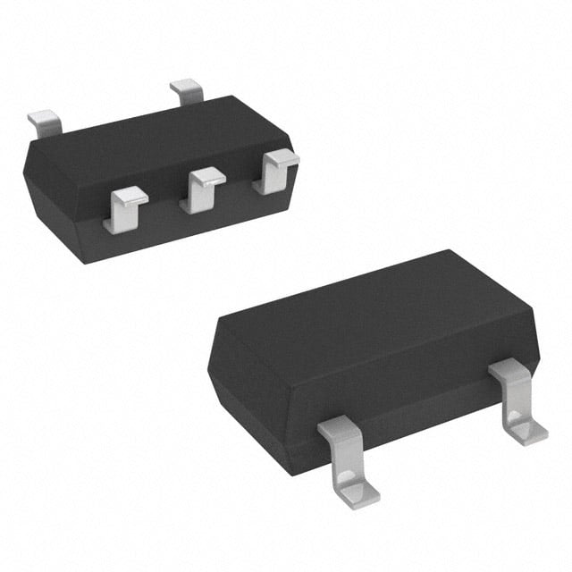
| 描述 | IC OPAMP VFB 350MHZ SC70-5高速运算放大器 Low Pwr 350MHz VTG Feedback |
| 产品分类 | Linear - Amplifiers - Instrumentation, OP Amps, Buffer Amps集成电路 - IC |
| 品牌 | Analog Devices Inc |
| 产品手册 | |
| 产品图片 |
|
| rohs | 符合RoHS无铅 / 符合限制有害物质指令(RoHS)规范要求 |
| 产品系列 | 放大器 IC,高速运算放大器,Analog Devices AD8038AKSZ-REEL7- |
| 数据手册 | |
| 产品型号 | AD8038AKSZ-REEL7 |
| 产品 | Voltage Feedback Amplifier |
| 产品培训模块 | http://www.digikey.cn/PTM/IndividualPTM.page?site=cn&lang=zhs&ptm=30008http://www.digikey.cn/PTM/IndividualPTM.page?site=cn&lang=zhs&ptm=26202 |
| 产品目录页面 | |
| 产品种类 | 高速运算放大器 |
| 供应商器件封装 | SC-70-5 |
| 共模抑制比—最小值 | 65 dB |
| 关闭 | No Shutdown |
| 其它名称 | AD8038AKSZ-REEL7-ND |
| 包装 | 带卷 (TR) |
| 压摆率 | 425 V/µs |
| 商标 | Analog Devices |
| 增益带宽生成 | 80 MHz |
| 增益带宽积 | - |
| 安装类型 | 表面贴装 |
| 安装风格 | SMD/SMT |
| 封装 | Reel |
| 封装/外壳 | 6-TSSOP(5 引线),SC-88A,SOT-353 |
| 封装/箱体 | SC70-5 |
| 工作温度 | -40°C ~ 85°C |
| 工作电源电压 | 3 V to 12 V |
| 工厂包装数量 | 3000 |
| 带宽 | 350 MHz |
| 拓扑结构 | Voltage Feedback |
| 放大器类型 | 电压反馈 |
| 最大工作温度 | + 85 C |
| 最小工作温度 | - 40 C |
| 标准包装 | 3,000 |
| 电压-电源,单/双 (±) | 3 V ~ 12 V, ±1.5 V ~ 6 V |
| 电压-输入失调 | 500µV |
| 电压增益dB | 70 dB |
| 电流-电源 | 1mA |
| 电流-输入偏置 | 400pA |
| 电流-输出/通道 | - |
| 电源电压-最大 | 12 V |
| 电源电压-最小 | 3 V |
| 电源电流 | 1.5 mA |
| 电路数 | 1 |
| 稳定时间 | 18 ns |
| 系列 | AD8038 |
| 视频文件 | http://www.digikey.cn/classic/video.aspx?PlayerID=1364138032001&width=640&height=505&videoID=2245193153001http://www.digikey.cn/classic/video.aspx?PlayerID=1364138032001&width=640&height=505&videoID=2245193159001 |
| 设计资源 | |
| 转换速度 | 425 V/us |
| 输入补偿电压 | 500 uV |
| 输出电流 | 15 mA |
| 输出类型 | - |
| 通道数量 | 1 Channel |


PDF Datasheet 数据手册内容提取
Low Power, 350 MHz Voltage Feedback Amplifiers AD8038/AD8039 FEATURES FUNCTIONAL BLOCK DIAGRAM Low power: 1 mA supply current/amp NC 1 AD8038 8 DISABLE High speed –IN 2 7 +VS 350 MHz, −3 dB bandwidth (G = +1) +IN 3 6 VOUT Lo4w2 c5o Vs/tμ s slew rate –VS N4C = NO CONNECT5 NC 02951-001 Low noise Figure 1. 8-lead SOIC (R) 8 nV/√Hz @ 100 kHz AD8038 600 fA/√Hz @ 100 kHz VOUT 1 5 +VS Low input bias current: 750 nA maximum –VS 2 Low distortion −−9605 ddBB SSFFDDRR @@ 15 MMHHzz +IN 3 4 –IN 02951-002 Figure 2. 5-Lead SC70 (KS) Wide supply range: 3 V to 12 V AD8039 Small packaging: 8-lead SOT-23, 5-lead SC70, and 8-lead SOIC VOUT1 1 8 +VS APPLICATIONS –IN1 2 7 VOUT2 Battery-powered instrumentation +IN1 3 6 –IN2 Filters –VS 4 5 +IN2 ALe/Dve dl rsihviefrtsin g NC = NO CONNECT 02951-003 Buffering Figure 3. 8-Lead SOIC (R) and 8-Lead SOT-23 (RJ) Photo multipliers GENERAL DESCRIPTION The AD8038 (single) and AD8039 (dual) amplifiers are high speed The AD8039 amplifier is available in a 8-lead SOT-23 package, (350 MHz) voltage feedback amplifiers with an exceptionally low and the single AD8038 is available in both an 8-lead SOIC and a quiescent current of 1.0 mA/amplifier typical (1.5 mA maximum). 5-lead SC70 package. These amplifiers are rated to work over The AD8038 single amplifier in the 8-lead SOIC package has a the industrial temperature range of −40°C to +85°C. disable feature. Despite being low power and low cost, the amplifier 24 provides excellent overall performance. Additionally, it offers a 21 G = +10 high slew rate of 425 V/μs and a low input offset voltage of 3 mV 18 maximum. 15 G = +5 The Analog Devices, Inc., proprietary XFCB process allows low 12 noise operation (8 nV/√Hz and 600 fA/√Hz) at extremely low B) d quiescent currents. Given a wide supply voltage range (3 V to 12 V), N ( 9 AI G = +2 wide bandwidth, and small packaging, the AD8038 and AD8039 G 6 amplifiers are designed to work in a variety of applications 3 where power and space are at a premium. G = +1 0 The AD8038 and AD8039 amplifiers have a wide input common- –3 mode range of 1 V from either rail and swing to within 1 V of each rcaapila ocniti vthe elo oaudtsp uupt .t oT h15e speF a. Imf dprliivfiienrgs laarrgee or pctaipmaciziteivde f loora ddsr,i va isnmg all –60.1 1 FREQUEN10CY (MHz) 100 1000 02951-004 Figure 4. Small Signal Frequency Response for Various Gains, series resistor is needed to avoid excessive peaking or overshoot. VOUT = 500 mV p-p, VS = ±5 V Rev. G Information furnished by Analog Devices is believed to be accurate and reliable. However, no responsibility is assumed by Analog Devices for its use, nor for any infringements of patents or other One Technology Way, P.O. Box 9106, Norwood, MA 02062-9106, U.S.A. rights of third parties that may result from its use. Specifications subject to change without notice. No license is granted by implication or otherwise under any patent or patent rights of Analog Devices. Tel: 781.329.4700 www.analog.com Trademarks and registered trademarks are the property of their respective owners. Fax: 781.461.3113 ©2002–2009 Analog Devices, Inc. All rights reserved.
AD8038/AD8039 TABLE OF CONTENTS Features .............................................................................................. 1 Disable ......................................................................................... 13 Applications ....................................................................................... 1 Power Supply Bypassing ............................................................ 13 Functional Block Diagram .............................................................. 1 Grounding ................................................................................... 13 General Description ......................................................................... 1 Input Capacitance ...................................................................... 13 Revision History ............................................................................... 2 Output Capacitance ................................................................... 13 Specifications ..................................................................................... 3 Input-to-Output Coupling ........................................................ 13 Absolute Maximum Ratings ............................................................ 5 Applications Information .............................................................. 14 Maximum Power Dissipation ..................................................... 5 Low Power ADC Driver ............................................................ 14 Output Short Circuit .................................................................... 5 Low Power Active Video Filter ................................................. 14 ESD Caution .................................................................................. 5 Outline Dimensions ....................................................................... 15 Typical Performance Characteristics ............................................. 6 Ordering Guide .......................................................................... 16 Layout, Grounding, and Bypassing Considerations .................. 13 REVISION HISTORY 8/09—Rev. F to Rev. G 5/02—Rev. A to Rev. B Changes to Applications Section and General Description Add Part Number AD8038 ............................................... Universal Section ................................................................................................ 1 Changes to Product Title .................................................................. 1 Changes to Disable Section and Grounding Section ................. 13 Changes to Features .......................................................................... 1 Changes to Low Power ADC Driver Section and Low Power Changes to Product Description ..................................................... 1 Active Video Filter Section ............................................................ 14 Changes to Connection Diagram .................................................... 1 Updated Outline Dimensions ....................................................... 15 Update to Specifications ................................................................... 2 Changes to Ordering Guide .......................................................... 16 Update to Maximum Power Dissipation ........................................ 4 Update to Output Short Circuit ....................................................... 4 8/04—Rev. E to Rev. F Update to Ordering Guide ............................................................... 4 Changes to Figure 4 ........................................................................ 10 Change to Figure 2 ............................................................................ 4 8/03—Rev. D to Rev. E Change to TPC 2 ............................................................................... 5 Change to TPC 18 ............................................................................. 6 Change to TPC 34............................................................................. 8 Change to TPC 27 ............................................................................. 7 7/03—Rev. C to Rev. D Change to TPC 29 ............................................................................. 8 Changes to Ordering Guide ............................................................ 4 Change to TPC 30 ............................................................................. 8 Updated TPC 35 Caption ................................................................ 8 Change to TPC 31 ............................................................................. 8 Added TPC 36 .................................................................................... 8 6/03—Rev. B to Rev. C Added TPC 37 .................................................................................... 9 Updated Connection Diagrams ...................................................... 1 Edits to Low Power Active Video Filter ....................................... 10 Updated Ordering Guide ................................................................. 4 Change to Figure 4 ......................................................................... 10 Updated Outline Dimensions ....................................................... 11 4/02—Rev. 0 to Rev. A Changes to Features .......................................................................... 1 Update Specifications ................................................................... 2, 3 Edits to TPC 19 .................................................................................. 7 Rev. G | Page 2 of 16
AD8038/AD8039 SPECIFICATIONS T = 25°C, V = ±5 V, R = 2 kΩ, Gain = +1, unless otherwise noted. A S L Table 1. Parameter Conditions Min Typ Max Unit DYNAMIC PERFORMANCE −3 dB Bandwidth G = +1, V = 0.5 V p-p 300 350 MHz O G = +2, V = 0.5 V p-p 175 MHz O G = +1, V = 2 V p-p 100 MHz O Bandwidth for 0.1 dB Flatness G = +2, V = 0.2 V p-p 45 MHz O Slew Rate G = +1, V = 2 V step, R = 2 kΩ 400 425 V/μs O L Overdrive Recovery Time G = +2, 1 V overdrive 50 ns Settling Time to 0.1% G = +2, V = 2 V step 18 ns O NOISE/HARMONIC PERFORMANCE SFDR Second Harmonic f = 1 MHz, V = 2 V p-p, R = 2 kΩ −90 dBc C O L Third Harmonic f = 1 MHz, V = 2 V p-p, R = 2 kΩ −92 dBc C O L Second Harmonic f = 5 MHz, V = 2 V p-p, R = 2 kΩ −65 dBc C O L Third Harmonic f = 5 MHz, V = 2 V p-p, R = 2 kΩ −70 dBc C O L Crosstalk, Output-to-Output (AD8039) f = 5 MHz, G = +2 −70 dB Input Voltage Noise f = 100 kHz 8 nV/√Hz Input Current Noise f = 100 kHz 600 fA/√Hz DC PERFORMANCE Input Offset Voltage 0.5 3 mV Input Offset Voltage Drift 4.5 μV/°C Input Bias Current 400 750 nA Input Bias Current Drift 3 nA/°C Input Offset Current ±25 nA Open-Loop Gain V = ±2.5 V 70 dB O INPUT CHARACTERISTICS Input Resistance 10 MΩ Input Capacitance 2 pF Input Common-Mode Voltage Range R = 1 kΩ ±4 V L Common-Mode Rejection Ratio V = ±2.5 V 61 67 dB CM OUTPUT CHARACTERISTICS DC Output Voltage Swing R = 2 kΩ, saturated output ±4 V L Capacitive Load Drive 30% overshoot, G = +2 20 pF POWER SUPPLY Operating Range 3.0 12 V Quiescent Current per Amplifier 1.0 1.5 mA Power Supply Rejection Ratio −Supply −71 −77 dB +Supply −64 −70 dB POWER-DOWN DISABLE1 Turn-On Time 180 ns Turn-Off Time 700 ns Disable Voltage—Part is Off +V − 4.5 V S Disable Voltage—Part is On +V − 2.5 V S Disabled Quiescent Current 0.2 mA Disabled In/Out Isolation f = 1 MHz −60 dB 1 Only available in AD8038 8-lead SOIC package. Rev. G | Page 3 of 16
AD8038/AD8039 T = 25°C, V = 5 V, R = 2 kΩ to V/2, Gain = +1, unless otherwise noted. A S L S Table 2. Parameter Conditions Min Typ Max Unit DYNAMIC PERFORMANCE −3 dB Bandwidth G = +1, V = 0.2 V p-p 275 300 MHz O G = +2, V = 0.2 V p-p 150 MHz O G = +1, V = 2 V p-p 30 MHz O Bandwidth for 0.1 dB Flatness G = +2, V = 0.2 V p-p 45 MHz O Slew Rate G = +1, V = 2 V step, R = 2 kΩ 340 365 V/μs O L Overdrive Recovery Time G = +2, 1 V overdrive 50 ns Settling Time to 0.1% G = +2, V = 2 V step 18 ns O NOISE/HARMONIC PERFORMANCE SFDR Second Harmonic f = 1 MHz, V = 2 V p-p, R = 2 kΩ −82 dBc C O L Third Harmonic f = 1 MHz, V = 2 V p-p, R = 2 kΩ −79 dBc C O L Second Harmonic f = 5 MHz, V = 2 V p-p, R = 2 kΩ −60 dBc C O L Third Harmonic f = 5 MHz, V = 2 V p-p, R = 2 kΩ −67 dBc C O L Crosstalk, Output-to-Output f = 5 MHz, G = +2 −70 dB Input Voltage Noise f = 100 kHz 8 nV/√Hz Input Current Noise f = 100 kHz 600 fA/√Hz DC PERFORMANCE Input Offset Voltage 0.8 3 mV Input Offset Voltage Drift 3 μV/°C Input Bias Current 400 750 nA Input Bias Current Drift 3 nA/°C Input Offset Current ±30 nA Open-Loop Gain V = ±2.5 V 70 dB O INPUT CHARACTERISTICS Input Resistance 10 MΩ Input Capacitance 2 pF Input Common-Mode Voltage Range R = 1 kΩ 1.0 − 4.0 V L Common-Mode Rejection Ratio V = ±1 V 59 65 dB CM OUTPUT CHARACTERISTICS DC Output Voltage Swing R = 2 kΩ, saturated output 0.9 − 4.1 V L Capacitive Load Drive 30% overshoot 20 pF POWER SUPPLY Operating Range 3 12 V Quiescent Current per Amplifier 0.9 1.5 mA Power Supply Rejection Ratio −65 −71 dB POWER-DOWN DISABLE1 Turn-On Time 210 ns Turn-Off Time 700 ns Disable Voltage—Part is Off +V − 4.5 V S Disable Voltage—Part is On +V − 2.5 V S Disabled Quiescent Current 0.2 mA Disabled In/Out Isolation f = 1 MHz −60 dB 1 Only available in AD8038 8-lead SOIC package. Rev. G | Page 4 of 16
AD8038/AD8039 ABSOLUTE MAXIMUM RATINGS 2.0 Table 3. Parameter Rating W) Supply Voltage 12.6 V ON ( 1.5 Power Dissipation See Figure 5 ATI SOIC-8 P Common-Mode Input Voltage ±V SI S S SOT-23-8 DI Differential Input Voltage ±4 V R 1.0 E Storage Temperature Range −65°C to +125°C W SC70-5 O Operating Temperature Range −40°C to +85°C M P U Lead Temperature (Soldering, 10 sec) 300°C M 0.5 XI A M Stresses above those listed under Absolute Maximum Ratings mrataiyn gca ounsley p; feurmncatnioennat ld oapmeraagteio tno othf et hdee vdiecvei.c Te haits t ihse as es torre sasn y 0–55 –25 AM5BIENT TE3M5PERATU6R5E(°C) 95 125 02951-005 other conditions above those indicated in the operational Figure 5. Maximum Power Dissipation vs. Temperature for a 4-Layer Board section of this specification is not implied. Exposure to absolute RMS output voltages should be considered. If R is referenced to L maximum rating conditions for extended periods may affect V , as in single-supply operation, then the total drive power is S− device reliability. V × I . If the rms signal levels are indeterminate, consider the S OUT MAXIMUM POWER DISSIPATION worst case, when VOUT = VS /4 for RL to midsupply The maximum safe power dissipation in the AD8038/AD8039 PD = (VS × IS) + (VS/4)2/RL package is limited by the associated rise in junction temperature In single-supply operation with R referenced to V , worst case L S− (TJ) on the die. The plastic encapsulating the die locally reaches is VOUT = VS /2. the junction temperature. At approximately 150°C, which is the Airflow increases heat dissipation, effectively reducing θ . In glass transition temperature, the plastic changes its properties. JA addition, more metal directly in contact with the package leads Even temporarily exceeding this temperature limit may change from metal traces, throughholes, ground, and power planes reduce the stresses that the package exerts on the die, permanently the θ . Care must be taken to minimize parasitic capacitances at shifting the parametric performance of the AD8038/AD8039. JA the input leads of high speed op amps as discussed in the Exceeding a junction temperature of 175°C for an extended Layout, Grounding, and Bypassing Considerations section. time can result in changes in the silicon devices, potentially causing failure. Figure 5 shows the maximum safe power dissipation in the package vs. the ambient temperature for the 8-lead SOIC The still-air thermal properties of the package and PCB (θ ), JA (125°C/W), 5-lead SC70 (210°C/W), and 8-lead SOT-23 ambient temperature (T ), and total power dissipated in the A (160°C/W) packages on a JEDEC standard 4-layer board. package (P ) determine the junction temperature of the die. D θ values are approximations. The junction temperature can be calculated as JA OUTPUT SHORT CIRCUIT T = T + (P × θ ) J A D JA Shorting the output to ground or drawing excessive current The power dissipated in the package (P ) is the sum of the D from the AD8038/AD8039 will likely cause a catastrophic failure. quiescent power dissipation and the power dissipated in the package due to the load drive for all outputs. The quiescent power is the voltage between the supply pins (VS) multiplied by the ESD CAUTION quiescent current (I). Assuming the load (R) is referenced to S L midsupply, then the total drive power is V/2 × I , some of which S OUT is dissipated in the package and some in the load (V × I ). OUT OUT The difference between the total drive power and the load power is the drive power dissipated in the package. P = quiescent power + (total drive power − load power) D P = [V × I] + [(V/2) × (V /R)] − [V 2/R] D S S S OUT L OUT L Rev. G | Page 5 of 16
AD8038/AD8039 TYPICAL PERFORMANCE CHARACTERISTICS Default Conditions: ±5 V, C = 5 pF, G = +2, R = R = 1 kΩ, R = 2 kΩ, V = 2 V p-p, Frequency = 1 MHz, T = 25°C. L G F L O A 24 7 21 G = +10 RL = 2kΩ 6 18 15 G = +5 5 RL = 500Ω 12 B) B) 4 d d N ( 9 N ( GAI 6 G = +2 GAI 3 3 2 RL = 1kΩ G = +1 0 1 –3 –6 0 0.1 1 FREQUE1N0CY (MHz) 100 1000 02951-006 0.1 1 FREQUE1N0CY (MHz) 100 1000 02951-009 Figure 6. Small Signal Frequency Response for Various Gains, Figure 9. Small Signal Frequency Response for Various RL, VOUT = 500 mV p-p VS = 5 V, VOUT = 500 mV p-p 7 8 VS = ±1.5V 6 RL = 2kΩ VS = ±2.5V 7 5 6 VS = ±5V RL = 500Ω B) 4 5 N (d dB) GAI 3 AIN ( 4 G 3 2 RL = 1kΩ 2 1 1 0 Fig0u.r1e 7. Small Sig1nal FrFeqRuEQenUcEy1N 0RCeYs p(MoHnzs)e for1 V00arious Supp1li0e0s0, 02951-007 00.1 1FREQUENCY (MHz)10 100 02951-010 VOUT = 500 mV p-p Figure 10. Large Signal Frequency Response for Various RL, VOUT = 3 V p-p, VS = 5 V 7 8 RL = 2kΩ 6 7 RL = 2kΩ 5 6 dB) 4 B) 5 RL = 500Ω GAIN ( 3 AIN (d 4 G RL = 500Ω 3 2 RL = 1kΩ RL = 1kΩ 2 1 1 0 0F.i1gure 8. SmallV 1SSi =gn ±a5Fl FRVrE, eVQqOUuUEeT 1Nn=0Cc 5yY0 R(0Me msHpzVo) nps-pe1 f0o0r Various RL1, 0 00 02951-008 0F0i.g1ure 11. Large SVigOnU1Ta F=l RF 4Er eQVq UpuE-epNn,C cVYyS (R=Me H±spz5)1o V0n se for Various RL1, 0 0 02951-011 Rev. G | Page 6 of 16
AD8038/AD8039 5 80 180 4 CL = 15pF 70 3 60 135 CL = 10pF 2 B) 50 GAIN (dB) –110 CL = 5pF EN-LOOP GAIN (d 234000 GAINPHASE 9405 PHASE (Degrees) –2 OP 10 –3 0 0 –4 –10 –5 –20 –45 1 10FREQUENCY (MHz1)00 1000 02951-012 0.01 0.1 FRE1QUENCY (M10Hz) 100 1000 02951-015 Figure 12. Small Signal Frequency Response for Various CL, Figure 15. Open-Loop Gain and Phase, VS = ±5 V VOUT = 500 mV p-p, VS = ±5 V, G = +1 9 7 CL = 15pF 5 6 –40°C 3 CL = 10pF B) +25°C N (dB) 1 AIN (d 3 AI G G –1 CL = 5pF +85°C 0 –3 –3 –51 10FREQUENCY (MHz1)00 1000 02951-013 0.1 Figure 16. F1requeFnRcEyQ RUeEs1Np0CoYn s(Me Hvzs). Tem1p00erature, 1000 02951-016 Figure 13. SmVOaUlTl S=i g5n0a0 lm FrVe qpu-pe,n VcSy = R 5es Vp,o Gn =se + fo1r Various CL, Gain = +2, VS = ±5 V, VOUT = 2 V p-p 2 –50 1 VOUT = 200mV –55 RL = 500Ω HD2 VOUT = 1V c) RL = 500Ω HD3 0 dB –60 N ( –1 TIO –65 B) OR GAIN (d ––32 VOUT = 500mV ONIC DIST ––7750 RL = 2kΩ HD2 RL = 2kΩ HD3 –4 VOUT = 2V ARM –80 H –5 –85 –60.1 1 FREQUE1N0CY (MHz) 100 1000 02951-014 –901 2 3 4FREQ5UENCY6 (MHz)7 8 9 10 02951-017 Figure 14. Frequency Response for Various Output Voltage Levels Figure 17. Harmonic Distortion vs. Frequency for Various Loads, VS = ±5 V, VOUT = 2 V p-p, G = +2 Rev. G | Page 7 of 16
AD8038/AD8039 –45 –40 –50 10MHz HD2 RL = 500Ω HD2 –50 N (dBc) ––6505 RL = 500Ω HD3 N (dBc) –60 10MHz HD3 5MHz HD2 O O TI TI OR –65 OR 5MHz HD3 ST ST –70 DI –70 DI NIC RL = 2kΩ HD3 NIC 1MHz HD3 O –75 O –80 M M HAR –80 RL = 2kΩ HD2 HAR 1MHz HD2 –90 –85 –90 –100 1 2 3 4FREQ5UENCY6 (MHz)7 8 9 10 02951-018 1 2AMPLITUDE (V p-p)3 4 02951-021 Figure 18. Harmonic Distortion vs. Frequency for Various Loads, Figure 21. Harmonic Distortion vs. VOUT Amplitude for Various Frequencies, VS = 5 V, VOUT = 2 V p-p, G = +2 VS = ±5 V, G = +2 –50 –45 10MHz HD2 G = +1 HD2 c) –60 c) –55 10MHz HD3 N (dB G = +2 HD2 N (dB 5MHz HD2 O O TI –70 TI –65 R R O O DIST G = +2 HD3 DIST 5MHz HD3 C –80 C –75 ONI ONI 1MHz HD3 M M R G = +1 HD3 R A A 1MHz HD2 H –90 H –85 –100 –95 1 2 3 4FREQ5UENCY6 (MHz)7 8 9 10 02951-019 1.0 1.5 AMPLITU2D.0E (V p-p) 2.5 3.0 02951-022 Figure 19. Harmonic Distortion vs. Frequency for Various Gains, Figure 22. Harmonic Distortion vs. Amplitude for Various Frequencies, VS = ±5 V, VOUT = 2 V p-p VS = 5 V, G = +2 1000 –50 G = +1 HD2 c) –60 Hz) ON (dB G = +2 HD2 E (nV/ 100 RTI –70 OIS O N MONIC DIST –80 G = +2 HD3 VOLTAGE 10 R HA –90 G = +1 HD3 1 –1001 2 3 4FREQU5ENCY6 (MHz)7 8 9 10 02951-020 10 F1ig0u0re 23.1 IknputF VR1oE0QltkaUgEeN CN1Yo0 0i(sHkez )vs. F1rMequen1c0yM 100M 02951-023 Figure 20. Harmonic Distortion vs. Frequency for Various Gains, VS = 5 V, VOUT = 2 V p-p Rev. G | Page 8 of 16
AD8038/AD8039 100k CL = 25pF WITH RSNUB = 19.6Ω 10k Hz) √ A/ E (f S OI CL = 5pF N 1k CL = 10pF 100 50mV/DIV 5ns/DIV 10 100 FR1kEQUENCY 1(H0kz) 100k 1M 02951-024 02951-027 Figure 24. Input Current Noise vs. Frequency Figure 27. Small Signal Transient Response for Various CL, VS = 5 V RL = 500Ω RL = 2kΩ CL = 25pF WITH RSNUB = 19.6Ω CL = 5pF CL = 10pF 50mV/DIV 5ns/DIV 02951-025 50mV/DIV 5ns/DIV 02951-028 Figure 25. Small Signal Transient Response for Various RL, VS = 5 V Figure 28. Small Signal Transient Response for Various CL, VS = ±5 V RL = 500Ω RL = 2kΩ RL = 500Ω RL = 2kΩ 2.5V 50mV/DIV 5ns/DIV 500mV/DIV 5ns/DIV 02951-026 02951-029 Figure 26. Small Signal Transient Response for Various RL, VS = ±5 V Figure 29. Large Signal Transient Response for Various RL, VS = 5 V Rev. G | Page 9 of 16
AD8038/AD8039 RL = 2kΩ IN RL = 500Ω OUT 1V/DIV 5ns/DIV 02951-030 2V/DIV 50ns/DIV 02951-033 Figure 30. Large Signal Transient Response for Various RL, VS = ±5 V Figure 33. Input Overdrive Recovery, Gain = +1 CL = 25pF IN OUT CL = 5pF 2.5V 500mV/DIV 5ns/DIV 02951-031 IONUPTUPTU 1TV 2/DVI/VDIV 50ns/DIV 02951-034 Figure 31. Large Signal Transient Response for Various CL, VS = 5 V Figure 34. Output Overdrive Recovery, Gain = +2 CL = 10pF 2mV/DIV VS = ±5V G = +2 VOUT= 2V p-p CL = 5pF ERROR VOLTAGE +0.1% 0 t = 0 –0.1% VIN 500mV/DIV 5ns/DIV 02951-032 0.5V/DIV 5ns/DIV 02951-035 Figure 32. Large Signal Transient Response for Various CL, VS = ±5 V Figure 35. 0.1% Settling Time VOUT = 2 V p-p Rev. G | Page 10 of 16
AD8038/AD8039 –10 10 –20 0 –30 –10 –20 B) –40 –PSRR d K ( –50 B) –30 L d TA SIDE B R ( –40 OSS –60 SIDE A PSR –50 +PSRR R C –70 –60 –80 –70 –90 –80 –1000.1 1 FREQUE1N0CY (MHz) 100 1000 02951-036 –900.01 0.1 FRE1QUENCY (M10Hz) 100 1000 02951-039 Figure 36. AD8039 Crosstalk, VIN = 1 V p-p, Gain = +1 Figure 39. PSRR vs. Frequency 9 –10 8 VS = ±5V –20 7 –30 6 RR (dB) –40 VS = +5V VS = ±5V V (p-p)OUT 45 CM –50 3 VS = +5V –60 2 –70 1 0 –801 10FREQUENCY (MHz1)00 1000 02951-037 0 Figur1e0 400. Outpu2t0 S0RwLiOnAgD v (sΩ. )3L0o0ad Resist4a0n0ce 500 02951-040 Figure 37. CMRR vs. Frequency, VIN = 1 V p-p 1000 1.25 1.00 100 A) m IMPEDANCEΩ) 10 PPLY CURRENT ( 00..7550 U 1 S VS = ±5V 0.25 VS = +5V 0.1 0 0.01 0.1 FRE1QUENCY (M10Hz) 100 1000 02951-038 0 2 4SUPPLY VO6LTAGE (V8) 10 12 02951-041 Figure 38. Output Impedance vs. Frequency Figure 41. AD8038 Supply Current vs. Supply Voltage Rev. G | Page 11 of 16
AD8038/AD8039 0 –10 –20 –30 B) d N ( –40 O TI A –50 L O S I –60 –70 –80 –90 0.1 1 FREQUE1N0CY (MHz) 100 1000 02951-042 Figure 42. AD8038 Input-Output Isolation (G = +2, RL = 2 kΩ, VS = ±5 V) Rev. G | Page 12 of 16
AD8038/AD8039 LAYOUT, GROUNDING, AND BYPASSING CONSIDERATIONS DISABLE INPUT CAPACITANCE The AD8038 in the 8-lead SOIC package provides a disable Along with bypassing and ground, high speed amplifiers can be feature. This feature disables the input from the output (see sensitive to parasitic capacitance between the inputs and ground. A Figure 42 for input-output isolation) and reduces the quiescent few picofarads of capacitance reduces the input impedance at current from typically 1 mA to 0.2 mA. When the DISABLE high frequencies, in turn increasing the gain of the amplifiers, node is pulled below 4.5 V from the positive supply rail, the part causing peaking of the frequency response, or even oscillations becomes disabled. To enable the part, the DISABLE node needs if severe enough. It is recommended that the external passive to be pulled to greater than (V – 2.5). components that are connected to the input pins be placed as S close as possible to the inputs to avoid parasitic capacitance. POWER SUPPLY BYPASSING The ground and power planes must be kept at a distance of at Power supply pins are actually inputs, and care must be taken least 0.05 mm from the input pins on all layers of the board. so that a noise-free stable dc voltage is applied. The purpose of OUTPUT CAPACITANCE bypass capacitors is to create low impedances from the supply to ground at all frequencies, thereby shunting or filtering a To a lesser extent, parasitic capacitances on the output can cause majority of the noise. peaking of the frequency response. Two methods to minimize this effect include the following: Decoupling schemes are designed to minimize the bypassing impedance at all frequencies with a parallel combination of • Put a small value resistor in series with the output to isolate capacitors. The 0.01 μF or 0.001 μF (X7R or NPO) chip capacitors the load capacitor from the output stage of the amplifier, see are critical and should be placed as close as possible to the Figure 12, Figure 13, Figure 27, and Figure 28. amplifier package. Larger chip capacitors, such as 0.1 μF • Increase the phase margin with higher noise gains or add capacitors, can be shared among a few closely spaced active a pole with a parallel resistor and capacitor from −IN to components in the same signal path. A 10 μF tantalum capacitor the output. is less critical for high frequency bypassing and, in most cases, INPUT-TO-OUTPUT COUPLING only one per board is needed at the supply inputs. The input and output signal traces should not be parallel to GROUNDING minimize capacitive coupling between the inputs and outputs, A ground plane layer is important in densely packed PC boards avoiding any positive feedback. to spread the current minimizing parasitic inductances. However, an understanding of where the current flows in a circuit is critical to implementing effective high speed circuit design. The length of the current path is directly proportional to the magnitude of parasitic inductances and, therefore, the high frequency impedance of the path. High speed currents in an inductive ground return create an unwanted voltage noise. The length of the high frequency bypass capacitor leads is most critical. A parasitic inductance in the bypass grounding works against the low impedance created by the bypass capacitor. Because load currents flow from the supplies as well, the ground for the load impedance should be at the same physical location as the bypass capacitor grounds. For the larger value capacitors, which are intended to be effective at lower frequencies, the current return path distance is less critical. Rev. G | Page 13 of 16
AD8038/AD8039 APPLICATIONS INFORMATION LOW POWER ADC DRIVER LOW POWER ACTIVE VIDEO FILTER 1kΩ 2.5V Some composite video signals derived from a digital source +5V 0.1µF 10µF contain clock feedthrough that can limit picture quality. Active 3V filters made from op amps can be used in this application, but 0.1µF 10µF they consume 25 mW to 30 mW for each channel. In power- 1kΩ 3 8 REF sensitive applications, this can be too much, requiring the use 1 50Ω 0V VIN 2 VINP of passive filters that can create impedance matching problems 1kΩ when driving any significant load. 1kΩ AD9203 AD8039 The AD8038 can be used to make an effective low-pass active 1kΩ 6 1kΩ filter that consumes one-fifth of the power consumed by an 7 50Ω VINN active filter made from an op amp. Figure 44 shows a circuit 5 4 that uses a AD8038 with ±2.5 V supplies to create a three-pole 1kΩ Sallen-Key filter. This circuit uses a single RC pole in front of a 0.1µF 10µF standard 2-pole active section. Figure 43. Schem–a5Vtic to D1rkiΩve AD9203 with the AD8039 02951-043 680pF 1RΩF +2.5V The AD9203 is a low power (125 mW on a 5 V supply), 40 MSPS 10-bit converter. As such, the low power, high performance 0.1µF 10µF AD8039 is an appropriate amplifier choice to drive it. 20R01Ω 49R92Ω 49R.93Ω AD8038 VOUT In low supply voltage applications, differential analog inputs VIN R755Ω R4 C1 C3 aDrief fnereeendteiadl tdor iivnincrge caasne tahlseo d ryednuacme isce rcaonngde a onfd t hoteh AerD eCve nin-pourdtse.r 49.9Ω 100pF 33pF –2.5V 0.1µF 10µF 02951-044 distortion products. The AD8039 can be used to make a dc- Figure 44. Low-Pass Filter for Video coupled, single-ended-to-differential driver for driving these Figure 45 shows the frequency response of this filter. The ADCs. Figure 43 is a schematic of such a circuit for driving the response is down 3 dB at 6 MHz; therefore, it passes the video AD9203, 10-bit, 40 MSPS ADC. band with little attenuation. The rejection at 27 MHz is 45 dB, The AD9203 works best when the common-mode voltage at the which provides more than a factor of 100 in suppression of the input is at the midsupply or 2.5 V. The output stage design of clock components at this frequency. the AD8039 makes it ideal for driving these types of ADCs. 10 In this circuit, one of the op amps is configured in the inverting 0 mode, and the other is in the noninverting mode. However, to provide better bandwidth matching, each op amp is configured –10 for a noise gain of +2. The inverting op amp is configured for a gain of −1, and the noninverting op amp is configured for a gain dB) –20 of +2. Each has a very similar ac response. The input signal to GAIN ( –30 the noninverting op amp is divided by 2 to normalize its voltage level and make it equal to the inverting output. –40 The outputs of the op amps are centered at 2.5 V, which is the –50 midsupply level of the ADC. This is accomplished by first taking the 2.5 V reference output of the ADC and dividing it by 2 with –60 ap opsaiitriv oef i1n pkuΩt orefs eisatcohr so. pT ahme pre. sTuhltiisn vgo 1lt.2ag5e V is i st haepnp lmieudl ttiop ltiheed by 0.1 1FREQUENCY (MHz)10 100 02951-045 Figure 45. Video Filter Response the gain of the op amps to provide a 2.5 V level at each output. Rev. G | Page 14 of 16
AD8038/AD8039 OUTLINE DIMENSIONS 5.00(0.1968) 4.80(0.1890) 8 5 4.00 (0.1574) 6.20 (0.2441) 3.80 (0.1497) 1 4 5.80 (0.2284) 1.27 (0.0500) 0.50 (0.0196) BSC 1.75 (0.0688) 0.25 (0.0099) 45° 0.25 (0.0098) 1.35 (0.0532) 8° 0.10 (0.0040) 0° COPLANARITY 0.51 (0.0201) 0.10 SEATING 0.31 (0.0122) 0.25 (0.0098) 10..2470 ((00..00510507)) PLANE 0.17 (0.0067) COMPLIANTTO JEDEC STANDARDS MS-012-AA C(RINOEFNPETARRREOENNLCLTEIHN EOGSN DELSIYM)AEANNRDSEI AORRNOESU NANORDEET DAIN-PO MPFRIFLO LMPIIMRLELIATIMTEEER TFSEO; RIRN ECUQHSU EDI VIINMA LEDENENSSTIIOGSN NFS.OR 012407-A Figure 46. 8-Lead Standard Small Outline Package [SOIC_N] Narrow Body (R-8) Dimensions shown in millimeters and (inches) 2.20 2.00 1.80 1.35 5 4 2.40 1.25 2.10 1.15 1 2 3 1.80 PIN1 0.65 BSC 1.00 0.40 1.10 0.90 0.10 0.80 0.70 0.46 0.10 MAX 0.30 0.22 0.36 0.15 SEATING 0.08 0.26 PLANE 0.10 COPLANARITY COMPLIANT TO JEDEC STANDARDS MO-203-AA Figure 47. 5-Lead Thin Shrink Small Outline Transistor Package [SC70] (KS-5) Dimensions shown in millimeters Rev. G | Page 15 of 16
AD8038/AD8039 3.00 2.90 2.80 1.70 8 7 6 5 3.00 1.60 2.80 1.50 2.60 1 2 3 4 PIN 1 INDICATOR 0.65 BSC 1.95 BSC 1.30 1.15 0.90 1.45 MAX 0.22 MAX 0.95 MIN 0.08 MIN 0.60 0.15 MAX 8° 0.45 0.05 MIN 0.38 MAX SPELAATNIENG 4° B0S.6C0 0.30 0.22 MIN 0° COMPLIANT TO JEDEC STANDARDS MO-178-BA 121608-A Figure 48. 8-Lead Small Outline Transistor Package [SOT-23] (RJ-8) Dimensions shown in millimeters ORDERING GUIDE Model Temperature Range Package Description Package Option Branding AD8038AR −40°C to +85°C 8-Lead Standard Small Outline Package [SOIC_N] R-8 AD8038AR-REEL −40°C to +85°C 8-Lead Standard Small Outline Package [SOIC_N] R-8 AD8038AR-REEL7 −40°C to +85°C 8-Lead Standard Small Outline Package [SOIC_N] R-8 AD8038ARZ1 −40°C to +85°C 8-Lead Standard Small Outline Package [SOIC_N] R-8 AD8038ARZ-REEL1 −40°C to +85°C 8-Lead Standard Small Outline Package [SOIC_N] R-8 AD8038ARZ-REEL71 −40°C to +85°C 8-Lead Standard Small Outline Package [SOIC_N] R-8 AD8038AKSZ-R21 −40°C to +85°C 5-Lead Thin Shrink Small Outline Transistor Package [SC70] KS-5 H1C AD8038AKSZ-REEL1 −40°C to +85°C 5-Lead Thin Shrink Small Outline Transistor Package [SC70] KS-5 H1C AD8038AKSZ-REEL71 −40°C to +85°C 5-Lead Thin Shrink Small Outline Transistor Package [SC70] KS-5 H1C AD8039AR −40°C to +85°C 8-Lead Standard Small Outline Package [SOIC_N] R-8 AD8039AR-REEL −40°C to +85°C 8-Lead Standard Small Outline Package [SOIC_N] R-8 AD8039AR-REEL7 −40°C to +85°C 8-Lead Standard Small Outline Package [SOIC_N] R-8 AD8039ARZ1 −40°C to +85°C 8-Lead Standard Small Outline Package [SOIC_N] R-8 AD8039ARZ-REEL1 −40°C to +85°C 8-Lead Standard Small Outline Package [SOIC_N] R-8 AD8039ARZ-REEL71 −40°C to +85°C 8-Lead Standard Small Outline Package [SOIC_N] R-8 AD8039ART-R2 −40°C to +85°C 8-Lead Small Outline Transistor Package [SOT-23] RJ-8 HYA AD8039ART-REEL −40°C to +85°C 8-Lead Small Outline Transistor Package [SOT-23] RJ-8 HYA AD8039ART-REEL7 −40°C to +85°C 8-Lead Small Outline Transistor Package [SOT-23] RJ-8 HYA AD8039ARTZ-R21 −40°C to +85°C 8-Lead Small Outline Transistor Package [SOT-23] RJ-8 HYA# AD8039ARTZ-REEL1 −40°C to +85°C 8-Lead Small Outline Transistor Package [SOT-23] RJ-8 HYA# AD8039ARTZ-REEL71 −40°C to +85°C 8-Lead Small Outline Transistor Package [SOT-23] RJ-8 HYA# 1 Z = RoHS Compliant Part, # denotes RoHS compliant part may be top or bottom marked.. ©2002–2009 Analog Devices, Inc. All rights reserved. Trademarks and registered trademarks are the property of their respective owners. D02951-0-8/09(G) Rev. G | Page 16 of 16
Mouser Electronics Authorized Distributor Click to View Pricing, Inventory, Delivery & Lifecycle Information: A nalog Devices Inc.: AD8038ARZ AD8038ARZ-REEL7 AD8038ARZ-REEL AD8038AKSZ-REEL7 AD8038AKSZ-R2