ICGOO在线商城 > 集成电路(IC) > 数据采集 - 模数转换器 > AD7995YRJZ-0500RL7
 Datasheet下载
- 型号: AD7995YRJZ-0500RL7
- 制造商: Analog
- 库位|库存: xxxx|xxxx
- 要求:
| 数量阶梯 | 香港交货 | 国内含税 |
| +xxxx | $xxxx | ¥xxxx |
查看当月历史价格
查看今年历史价格
AD7995YRJZ-0500RL7产品简介:
ICGOO电子元器件商城为您提供AD7995YRJZ-0500RL7由Analog设计生产,在icgoo商城现货销售,并且可以通过原厂、代理商等渠道进行代购。 AD7995YRJZ-0500RL7价格参考。AnalogAD7995YRJZ-0500RL7封装/规格:数据采集 - 模数转换器, 10 Bit Analog to Digital Converter 3, 4 Input 1 SAR SOT-23-8。您可以下载AD7995YRJZ-0500RL7参考资料、Datasheet数据手册功能说明书,资料中有AD7995YRJZ-0500RL7 详细功能的应用电路图电压和使用方法及教程。
| 参数 | 数值 |
| 产品目录 | 集成电路 (IC)半导体 |
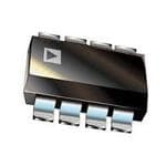
| 描述 | IC ADC 10BIT 4CH SAR I2C SOT23-8模数转换器 - ADC 4CH 10-Bit w/ I2C Compatible IF |
| 产品分类 | |
| 品牌 | Analog Devices |
| 产品手册 | |
| 产品图片 |
|
| rohs | 符合RoHS无铅 / 符合限制有害物质指令(RoHS)规范要求 |
| 产品系列 | 数据转换器IC,模数转换器 - ADC,Analog Devices AD7995YRJZ-0500RL7- |
| 数据手册 | |
| 产品型号 | AD7995YRJZ-0500RL7 |
| PCN设计/规格 | |
| 产品目录页面 | |
| 产品种类 | 模数转换器 - ADC |
| 位数 | 10 |
| 供应商器件封装 | SOT-23-8 |
| 其它名称 | AD7995YRJZ-0500RL7CT |
| 分辨率 | 10 bit |
| 包装 | Digi-Reel® |
| 商标 | Analog Devices |
| 安装类型 | 表面贴装 |
| 安装风格 | SMD/SMT |
| 封装 | Reel |
| 封装/外壳 | SOT-23-8 |
| 封装/箱体 | SOT-23-8 |
| 工作温度 | -40°C ~ 125°C |
| 工作电源电压 | 2.7 V to 5.5 V |
| 工厂包装数量 | 500 |
| 接口类型 | Serial (2-Wire, I2 C) |
| 数据接口 | I²C, 串行 |
| 最大功率耗散 | 4.4 mW |
| 最大工作温度 | + 125 C |
| 最小工作温度 | - 40 C |
| 标准包装 | 1 |
| 特性 | - |
| 电压参考 | External |
| 电压源 | 单电源 |
| 系列 | AD7995 |
| 结构 | SAR |
| 设计资源 | |
| 转换器数 | 1 |
| 转换器数量 | 1 |
| 转换速率 | 1 MS/s |
| 输入数和类型 | 4 个单端,单极 |
| 输入类型 | Single-Ended |
| 通道数量 | 4 Channel |
| 配用 | /product-detail/zh/EVAL-AD7995EBZ/EVAL-AD7995EBZ-ND/1825564 |
| 采样率(每秒) | 1M |


PDF Datasheet 数据手册内容提取
4-Channel, 12-/10-/8-Bit ADC with I2C-Compatible Interface in 8-Lead SOT-23 Data Sheet AD7991/AD7995/AD7999 FEATURES FUNCTIONAL BLOCK DIAGRAM 12-/10-/8-bit ADCs with fast conversion time: 1 µs typical VDD 4 analog input channels/3 analog input channels with reference input Specified for V of 2.7 V to 5.5 V VIN0 Sequencer opeDrDation VVIINN12 MI/UPX T/H 12-/1AS0AD-/RC8-BIT Temperature range: −40°C to +125°C VIN3/VREF I2C-compatible serial interface supports standard, fast, CONTROL and high speed modes LOGIC AND SCL 2 versions allow 2 I2C addresses I2C SDA INTERFACE Low power consumption Shutdown mode: 1 µA maximum 8-lead SOT-23 package AD7991/AD7995/AD79G9N9D 06461-001 Qualified for automotive applications Figure 1. APPLICATIONS System monitoring Battery-powered systems Data acquisition Medical instruments GENERAL DESCRIPTION ADC is 0 V to V . An external reference, applied through the DD V /V input, can also be used with this part. The AD7991/AD7995/AD7999 are 12-/10-/8-bit, low power, IN3 REF successive approximation ADCs with an I2C®-compatible interface. PRODUCT HIGHLIGHTS Each part operates from a single 2.7 V to 5.5 V power supply and 1. Four single-ended analog input channels, or three single- features a 1 µs conversion time. The track-and-hold amplifier ended analog input channels and one reference input channel. allows each part to handle input frequencies of up to 14 MHz, 2. I2C-compatible serial interface. Standard, fast, and high and a multiplexer allows taking samples from four channels. speed modes. Each AD7991/AD7995/AD7999 provides a 2-wire serial 3. Automatic shutdown. interface compatible with I2C interfaces. The AD7991 and 4. Reference derived from the power supply or external AD7995 come in two versions and each version has an reference. individual I2C address. This allows two of the same devices to be 5. 8-lead SOT-23 package. connected to the same I2C bus. Both versions support standard, Table 1. Related Devices fast, and high speed I2C interface modes. The AD7999 comes in Device Resolution Input Channels one version. AD7998 12 8 The AD7991/AD7995/AD7999 normally remain in a shutdown AD7997 10 8 state, powering up only for conversions. The conversion process AD7994 12 4 is controlled by a command mode, during which each I2C read AD7993 10 4 operation initiates a conversion and returns the result over the AD7992 12 2 I2C bus. When four channels are used as analog inputs, the reference for the part is taken from V ; this allows the widest dynamic input DD range to the ADC. Therefore, the analog input range to the Rev. C Document Feedback Information furnished by Analog Devices is believed to be accurate and reliable. However, no responsibility is assumed by Analog Devices for its use, nor for any infringements of patents or other One Technology Way, P.O. Box 9106, Norwood, MA 02062-9106, U.S.A. rights of third parties that may result from its use. Specifications subject to change without notice. No license is granted by implication or otherwise under any patent or patent rights of Analog Devices. Tel: 781.329.4700 ©2007–2018 Analog Devices, Inc. All rights reserved. Trademarks and registered trademarks are the property of their respective owners. Technical Support www.analog.com
AD7991/AD7995/AD7999 Data Sheet TABLE OF CONTENTS Features .............................................................................................. 1 Converter Operation .................................................................. 17 Applications ....................................................................................... 1 Typical Connection Diagram ................................................... 18 Functional Block Diagram .............................................................. 1 Analog Input ............................................................................... 18 General Description ......................................................................... 1 Internal Register Structure ............................................................ 20 Product Highlights ........................................................................... 1 Configuration Register .............................................................. 20 Revision History ............................................................................... 2 Sample Delay and Bit Trial Delay ............................................. 21 Specifications ..................................................................................... 3 Conversion Result Register ....................................................... 21 AD7991 .......................................................................................... 3 Serial Interface ................................................................................ 22 AD7995 .......................................................................................... 5 Serial Bus Address ...................................................................... 22 AD7999 .......................................................................................... 7 Writing to the AD7991/AD7995/AD7999 .................................. 23 I2C Timing Specifications ............................................................ 9 Reading from the AD7991/AD7995/AD7999 ............................ 24 Absolute Maximum Ratings .......................................................... 11 Placing the AD7991/AD7995/AD7999 into High ESD Caution ................................................................................ 11 Speed Mode ................................................................................. 25 Pin Configuration and Function Descriptions ........................... 12 Mode of Operation ......................................................................... 26 Typical Performance Characteristics ........................................... 13 Outline Dimensions ....................................................................... 27 Terminology .................................................................................... 16 Ordering Guide .......................................................................... 27 Theory of Operation ...................................................................... 17 REVISION HISTORY 7/2018—Rev. B to Rev. C Changes to Features Section............................................................ 1 Changes to Table 4 ............................................................................ 7 Changes to Ordering Guide .......................................................... 27 Added Automotive Products Section........................................... 27 10/2010—Rev. A to Rev. B Changes to Max Offset Error Parameter in Table 2 ..................... 3 Changes to Max Offset Error Parameter (Y Version) in Table 3 ...... 5 Changes to Max Offset Error Parameter (Y Version) in Table 4 ...... 7 Changes to Ordering Guide ..................................................................... 27 10/2009—Rev. 0 to Rev. A Changes to Table 3 ............................................................................ 5 Changes to Table 4 ............................................................................ 7 Updated Ordering Guide ............................................................... 27 12/2007—Revision 0: Initial Version Rev. C | Page 2 of 27
Data Sheet AD7991/AD7995/AD7999 SPECIFICATIONS AD79911 The temperature range of the Y version is −40°C to +125°C. Unless otherwise noted, V = 2.7 V to 5.5 V, V = 2.5 V, f = 3.4 MHz, DD REF SCL and T = T to T . A MIN MAX Table 2. Y Version Parameter Min Typ Max Unit Test Conditions/Comments DYNAMIC PERFORMANCE2, 3 See the Sample Delay and Bit Trial Delay section, f = 10 kHz sine wave for f IN SCL from 1.7 MHz to 3.4 MHz f = 1 kHz sine wave for f up to 400 kHz IN SCL Signal-to-Noise and Distortion (SINAD)4 69.5 70 dB Signal-to-Noise Ratio (SNR)4 70 71 dB Total Harmonic Distortion (THD)4 −75.5 dB Peak Harmonic or Spurious Noise (SFDR)4 −77.5 dB Intermodulation Distortion (IMD)4 fa = 11 kHz, fb = 9 kHz for f from SCL 1.7 MHz to 3.4 MHz fa = 5.4 kHz, fb = 4.6 kHz for f up SCL to 400 kHz Second-Order Terms −92 dB Third-Order Terms −88 dB Channel-to-Channel Isolation4 −90 dB f = 10 kHz IN Full-Power Bandwidth4 14 MHz @ 3 dB 1.5 MHz @ 0.1 dB DC ACCURACY2, 5 Resolution 12 Bits Integral Nonlinearity4 ±1 LSB ±0.5 LSB Differential Nonlinearity4 ±0.9 LSB Guaranteed no missed codes to 12 bits ±0.5 LSB Offset Error4 ±1 ±7 LSB Offset Error Matching ±0.5 LSB Offset Temperature Drift 4.43 ppm/°C Gain Error4 ±2 LSB Gain Error Matching ±0.7 LSB Gain Temperature Drift 0.69 ppm/°C ANALOG INPUT Input Voltage Range 0 V V V = V /V or V REF REF IN3 REF DD DC Leakage Current ±1 µA Input Capacitance 34 pF Channel 0 to Channel 2—during acquisition phase 4 pF Channel 0 to Channel 2—outside acquisition phase 35 pF Channel 3—during acquisition phase 5 pF Channel 3—outside acquisition phase REFERENCE INPUT V Input Voltage Range 1.2 V V REF DD DC Leakage Current ±1 µA V Input Capacitance 5 pF Outside conversion phase REF 35 pF During conversion phase Input Impedance 69 kΩ Rev. C | Page 3 of 27
AD7991/AD7995/AD7999 Data Sheet Y Version Parameter Min Typ Max Unit Test Conditions/Comments LOGIC INPUTS (SDA, SCL) Input High Voltage, V 0.7 (V ) V V = 2.7 V to 5.5 V INH DD DD 0.9 (V ) V V = 2.35 V to 2.7 V DD DD Input Low Voltage, V 0.3 (V ) V V = 2.7 V to 5.5 V INL DD DD 0.1 (V ) V V = 2.35 V to 2.7 V DD DD Input Leakage Current, I ±1 µA V = 0 V or V IN IN DD Input Capacitance, C 6 10 pF IN Input Hysteresis, V 0.1 (V ) V HYST DD LOGIC OUTPUTS (OPEN DRAIN) Output Low Voltage, V 0.4 V I = 3 mA OL SINK 0.6 V I = 6 mA SINK Floating-State Leakage Current ±1 µA Floating-State Output Capacitance6 10 pF Output Coding Straight (natural) binary THROUGHPUT RATE 18 × (1/f ) f ≤ 1.7 MHz; see the Serial Interface SCL SCL section 17.5 × (1/f ) f > 1.7 MHz; see the Serial Interface SCL SCL + 2 µs section POWER REQUIREMENTS2 V = V ; for f = 3.4 MHz, REF DD SCL clock stretching is implemented V 2.7 5.5 V DD I Digital inputs = 0 V or V DD DD ADC Operating, Interface Active 0.09/0.25 mA V = 3.3 V/5.5 V, 400 kHz f DD SCL (Fully Operational) 0.25/0.8 mA V = 3.3 V/5.5 V, 3.4 MHz f DD SCL Power-Down, Interface Active7 0.07/0.16 mA V = 3.3 V/5.5 V, 400 kHz f DD SCL 0.26/0.85 mA V = 3.3 V/5.5 V, 3.4 MHz f DD SCL Power-Down, Interface Inactive7 1/1.6 µA V = 3.3 V/5.5 V DD Power Dissipation ADC Operating, Interface Active 0.3/1.38 mW V = 3.3 V/5.5 V, 400 kHz f DD SCL (Fully Operational) 0.83/4.4 mW V = 3.3 V/5.5 V, 3.4 MHz f DD SCL Power-Down, Interface Active7 0.24/0.88 mW V = 3.3 V/5.5 V, 400 kHz f DD SCL 0.86/4.68 mW V = 3.3 V/5.5 V, 3.4 MHz f DD SCL Power-Down, Interface Inactive7 3.3/8.8 µW V = 3.3 V/5.5 V DD 1 Functional from VDD = 2.35 V. 2 Sample delay and bit trial delay enabled, t1 = t2 = 0.5/fSCL. 3 For fSCL up to 400 kHz, clock stretching is not implemented. Above fSCL = 400 kHz, clock stretching is implemented. 4 See the Terminology section. 5 For fSCL ≤ 1.7 MHz, clock stretching is not implemented; for fSCL > 1.7 MHz, clock stretching is implemented. 6 Guaranteed by initial characterization. 7 See the Reading from the AD7991/AD7995/AD7999 section. Rev. C | Page 4 of 27
Data Sheet AD7991/AD7995/AD7999 AD79951 The temperature range for the Y version is −40°C to +125°C. Unless otherwise noted, V = 2.7 V to 5.5 V, V = 2.5 V, f = 3.4 MHz, DD REF SCL and T = T to T . A MIN MAX Table 3. A Version2 Y Version Parameter Min Typ Max Min Typ Max Unit Test Conditions/Comments DYNAMIC PERFORMANCE3, 4 See the Sample Delay and Bit Trial Delay section, fIN = 10 kHz sine wave for fSCL from 1.7 MHz to 3.4 MHz fIN = 1 kHz sine wave for fSCL up to 400 kHz Signal-to-Noise and 61.5 61 dB Distortion (SINAD)5 Total Harmonic Distortion −85 −75 dB (THD)5 Peak Harmonic or Spurious −85 −76 dB Noise (SFDR)5 Intermodulation fa = 11 kHz, fb = 9 kHz for fSCL from 1.7 MHz to Distortion (IMD)5 3.4 MHz fa = 5.4 kHz, fb = 4.6 kHz for fSCL up to 400 kHz Second-Order Terms −90 −90 dB Third-Order Terms −86 −86 dB Channel-to-Channel −90 −90 dB fIN = 10 kHz Isolation5 Full-Power Bandwidth5 14 14 MHz @ 3 dB 1.5 1.5 MHz @ 0.1 dB DC ACCURACY3, 6 Resolution 10 10 Bits Integral Nonlinearity5 ±0.4 ±0.4 LSB Differential Nonlinearity5 ±0.4 ±0.4 LSB Guaranteed no missed codes to 10 bits Offset Error5 ±1 ±2.25 LSB Offset Error Matching ±0.04 ±0.2 LSB Offset Temperature Drift 4.13 4.13 ppm/°C Gain Error5 ±0.15 ±0.5 LSB Gain Error Matching ±0.06 ±0.25 LSB Gain Temperature Drift 0.50 0.50 ppm/°C ANALOG INPUT Input Voltage Range 0 VREF 0 VREF V VREF = VIN3/VREF or VDD DC Leakage Current ±1 ±1 µA Input Capacitance 34 34 pF Channel 0 to Channel 2—during acquisition phase 4 4 pF Channel 0 to Channel 2—outside acquisition phase 35 35 pF Channel 3—during acquisition phase 5 5 pF Channel 3—outside acquisition phase REFERENCE INPUT VREF Input Voltage Range 1.2 VDD 1.2 VDD V DC Leakage Current ±1 ±1 µA VREF Input Capacitance 5 5 pF Outside conversion phase 35 35 pF During conversion phase Input Impedance 69 69 kΩ Rev. C | Page 5 of 27
AD7991/AD7995/AD7999 Data Sheet A Version2 Y Version Parameter Min Typ Max Min Typ Max Unit Test Conditions/Comments LOGIC INPUTS (SDA, SCL) Input High Voltage, VINH 0.7 (VDD) 0.7 (VDD) V VDD = 2.7 V to 5.5 V 0.9 (VDD) V VDD = 2.35 V to 2.7 V Input Low Voltage, VINL 0.3 (VDD) 0.3 (VDD) V VDD = 2.7 V to 5.5 V 0.1 (VDD) V VDD = 2.35 V to 2.7 V Input Leakage Current, IIN ±1 ±1 µA VIN = 0 V or VDD Input Capacitance, CIN7 10 10 pF Input Hysteresis, VHYST 0.1 (VDD) 0.1 (VDD) V LOGIC OUTPUTS (OPEN DRAIN) Output Low Voltage, VOL 0.4 0.4 V ISINK = 3 mA 0.6 0.6 V ISINK = 6 mA Floating-State Leakage ±1 ±1 µA Current Floating-State Output 10 10 pF Capacitance7 Output Coding Straight (natural) binary Straight (natural) binary THROUGHPUT RATE 18 × (1/fSCL) 18 × (1/fSCL) fSCL ≤ 1.7 MHz; see the Serial Interface section 17.5 × (1/fSCL) + 17.5 × (1/fSCL) + fSCL > 1.7 MHz; see the Serial Interface section 2 µs 2 µs POWER REQUIREMENTS3 VREF = VDD; for fSCL = 3.4 MHz, clock stretching is implemented VDD 2.7 5.5 2.7 5.5 V IDD Digital inputs = 0 V or VDD ADC Operating, 0.09/0.25 mA VDD = 3.3 V/5.5 V, 400 kHz fSCL Interface Active (Fully Operational) 0.25 0.25/0.8 mA VDD = 3.3 V/5.5 V, 3.4 MHz fSCL Power-Down, Interface 0.07/0.16 mA VDD = 3.3 V/5.5 V, 400 kHz fSCL Active8 0.26 0.26/0.85 mA VDD = 3.3 V/5.5 V, 3.4 MHz fSCL Power-Down, Interface 1 1/1.6 µA VDD = 3.3 V/5.5 V Inactive8 Power Dissipation ADC Operating, 0.3/1.38 mW VDD = 3.3 V/5.5 V, 400 kHz fSCL Interface Active 0.83 0.83/4.4 mW VDD = 3.3 V/5.5 V, 3.4 MHz fSCL (Fully Operational) Power-Down, Interface 0.24/0.88 mW VDD = 3.3 V/5.5 V, 400 kHz fSCL Active8 0.86 0.86/4.68 mW VDD = 3.3 V/5.5 V, 3.4 MHz fSCL Power-Down, Interface 3.3 3.3/8.8 µW VDD = 3.3 V/5.5 V Inactive8 1 Functional from VDD = 2.35 V. 2 A Version tested at VDD = 3.3 V and fSCL = 3.4 MHz. Functionality tested at fSCL = 400 kHz. 3 Sample delay and bit trial delay enabled, t1 = t2 = 0.5/fSCL. 4 For fSCL up to 400 kHz, clock stretching is not implemented. Above fSCL = 400 kHz, clock stretching is implemented. 5 See the Terminology section. 6 For fSCL ≤ 1.7 MHz, clock stretching is not implemented; for fSCL > 1.7 MHz, clock stretching is implemented. 7 Guaranteed by initial characterization. 8 See the Reading from the AD7991/AD7995/AD7999 section. Rev. C | Page 6 of 27
Data Sheet AD7991/AD7995/AD7999 AD79991 The temperature range for the Y version is −40°C to +125°C. Unless otherwise noted, V = 2.7 V to 5.5 V, V = 2.5 V, f = 3.4 MHz, DD REF SCL and T = T to T . A MIN MAX Table 4. Y Version W Version Parameter Min Typ Max Min Typ Max Unit Test Conditions/Comments DYNAMIC PERFORMANCE2, 3 See the Sample Delay and Bit Trial Delay section, fIN = 10 kHz sine wave for fSCL from 1.7 MHz to 3.4 MHz fIN = 1 kHz sine wave for fSCL up to 400 kHz Signal-to-Noise and Distortion 49.5 49.5 dB (SINAD)4 Total Harmonic Distortion (THD)5 −65 −65 dB Peak Harmonic or Spurious Noise −65 −65 dB (SFDR)5 Intermodulation Distortion (IMD)5 fa = 11 kHz, fb = 9 kHz for fSCL from 1.7 MHz to 3.4 MHz fa = 5.4 kHz, fb = 4.6 kHz for fSCL up to 400 kHz Second-Order Terms −83 −83 dB Third-Order Terms −75 −75 dB Channel-to-Channel Isolation5 −90 −90 dB fIN = 10 kHz Full-Power Bandwidth5 14 14 MHz @ 3 dB 1.5 1.5 MHz @ 0.1 dB DC ACCURACY3, 5 Resolution 8 8 Bits Integral Nonlinearity5 ±0.1 ±0.15 LSB Differential Nonlinearity5 ±0.1 ±0.13 LSB Guaranteed no missed codes to eight bits Offset Error5 ±0.5 ±0.65 LSB Offset Error Matching ±0.05 ±0.07 LSB Offset Temperature Drift 4.26 4.26 ppm/°C Gain Error5 ±0.175 ±0.175 LSB Gain Error Matching ±0.06 ±0.07 LSB Gain Temperature Drift 0.59 0.59 ppm/°C ANALOG INPUT Input Voltage Range 0 VREF 0 VREF V VREF = VIN3/VREF or VDD DC Leakage Current ±1 ±1 µA Input Capacitance 34 34 pF Channel 0 to Channel 2 during acquisition phase 4 4 pF Channel 0 to Channel 2 outside acquisition phase 35 35 pF Channel 3 during acquisition phase 5 5 pF Channel 3 outside acquisition phase REFERENCE INPUT VREF Input Voltage Range 1.2 VDD 1.2 VDD V DC Leakage Current ±1 ±1 µA VREF Input Capacitance 5 5 pF Outside conversion phase 35 35 pF During conversion phase Input Impedance 69 69 kΩ Rev. C | Page 7 of 27
AD7991/AD7995/AD7999 Data Sheet Y Version W Version Parameter Min Typ Max Min Typ Max Unit Test Conditions/Comments LOGIC INPUTS (SDA, SCL) Input High Voltage, VINH 0.7 × 0.7 × V VDD = 2.7 V to 5.5 V VDD VDD 0.9 × 0.9 × V VDD = 2.35 V to 2.7 V VDD VDD Input Low Voltage, VINL 0.3 × VDD 0.3 × VDD V VDD = 2.7 V to 5.5 V 0.1 × VDD 0.1 × VDD V VDD = 2.35 V to 2.7 V Input Leakage Current, IIN ±1 ±1 µA VIN = 0 V or VDD Input Capacitance, CIN6 10 10 pF Input Hysteresis, VHYST 0.1 × 0.1 × VDD VDD LOGIC OUTPUTS (OPEN DRAIN) Output Low Voltage, VOL 0.4 0.4 V ISINK = 3 mA 0.6 0.6 V ISINK = 6 mA Floating-State Leakage Current ±1 ±1 µA Floating-State Output 10 10 pF Capacitance7 Output Coding Straight (natural) binary Straight (natural) binary THROUGHPUT RATE 18 × (1/fSCL) 18 × fSCL ≤ 1.7 MHz; see the Serial Interface (1/fSCL) section 17.5 × (1/fSCL) 17.5 × fSCL > 1.7 MHz; see the Serial Interface + 2 µs (1/fSCL) + section 2 µs POWER REQUIREMENTS3 VREF = VDD; for fSCL = 3.4 MHz, clock stretching is implemented VDD 2.7 5.5 2.7 5.5 V IDD Digital inputs = 0 V or VDD ADC Operating, Interface 0.09/0.25 0.1/0.25 mA VDD = 3.3 V/5.5 V, 400 kHz fSCL Active (Fully Operational) 0.25/0.8 0.28/0.88 mA VDD = 3.3 V/5.5 V, 3.4 MHz fSCL Power-Down, Interface Active7 0.07/0.16 0.07/0.18 mA VDD = 3.3 V/5.5 V, 400 kHz fSCL 0.26/0.85 0.3/0.96 mA VDD = 3.3 V/5.5 V, 3.4 MHz fSCL Power-Down, Interface 1/1.6 1/2 µA VDD = 3.3 V/5.5 V Inactive8 Power Dissipation 0.3/1.38 0.33/1.38 mW VDD = 3.3 V/5.5 V, 400 kHz fSCL ADC Operating Interface Active 0.83/4.4 0.924/4.84 mW VDD = 3.3 V/5.5 V, 3.4 MHz fSCL (Fully Operational) Power-Down, Interface Active8 0.24/0.88 0.24/0.99 mW VDD = 3.3 V/5.5 V, 400 kHz fSCL 0.86/4.68 0.99/5.28 mW VDD = 3.3 V/5.5 V, 3.4 MHz fSCL Power-Down, Interface 3.3/8.8 3.3/11 µW VDD = 3.3 V/5.5 V Inactive8 1 Functional from VDD = 2.35 V. 2 Sample delay and bit trial delay enabled, t1 = t2 = 0.5/fSCL. 3 For fSCL up to 400 kHz, clock stretching is not implemented. Above fSCL = 400 kHz, clock stretching is implemented. 4 See the Terminology section. 5 For fSCL ≤ 1.7 MHz, clock stretching is not implemented; for fSCL > 1.7 MHz, clock stretching is implemented. 6 Guaranteed by initial characterization. 7 See the Reading from the AD7991/AD7995/AD7999 section. Rev. C | Page 8 of 27
Data Sheet AD7991/AD7995/AD7999 I2C TIMING SPECIFICATIONS Guaranteed by initial characterization. All values were measured with the input filtering enabled. C refers to the capacitive load on the bus line, B with t and t measured between 0.3 V and 0.7 V (see Figure 2). Unless otherwise noted, V = 2.7 V to 5.5 V and T = T to T . r f DD DD DD A MIN MAX Table 5. Limit at t , t MIN MAX Parameter Conditions Min Typ Max Unit Description f 1 Standard mode 100 kHz Serial clock frequency SCL Fast mode 400 kHz High speed mode C = 100 pF maximum 3.4 MHz B C = 400 pF maximum 1.7 MHz B t1 Standard mode 4 µs t , SCL high time 1 HIGH Fast mode 0.6 µs High speed mode C = 100 pF maximum 60 ns B C = 400 pF maximum 120 ns B t1 Standard mode 4.7 µs t , SCL low time 2 LOW Fast mode 1.3 µs High speed mode C = 100 pF maximum 160 ns B C = 400 pF maximum 320 ns B t1 Standard mode 250 ns t , data setup time 3 SU;DAT Fast mode 100 ns High speed mode 10 ns t1, 2 Standard mode 0 3.45 µs t , data hold time 4 HD;DAT Fast mode 0 0.9 µs High Speed mode C = 100 pF maximum 0 703 ns B C = 400 pF maximum 0 150 ns B t1 Standard mode 4.7 µs t , setup time for a repeated start condition 5 SU;STA Fast mode 0.6 µs High Speed mode 160 ns t1 Standard mode 4 µs t , hold time for a repeated start condition 6 HD;STA Fast mode 0.6 µs High speed mode 160 ns t1 Standard mode 4.7 µs t , bus-free time between a stop and a start condition 7 BUF Fast mode 1.3 µs t1 Standard mode 4 µs t , setup time for a stop condition 8 SU;STO Fast mode 0.6 µs High speed mode 160 ns t Standard mode 1000 ns t , rise time of the SDA signal 9 RDA Fast mode 20 + 0.1 C 300 ns B High speed mode C = 100 pF maximum 10 80 ns B C = 400 pF maximum 20 160 ns B Rev. C | Page 9 of 27
AD7991/AD7995/AD7999 Data Sheet Limit at t , t MIN MAX Parameter Conditions Min Typ Max Unit Description t Standard mode 300 ns t , fall time of the SDA signal 10 FDA Fast mode 20 + 0.1 C 300 ns B High speed mode C = 100 pF maximum 10 80 ns B C = 400 pF maximum 20 160 ns B t Standard mode 1000 ns t , rise time of the SCL signal 11 RCL Fast mode 20 + 0.1 C 300 ns B High speed mode C = 100 pF maximum 10 40 ns B C = 400 pF maximum 20 80 ns B t Standard mode 1000 ns t , rise time of the SCL signal after a repeated 11A RCL1 start condition and after an acknowledge bit Fast mode 20 + 0.1 C 300 ns B High speed mode C = 100 pF maximum 10 80 ns B C = 400 pF maximum 20 160 ns B t Standard mode 300 ns t , fall time of the SCL signal 12 FCL Fast mode 20 + 0.1 C 300 ns B High speed mode C = 100 pF maximum 10 40 ns B C = 400 pF maximum 20 80 ns B t 1 Fast mode 0 50 ns Pulse width of the suppressed spike SP High speed mode 0 10 ns t 0.6 µs Power-up and acquisition time POWER-UP 1 Functionality is tested during production. 2 A device must provide a data hold time for SDA in order to bridge the undefined region of the SCL falling edge. 3 For 3 V supplies, the maximum hold time with CB = 100 pF maximum is 100 ns maximum. t11 t12 t2 t6 SCL t6 t4 t3 t5 t8 t1 t10 t9 SDA t7 P S S P S = START CONDITION P = STOP CONDITION 06461-002 Figure 2. 2-Wire Serial Interface Timing Diagram Rev. C | Page 10 of 27
Data Sheet AD7991/AD7995/AD7999 ABSOLUTE MAXIMUM RATINGS T = 25°C, unless otherwise noted. A Stresses at or above those listed under Absolute Maximum Ratings may cause permanent damage to the product. This is a Table 6. stress rating only; functional operation of the product at these Parameter Rating or any other conditions above those indicated in the operational V to GND −0.3 V to 7 V DD section of this specification is not implied. Operation beyond Analog Input Voltage to GND −0.3 V to V + 0.3 V DD the maximum operating conditions for extended periods may Reference Input Voltage to GND −0.3 V to V + 0.3 V DD affect product reliability. Digital Input Voltage to GND −0.3 V to +7 V Digital Output Voltage to GND −0.3 V to V + 0.3 V ESD CAUTION DD Input Current to Any Pin Except Supplies1 ±10 mA Operating Temperature Ranges Industrial (Y Version) Temperature Range −40°C to +125°C Storage Temperature Range −65°C to +150°C Junction Temperature 150°C 8-Lead SOT-23 Package θ Thermal Impedance 170°C/W JA θ Thermal Impedance 90°C/W JC RoHS Compliant Temperature, 260 + 0°C Soldering Reflow ESD 1 kV 1 Transient currents of up to 100 mA do not cause SCR latch-up. Rev. C | Page 11 of 27
AD7991/AD7995/AD7999 Data Sheet PIN CONFIGURATION AND FUNCTION DESCRIPTIONS SCL 1 AD7991/ 8 VDD SDA 2 AD7995/ 7 GND AD7999 VVIINN01 34 (NToOt Pto V SIEcWale) 65 VVIINN32/VREF 06461-003 Figure 3. SOT-23 Pin Configuration Table 7. Pin Function Descriptions Pin No. Mnemonic Description 1 SCL Digital Input. Serial bus clock. External pull-up resistor required. 2 SDA Digital I/O. Serial bus bidirectional data. Open-drain output. External pull-up resistor required. 3 V Analog Input 1. Single-ended analog input channel. The input range is 0 V to V . IN0 REF 4 V Analog Input 2. Single-ended analog input channel. The input range is 0 V to V . IN1 REF 5 V Analog Input 3. Single-ended analog input channel. The input range is 0 V to V . IN2 REF 6 V /V Analog Input 4. Single-ended analog input channel. The input range is 0 V to V . Can also be used to input an IN3 REF REF external V signal. REF 7 GND Analog Ground. Ground reference point for all circuitry on the AD7991/AD7995/AD7999. All analog input signals should be referred to this AGND voltage. 8 V Power Supply Input. The V range for the AD7991/AD7995/AD7999 is from 2.7 V to 5.5 V. DD DD Table 8. I2C Address Selection Part Number I2C Address AD7991-0 010 1000 AD7991-1 0101001 AD7995-0 0101000 AD7995-1 0101001 AD7999-1 0101001 Rev. C | Page 12 of 27
Data Sheet AD7991/AD7995/AD7999 TYPICAL PERFORMANCE CHARACTERISTICS 1.0 1.0 VDD = 2.7V 0.8 VREF = 2.35V 0.8 fSCL = 1.7MHz 0.6 0.6 POSITIVE INL 0.4 0.4 DNL ERROR (LSB) –00..220 INL ERROR (LSB)–00..220 NEGATIVE INL –0.4 –0.4 –0.6 –0.6 –0.8 –0.8 –1.00 500 1000 1500 2C0O00DE 2500 3000 3500 4000 06461-005 –1.01.2 1.7 2.2REFE2R.E7NCE V3.O2LTAG3E. 7(V) 4.2 4.7 06461-033 Figure 4. DNL Error, VDD = 2.7 V, VREF = 2.35 V, fSCL = 1.7 MHz Figure 7. INL Error vs. Reference Voltage , fSCL = 1.7 MHz Without Clock Stretching Without Clock Stretching 1.0 1.0 VDD = 2.7V 0.8 VREF = 2.35V 0.8 fSCL= 1.7MHz 0.6 0.6 POSITIVE DNL 0.4 0.4 B) B) S S R (L 0.2 R (L 0.2 RO 0 RO 0 R R NL E –0.2 NL E–0.2 NEGATIVE DNL I D –0.4 –0.4 –0.6 –0.6 –0.8 –0.8 –1.00 500 1000 1500 2C0O00DE 2500 3000 3500 4000 06461-006 –1.01.2 1.7 2.2REFE2R.E7NCE V3.O2LTAG3E. 7(V) 4.2 4.7 06461-037 Figure 5. INL Error, VDD = 2.7 V, VREF = 2.35 V, fSCL = 1.7 MHz Figure 8. DNL Error vs. Reference Voltage, fSCL = 1.7 MHz Without Clock Stretching Without Clock Stretching 12.0 74 1.0 ENOB VDD = 5V 0.8 11.5 ENOB VDD = 3V 72 SINAD VDD = 5V 0.6 11.0 70 0.4 ENOB (Bits)11009...505 SINAD VDD = 3V 6668 SINAD (dB) L ERROR (LSB) –00..220 N 64 I –0.4 9.0 –0.6 8.5 62 –0.8 VVDRDEF = = 5 2V.5V fSCL = 1.7MHz 8.00 1 RE2FERENCE 3VOLTAGE4 (V) 5 660 06461-036 –1.00 500 1000 1500 2C0O00DE 2500 3000 3500 4000 06461-013 Figure 6. ENOB/SINAD vs. Reference Voltage, fSCL = 1.7 MHz Figure 9. INL Error, VDD = 5 V, VREF = 2.5 V, fSCL = 1.7 MHz Without Clock Stretching Without Clock Stretching Rev. C | Page 13 of 27
AD7991/AD7995/AD7999 Data Sheet 1.0 –70 fSCL = 1.7MHz 0.8 0.6 0.4 B) –80 S R (L 0.2 B) VDD = 5V L ERRO –0.20 THD (d VDD = 3V N D –90 –0.4 –0.6 VDD = 5V –0.8 VREF = 2.5V fSCL = 1.7MHz –1.00 500 1000 1500 2C0O00DE 2500 3000 3500 4000 06461-014 –1001 INPUT FREQ1U0ENCY (kHz) 100 06461-031 Figure 10. DNL Error, VDD = 5 V, VREF = 2.5 V, fSCL = 1.7 MHz Figure 13. THD vs. Input Frequency, VREF = 2.5 V, fSCL = 1.7 MHz Without Clock Stretching Without Clock Stretching 800 96 fSCL = 1.7MHz B) d 95 +125°C N ( 600 ++8255°°CC ATIO 94 VDD = 3V –40°C OL S I (μA)DD400 HANNEL I 9923 O-C VDD = 5V T L- 91 200 E N N A CH 90 fVSRCELF= = 1 V.7DMDHz TEMPERATURE = TA 02 3 VDD4 (V) 5 6 06461-035 890 10 20 30 40fNOIS5E0 (kHz6)0 70 80 90 100 06461-017 Figure 11. IDD Supply Current vs. Supply Voltage, fSCL = 1.7 MHz Figure 14. AD7991 Channel-to-Channel Isolation , fSCL = 1.7 MHz Without Clock Stretching, −40°C to +125°C Without Clock Stretching 1000 0 fSCL = 3.4MHz +125°C 1fS6 3=8 242 P.5OkISNPTS FFT +85°C –20 fSCL = 405kHz 800 +25°C fIN = 5.13kHz –40°C SNR = 71.83dB SINAD = 71.39dB –40 THD = –81.26dB A) 600 dB) SFDR = –93.71dB (μD AD ( –60 D N I 400 SI –80 200 –100 02 3 VDD4 (V) 5 6 06461-034 –1200 2 4FREQUENC6Y (kHz) 8 10 06461-018 Figure 12. IDD Supply Current vs. Supply Voltage, f SCL = 3.4 MHz Figure 15. Dynamic Performance, fSCL = 405 kHz with Clock Stretching, −40°C to +125°C Without Clock Stretching, VDD = 5 V, Full-Scale Input, Seven-Term Blackman-Harris Window Rev. C | Page 14 of 27
Data Sheet AD7991/AD7995/AD7999 0 3 16384 POINT FFT fS = 95kSPS –20 fSCL = 1.71MHz fIN = 10.13kHz SNR = 71.77dB SINAD = 71.45dB –40 THD = –82.43dB 2 dB) SFDR = –95.02dB mW) VDD = 5V AD ( –60 ER ( N W SI O P –80 1 VDD = 3V –100 –1200 5 10 15FRE2Q0UEN2C5Y (kH3z0) 35 40 45 06461-019 00 500SCL FREQUENC10Y0 0(kHz) 1500 06461-032 Figure 16. Dynamic Performance, fSCL = 1.71 MHz Figure 17. Power vs. SCL Frequency, VREF = 2.5 V Without Clock Stretching, VDD = 5 V, Full-Scale Input, Seven-Term Blackman-Harris Window Rev. C | Page 15 of 27
AD7991/AD7995/AD7999 Data Sheet TERMINOLOGY in frequency from the original sine waves, and the third-order Signal-to-Noise and Distortion (SINAD) Ratio terms are usually at a frequency close to the input frequencies. As a The measured ratio of signal-to-noise and distortion at the output result, the second- and third-order terms are specified separately. of the ADC. The signal is the rms amplitude of the fundamental. The calculation of intermodulation distortion is, like the THD Noise is the sum of the nonfundamental signals excluding dc, specification, the ratio of the rms sum of the individual distortion up to half the sampling frequency (f/2). The ratio is dependent S products to the rms amplitude of the sum of the fundamentals, on the number of quantization levels in the digitization process: expressed in decibels. the more levels, the smaller the quantization noise. The theoretical SINAD ratio for an ideal N-bit converter with a sine wave input Channel-to-Channel Isolation is given by Channel-to-channel isolation is a measure of the level of crosstalk between any two channels. It is measured by applying Signal-to-(Noise + Distortion) = (6.02 N + 1.76) dB a full-scale sine wave signal to all unselected input channels and Therefore, SINAD is 49.92 dB for an 8-bit converter, 61.96 dB then determining the degree to which the signal attenuates in for a 10-bit converter, and 74 dB for a 12-bit converter. the selected channel with a 10 kHz signal. The frequency of the Total Harmonic Distortion (THD) signal in each of the unselected channels is increased from 2 kHz The ratio of the rms sum of harmonics to the fundamental. For up to 92 kHz. Figure 14 shows the worst-case across all four the AD7991/AD7995/AD7999, it is defined as channels for the AD7991. THD(dB)=20log V22+V32+V42+V52+V62 FTuhlel -inPpouwte frr eBqaunednwcyi datt hw hich the amplitude of the reconstructed V1 fundamental is reduced by 0.1 dB or 3 dB for a full-scale input. where: Integral Nonlinearity V is the rms amplitude of the fundamental. 1 The maximum deviation from a straight line passing through V, V, V, V, and V are the rms amplitudes of the second 2 3 4 5 6 the endpoints of the ADC transfer function. The endpoints are through sixth harmonics. at zero scale (a point 1 LSB below the first code transition) and Peak Harmonic or Spurious Noise full scale (a point 1 LSB above the last code transition). The ratio of the rms value of the next largest component in the Differential Nonlinearity ADC output spectrum (up to f/2 and excluding dc) to the rms S The difference between the measured and the ideal 1 LSB value of the fundamental. Typically, the value of this specification change between any two adjacent codes in the ADC. is determined by the largest harmonic in the spectrum, but for ADCs where the harmonics are buried in the noise floor, the Offset Error largest harmonic may be a noise peak. The deviation of the first code transition (00 … 000 to 00 … 001) from the ideal—that is, AGND + 1 LSB. Intermodulation Distortion With inputs consisting of sine waves at two frequencies, fa Offset Error Match and fb, any active device with nonlinearities creates distortion The difference in offset error between any two channels. products at sum and difference frequencies of mfa ± nfb, where Gain Error m, n = 0, 1, 2, 3, and so on. Intermodulation distortion terms The deviation of the last code transition (111 … 110 to are those for which neither m nor n equals 0. For example, 111 … 111) from the ideal (that is, V − 1 LSB) after REF second-order terms include (fa + fb) and (fa − fb), and the offset error has been adjusted out. third-order terms include (2fa + fb), (2fa − fb), (fa + 2fb), and Gain Error Match (fa − 2fb). The difference in gain error between any two channels. The AD7991/AD7995/AD7999 are tested using the CCIF standard, where two input frequencies near the maximum input bandwidth are used. In this case, the second-order terms are usually distanced Rev. C | Page 16 of 27
Data Sheet AD7991/AD7995/AD7999 THEORY OF OPERATION The AD7991/AD7995/AD7999 are low power, 12-/10-/8-bit, When the ADC starts a conversion, as shown in Figure 19, SW2 single-supply, 4-channel ADCs. Each part can be operated from opens and SW1 moves to Position B, causing the comparator to a single 2.35 V to 5.5 V supply. become unbalanced. The input is disconnected when the con- version begins. The control logic and the capacitive DAC are used The AD7991/AD7995/AD7999 provide the user with a 4-channel to add and subtract fixed amounts of charge from the sampling multiplexer, an on-chip track-and-hold, an ADC, and an I2C- capacitor to bring the comparator back into a balanced condition. compatible serial interface, all housed in an 8-lead SOT-23 package When the comparator is rebalanced, the conversion is complete. that offers the user considerable space-saving advantages over The control logic generates the ADC output code. Figure 20 shows alternative solutions. the ADC transfer function. The AD7991/AD7995/AD7999 normally remains in a power- down state while not converting. Therefore, when supplies are CAPACITIVE first applied, the part is in a power-down state. Power-up is initiated DAC prior to a conversion, and the device returns to the power-down state upon completion of the conversion. This automatic power- A VIN CONTROL down feature allows the device to save power between conversions. SW1 B LOGIC This means any read or write operations across the I2C interface SW2 can occur while the device is in power-down. AGND COMPARATOR 06461-021 CONVERTER OPERATION Figure 19. ADC Conversion Phase The AD7991/AD7995/AD7999 are successive approximation ADC Transfer Function ADCs built around a capacitive DAC. Figure 18 and Figure 19 The output coding of the AD7991/AD7995/AD7999 is straight show simplified schematics of the ADC during its acquisition binary. The designed code transitions occur at successive integer and conversion phases, respectively. Figure 18 shows the ADC LSB values (that is, 1 LSB, 2 LSB, and so on). The LSB size for during its acquisition phase: SW2 is closed, SW1 is in Position A, the AD7991/AD7995/AD7999 is V /4096, V /1024, and REF REF the comparator is held in a balanced condition, and the sampling V /256, respectively. Figure 20 shows the ideal transfer REF capacitor acquires the signal on VIN. The source driving the characteristics for the AD7991/AD7995/AD7999. analog input needs to settle the analog input signal to within one LSB in 0.6 μs, which is equivalent to the duration of the 111 ... 111 power-up and acquisition time. 111 ... 110 E D CAPACITIVE O111 ... 000 C DAC C D011 ... 111 A AD7991 1 LSB = REFIN/4096 VIN ASW1 CONTROL 000000 ...... 001001 AADD77999959 11 LLSSBB == RREEFFIINN//1205264 B LOGIC 000 ... 000 AGND SW2 COMPARATOR 06461-020 AGND + 1 LSABN0VA LTOOG R IEN+FPRINUETFIN– 1 LSB 06461-022 Figure 18. ADC Acquisition Phase Figure 20. AD7991/AD7995/AD7999 Transfer Characteristics Rev. C | Page 17 of 27
AD7991/AD7995/AD7999 Data Sheet TYPICAL CONNECTION DIAGRAM ANALOG INPUT Figure 22 shows the typical connection diagram for the Figure 21 shows an equivalent circuit of the AD7991/AD7995/ AD7991/AD7995/AD7999. AD7999 analog input structure. The two diodes, D1 and D2, provide ESD protection for the analog inputs. Care must be taken The reference voltage can be taken from the supply voltage, to ensure that the analog input signal does not exceed the supply V . However, the AD7991/AD7995/AD7999 can be configured DD rails by more than 300 mV. If the signal does exceed this level, to be a 3-channel device with the reference voltage applied to the diodes become forward-biased and start conducting current the V /V pin. In this case, a 1 μF decoupling capacitor on IN3 REF into the substrate. Each diode can conduct a maximum current the V /V pin is recommended. IN3 REF of 10 mA without causing irreversible damage to the part. SDA and SCL form the 2-wire I2C compatible interface. External pull-up resistors are required for both the SDA and SCL lines. VDD The AD7991-0/AD7995-0 and the AD7991-1/AD7995-1/ AD7999-1 support standard, fast, and high speed I2C interface D1 C2 modes. Both the -0 and -1 devices have independent I2C addresses, 30pF R1 which allows the devices to connect to the same I2C bus without VIN C1 contention issues. 4pF D2 The part requires approximately 0.6 μs to wake up from power- down and to acquire the analog input. Once the acquisition CTROANCVKE RPSHIAOSNE P—HSAWSEIT—CHSW CILTOCSHE ODPEN 06461-023 phase ends, the conversion phase starts and takes approximately Figure 21. Equivalent Analog Input Circuit 1 μs to complete. The AD7991/AD7995/AD7999 enters shutdown mode after each conversion, which is useful in Capacitor C1 in Figure 21 is typically about 4 pF and can applications where power consumption is a concern. primarily be attributed to pin capacitance. Resistor R1 is a lumped component composed of the on resistance (R ) of ON both a track-and-hold switch and the input multiplexer. The total resistor is typically about 400 Ω. Capacitor C2, the ADC sampling capacitor, has a typical capacitance of 30 pF. + + 5V SUPPLY 10µF 0.1µF 2-WIRE SERIAL INTERFACE VIN0 RP RP VIN1 VDD SDA VIN2 MICROCONTROLLER/ VIN3/VREF AD7991/ SCL MICROPROCESSOR GND AADD77999959/ 06461-024 Figure 22. AD7991/AD7995/AD7999 Typical Connection Diagram Rev. C | Page 18 of 27
Data Sheet AD7991/AD7995/AD7999 For ac applications, removing high frequency components from 0 VDD = 5V the analog input signal is recommended by use of an RC band- –10 VREF = VDD TEMPERATURE = TA pass filter on the relevant analog input pin. In applications –20 fSCL= 1.7MHz where harmonic distortion and signal-to-noise ratio are critical, –30 the analog input should be driven from a low impedance source. Large source impedances significantly affect the ac B) –40 d performance of the ADC. This may necessitate the use of an HD ( –50 5.1kΩ T input buffer amplifier. The choice of the op amp is a function –60 2kΩ of the particular application. –70 1.3kΩ When no amplifier is used to drive the analog input, the source –80 240Ω impedance should be limited to low values. The maximum –90 56Ω source impedance depends on the amount of THD that can be tpoelrefroartmeda.n TcHe dDe ginrcardeeass. eFsi gasu rteh e2 3so suhrocwe si mthpee TdaHnDce v isn. ctrheea saensa alongd –1001 ANALOG INPUT 1F0REQUENCY (kHz) 100 06461-025 Figure 23. THD vs. Analog Input Frequency for Various Source Impedances input signal frequency for different source impedances at a for VDD = 5 V, fSCL = 1.7 MHz Without Clock Stretching supply voltage of 5 V. Rev. C | Page 19 of 27
AD7991/AD7995/AD7999 Data Sheet INTERNAL REGISTER STRUCTURE CONFIGURATION REGISTER The configuration register is an 8-bit write-only register that is used to set the operating modes of the AD7991/AD7995/AD7999. The bit functions are outlined in Table 10. A single-byte write is necessary when writing to the configuration register. D7 is the MSB. When the master writes to the AD7991/AD7995/AD7999, the first byte is written to the configuration register. Table 9. Configuration Register Bit Map and Default Settings at Power-Up D7 D6 D5 D4 D3 D2 D1 D0 CH3 CH2 CH1 CH0 REF_SEL FLTR Bit trial delay Sample delay 1 1 1 1 0 0 0 0 Table 10. Bit Function Descriptions Bit Mnemonic Comment D7 to D4 CH3 to CH0 These four channel address bits select the analog input channel(s) to be converted. If a channel address bit (Bit D7 to Bit D4) is set to 1, a channel is selected for conversion. If more than one channel bit is set to 1, the AD7991/AD7995/AD7999 sequence through the selected channels, starting with the lowest channel. All unused channels should be set to 0. Table 11 shows how these four channel address bits are decoded. Prior to the device initiating a conversion, the channel(s) must be selected in the configuration register. D3 REF_SEL This bit allows the user to select the supply voltage as the reference or choose to use an external reference. If this bit is 0, the supply is used as the reference, and the device acts as a 4-channel input part. If this bit is set to 1, an external reference must be used and applied to the V /V pin, and the device acts as a 3-channel IN3 REF input part. D2 FLTR The value written to this bit of the control register determines whether the filtering on SDA and SCL is enabled or bypassed. If this bit is set to 0, the filtering is enabled; if it set to 1, the filtering is bypassed. D1 Bit trial delay See the Sample Delay and Bit Trial Delay section. D0 Sample delay See the Sample Delay and Bit Trial Delay section. Table 11. Channel Selection D7 D6 D5 D4 Analog Input Channel1 0 0 0 0 No channel selected 0 0 0 1 Convert on V IN0 0 0 1 0 Convert on V IN1 0 0 1 1 Sequence between V and V IN0 IN1 0 1 0 0 Convert on V IN2 0 1 0 1 Sequence between V and V IN0 IN2 0 1 1 0 Sequence between V and V IN1 IN2 0 1 1 1 Sequence among V , V , and V IN0 IN1 IN2 1 0 0 0 Convert on V IN3 1 0 0 1 Sequence between V and V IN0 IN3 1 0 1 0 Sequence between V and V IN1 IN3 1 0 1 1 Sequence among V , V , and V IN0 IN1 IN3 1 1 0 0 Sequence between V and V IN2 IN3 1 1 0 1 Sequence among V , V , and V IN0 IN2 IN3 1 1 1 0 Sequence among V , V , and V IN1 IN2 IN3 1 1 1 1 Sequence among V , V , V , and V IN0 IN1 IN2 IN3 1 The AD7991/AD7995/AD7999 converts on the selected channel in the sequence in ascending order, starting with the lowest channel in the sequence. Rev. C | Page 20 of 27
Data Sheet AD7991/AD7995/AD7999 SAMPLE DELAY AND BIT TRIAL DELAY CONVERSION RESULT REGISTER It is recommended that no I2C bus activity occur while a The conversion result register is a 16-bit read-only register that conversion is taking place (see Figure 27 and the Placing the stores the conversion result from the ADC in straight binary AD7991/AD7995/AD7999 into High Speed Mode section). format. A 2-byte read is necessary to read data from this However, if this is not always possible, then in order to maintain register. Table 12 shows the contents of the first byte to be read the performance of the ADC, Bits D0 and D1 in the configuration from AD7991/AD7995/AD7999, and Table 13 shows the register are used to delay critical sample intervals and bit trials contents of the second byte to be read. from occurring while there is activity on the I2C bus. This results in Each AD7991/AD7995/AD7999 conversion result consists of a quiet period for each bit decision. However, the sample delay two leading 0s, two channel identifier bits, and the 12-/10-/8-bit protection may introduce excessive jitter, degrading the SNR for data result. For the AD7995, the two LSBs (D1 and D0) of the large signals above 300 Hz. For guaranteed ac performance, use second read contain two trailing 0s. For the AD7999, the four of clock stretching is recommended. LSBs (D3, D2, D1, and D0) of the second read contain four When Bit D0 and Bit D1 are both 0, the bit trial and sample interval trailing 0s. delay mechanism is implemented. The default setting of D0 and D1 is 0. To turn off both delay mechanisms, set D0 and D1 to 1. Table 12. Conversion Value Register (First Read) D15 D14 D13 D12 D11 D10 D9 D8 Leading 0 Leading 0 CH CH MSB B10 B9 B8 ID1 ID0 Table 13. Conversion Value Register (Second Read) D7 D6 D5 D4 D3 D2 D1 D0 B7 B6 B5 B4 B3/0 B2/0 B1/0 B0/0 Rev. C | Page 21 of 27
AD7991/AD7995/AD7999 Data Sheet SERIAL INTERFACE Control of the AD7991/AD7995/AD7999 is accomplished via 4. Data is sent over the serial bus in sequences of nine clock the I2C-compatible serial bus. The AD7991/AD7995/AD7999 is pulses—eight bits of data followed by an acknowledge bit connected to this bus as a slave device under the control of a from the receiver of data. Transitions on the data line must master device, such as the processor. occur during the low period of the clock signal and remain SERIAL BUS ADDRESS stable during the high period because a low-to-high transition when the clock is high may be interpreted as a stop signal. Like all I2C-compatible devices, the AD7991/AD7995/AD7999 has 5. When all data bytes have been read or written, stop conditions a 7-bit serial address. The devices are available in two versions, the are established. In write mode, the master pulls the data line AD7991-0/AD7995-0 and the AD7991-1/AD7995-1/AD7999-1. high during the 10th clock pulse to assert a stop condition. Each version has a different address (see Table 8), which allows up In read mode, the master device pulls the data line high to two AD7991/AD7995 devices to be connected to a single during the low period before the ninth clock pulse. This is serial bus. AD7999 has only one version. known as a no acknowledge. The master takes the data line The serial bus protocol operates as follows: low during the low period before the 10th clock pulse, and 1. The master initiates a data transfer by establishing a start then high during the 10th clock pulse to assert a stop condition. condition, defined as a high-to-low transition on the serial 6. Any number of bytes of data can be transferred over the serial data line SDA while the serial clock line, SCL, remains high. bus in one operation, but it is not possible to mix reads and This indicates that an address/data stream follows. writes in one operation because the type of operation is 2. All slave peripherals connected to the serial bus respond to determined at the beginning and cannot subsequently be the start condition and shift in the next eight bits, consisting of changed without starting a new operation. a 7-bit address (MSB first) plus an R/W bit that determines the direction of the data transfer—that is, whether data is written to or read from the slave device. 3. The peripheral whose address corresponds to the transmitted address responds by pulling the data line low during the low period before the ninth clock pulse, known as the acknowledge bit. All other devices on the bus remain idle while the selected device waits for data to be read from or written to it. If the R/W bit is set to 0, the master writes to the slave device. If the R/W bit is set to 1, the master reads from the slave device. Rev. C | Page 22 of 27
Data Sheet AD7991/AD7995/AD7999 WRITING TO THE AD7991/AD7995/AD7999 By default, each part operates in read-only mode and all four chan- The configuration register is an 8-bit register; therefore, only nels are selected as enabled in the configuration register. To write one byte of data can be written to this register. However, writing to the AD7991/AD7995/AD7999 configuration register, the user a single byte of data to this register consists of writing the serial must first address the device. bus write address, followed by the data byte written (see Figure 24). 1 9 1 9 SCL SDA 0 1 0 1 0 0 A0 R/W D7 D6 D5 D4 D3 D2 D1 D0 START BY ACK BY ACK BY STOP MASTER SERIAL BUFSR AAMDDE R1ESS BYTE ADC CONFIGURATION REGISTER BYTE ADC 06461-026 Figure 24. Writing to the AD7991/AD7995/AD7999 Configuration Register Rev. C | Page 23 of 27
AD7991/AD7995/AD7999 Data Sheet READING FROM THE AD7991/AD7995/AD7999 Reading data from the conversion result register is a 2-byte read operation and should not affect the read operation. The operation, as shown in Figure 25. Therefore, a read operation master reads back two bytes of data. On the ninth SCLK rising always involves two bytes. edge of the second byte, if the master sends an ACK, it keeps reading conversion results and the AD7991/AD7995/AD7999 After the AD7991/AD7995/AD7999 have received a read powers up and performs a second conversion. If the master sends address, any number of reads can be performed from the a NO ACK, the AD7991/AD7995/AD7999 does not power up conversion result register. on the ninth SCLK rising edge of the second byte. If a further Following a start condition, the master writes the 7-bit address conversion is required, the part converts on the next channel, as of the AD7991/AD7995/AD7999 and then sets R/W to 1. The selected in the configuration register. See Table 11 for information AD7991/AD7995/AD7999 acknowledge this by pulling the about the channel selection. SDA line low. They then output the conversion result over the If the master sends a NO ACK on the ninth SCLK rising edge of I2C bus, preceded by four status bits. The status bits are two the second byte, the conversion is finished and no further leading 0s followed by the channel identifier bits. For the conversion is performed. AD7995 there are two trailing 0s, and for the AD7999 there are four trailing 0s. To put the part into full shutdown mode, the user should issue a stop condition to the AD7991/AD7995/AD7999. If the AD7991/ After the master has addressed the AD7991/AD7995/AD7999, AD7995/AD7999 is not put into full shutdown mode, it will draw the part begins to power up on the ninth SCLK rising edge. At a few tens of microamperes from the supply. the same time, the acquisition phase begins. When approximately 0.6 µs have elapsed, the acquisition phase ends. The input is sampled and a conversion begins. This is done in parallel to the 1 9 1 9 SCL SDA 0 1 0 1 0 0 A0 R/W 0 0 D11 D10 D9 D8 ACK BY ACK BY START BY MASTER ADC CHID1 CHID0 MASTER FRAME 1 FRAME 2 SERIAL BUSADDRESS BYTE MOST SIGNIFICANT DATA BYTE FROMADC 1 9 SCL (CONTINUED) SDA (CONTINUED) D7 D6 D5 D4 D3 D2 D1 D0 NOACK BY STOP BY MASTER MASTER LEAST SIGNIFICAFNRTA DMAETA 3 BYTE FROMADC 06461-027 Figure 25. Reading Two Bytes of Data from the AD7991Conversion Result Register Rev. C | Page 24 of 27
Data Sheet AD7991/AD7995/AD7999 PLACING THE AD7991/AD7995/AD7999 INTO All devices continue to operate in high speed mode until the HIGH SPEED MODE master issues a stop condition. When the stop condition is issued, the devices return to fast mode. High speed mode communication commences after the master addresses all devices connected to the bus with the master code, To guarantee performance above fSCL = 1.7 MHz, the user must 00001XXX, to indicate that a high speed mode transfer is to perform clock stretching—that is, the clock must be held high—for begin. No device connected to the bus is allowed to acknowledge 2 μs after the ninth clock rising edge (see Figure 27). Therefore, the high speed master code; therefore, the code is followed by a the clock must be held high for 2 μs after the device starts to power NO ACK (see Figure 26). The master must then issue a repeated up (see the Reading from the AD7991/AD7995/AD7999 section). start, followed by the device address and an R/W bit. The selected device then acknowledges its address. FAST MODE HIGH SPEED MODE 1 9 1 9 SCL SDA 0 0 0 0 1 X X X 0 1 0 1 0 0 A0 NOACK Sr START BY ACK BY MASTER ADC HS MODE MASTER CODE SERIAL BUSADDRESS BYTE 06461-028 Figure 26. Placing the Part into High Speed Mode CLOCK HIGH TIME = 2µs 1 9 1 9 SCL SDA 0 1 0 1 0 0 A0 R/W 0 0 D11 D10 D9 D8 ACK BY ACK BY START BY MASTER ADC CHID1 CHID0 MASTER FRAME 1 FRAME 2 SERIAL BUSADDRESS BYTE MOST SIGNIFICANT DATA BYTE FROMADC 1 9 SCL (CONTINUED) SDA (CONTINUED) D7 D6 D5 D4 D3 D2 D1 D0 NOACK BY STOP BY MASTER MASTER LEAST SIGNIFICAFNRTA DMAETA 3 BYTE FROMADC 06461-030 Figure 27. Reading Two Bytes of Data from the Conversion Result Register in High Speed Mode for AD7991 Rev. C | Page 25 of 27
AD7991/AD7995/AD7999 Data Sheet MODE OF OPERATION The AD7991/AD7995/AD7999 powers up in shutdown mode. second byte of the conversion result. For the AD7991, this After the master addresses the AD7991/AD7995/AD7999 with second byte contains the lower eight bits of conversion data. For the correct I2C address, the ADC acknowledges the address. In the AD7995, this second byte contains six bits of conversion response, the AD7991/AD7995/AD7999 power up. data plus two trailing 0s. For the AD7999, this second byte contains four bits of conversion data and four trailing 0s. During this wake up time, the AD7991/AD7995/AD7999 exit shutdown mode and begin to acquire the analog input (acquisition The master then sends a NO ACK to the AD7991/AD7995/ phase). By default, all channels are selected. Which channels AD7999, as long as no further reads are required. If the master are converted depends on the status of the channel bits in the instead sends an ACK to the AD7991/AD7995/AD7999, the configuration register. ADC powers up and completes another conversion. When more than one channel bit has been set in the configuration When the read address is acknowledged, the ADC outputs two register, this conversion is performed on the second channel in bytes of conversion data. The first byte contains four status bits the selected sequence. If only one channel is selected, the ADC and the four MSBs of the conversion result. The status bits converts again on the selected channel. contain two leading 0s and two channel-identifier bits. After this first byte, the AD7991/AD7995/AD7999 outputs the 1 9 1 9 9 SCL SDA FIRST DATA BYTE SECOND DATA BYTE Sr 7-BITADDRESS R A (MSB) A (LSB) A Sr/P ACAKD.C BY MACAKS.T BEYR NOM AASCTKE. RBY 06461-029 Figure 28. Mode of Operation, Single-Channel Conversion Rev. C | Page 26 of 27
Data Sheet AD7991/AD7995/AD7999 OUTLINE DIMENSIONS 3.00 2.90 2.80 1.70 8 7 6 5 3.00 1.60 2.80 1.50 2.60 1 2 3 4 PIN1 INDICATOR 0.65BSC 1.95 BSC 1.30 1.15 0.90 1.45MAX 0.22MAX 0.95MIN 0.08MIN 0.60 0.15MAX 8° 0.45 0.05MIN 0.38MAX SPELAATNIENG 4° B0S.6C0 0.30 0.22MIN 0° COMPLIANTTOJEDECSTANDARDSMO-178-BA 12-16-2008-A Figure 29. 8-Lead Small Outline Transistor Package [SOT-23] (RJ-8) Dimensions shown in millimeters ORDERING GUIDE Model1 2 Temperature Range Package Description Package Option Marking Code AD7991YRJZ-1500RL7 −40°C to +125°C 8-Lead SOT-23 RJ-8 C56 AD7991YRJZ-0RL −40°C to +125°C 8-Lead SOT-23 RJ-8 C55 AD7991YRJZ-0500RL7 −40°C to +125°C 8-Lead SOT-23 RJ-8 C55 AD7995YRJZ-1RL −40°C to +125°C 8-Lead SOT-23 RJ-8 C58 AD7995YRJZ-1500RL7 −40°C to +125°C 8-Lead SOT-23 RJ-8 C58 AD7995YRJZ-0RL −40°C to +125°C 8-Lead SOT-23 RJ-8 C57 AD7995YRJZ-0500RL7 −40°C to +125°C 8-Lead SOT-23 RJ-8 C57 AD7995ARJZ-0RL −40°C to +125°C 8-Lead SOT-23 RJ-8 C6Y AD7999WYRJZ-1RL −40°C to +125°C 8-Lead SOT-23 RJ-8 C9V AD7999YRJZ-1RL −40°C to +125°C 8-Lead SOT-23 RJ-8 C5B AD7999YRJZ-1500RL7 −40°C to +125°C 8-Lead SOT-23 RJ-8 C5B EVAL-AD7991EBZ Evaluation Board EVAL-AD7995EBZ Evaluation Board 1 Z = RoHS Compliant Part. 2 W = Qualified for Automotive Applications. AUTOMOTIVE PRODUCTS The AD7999WYRJZ model is available with controlled manufacturing to support the quality and reliability requirements of automotive applications. Note that this automotive model may have specifications that differ from the commercial models; therefore, designers should review the Specifications section of this data sheet carefully. Only the automotive grade products shown are available for use in automotive applications. Contact your local Analog Devices account representative for specific product ordering information and to obtain the specific Automotive Reliability reports for this model. ©2007–2018 Analog Devices, Inc. All rights reserved. Trademarks and registered trademarks are the property of their respective owners. D06461-0-7/18(C) Rev. C | Page 27 of 27
Mouser Electronics Authorized Distributor Click to View Pricing, Inventory, Delivery & Lifecycle Information: A nalog Devices Inc.: EVAL-AD7995EBZ AD7999ARJZ-1RL AD7999YRJZ-1500RL7 AD7995YRJZ-0RL AD7991YRJZ-0500RL7 AD7991YRJZ-0RL AD7995YRJZ-0500RL7 AD7995YRJZ-1RL AD7991YRJZ-1RL AD7995ARJZ-0RL EVAL- AD7991EBZ AD7995YRJZ-1500RL7 AD7999YRJZ-1RL AD7991YRJZ-1500RL7